
 Open Access Article
 This Open Access Article is licensed under a
 Creative Commons Attribution 3.0 Unported Licence
Synthesis and surface-enhanced Raman scattering of indium nanotriangles and nanowires†
Rupali Das and
R. K. Soni *
*
Department of Physics, Indian Institute of Technology Delhi, New Delhi, 110016, India. E-mail: ravisoni@physics.ittd.ac.in
First published on 23rd June 2017
Abstract
Herein, shape-tailored indium nanotriangles and nanowires were synthesized via a modified polyol reduction method. These nanoparticles exhibit local surface plasmon resonance in UV regions, near 345 nm for nanowires and 336 nm for nanotriangles. In this study, we report surface enhanced Raman scattering (SERS) and detection of tryptophan molecules using indium (In0) as the enhancing plasmonic nanostructure under non-resonant conditions. Under 632.8 nm excitation, Raman line at 1612 cm−1 for the tryptophan molecules (10−7 M) deposited on the self-assembled indium nanoparticle substrates show intensity enhancement factor (EF) of ∼104 and ∼103 for the triangular and nanowire morphology, respectively. The experimental results are in good agreement with the finite-difference time domain (FDTD) simulations of electric field contours, exhibiting manifold enhancement of the electromagnetic field localized at the tips and corners of the indium nanostructures, generating hot spots. The synthesis and analysis of the shape-dependent SERS activity of the anisotropic indium nanoparticles can be utilized for the design of versatile SERS substrates as a promising alternate exogenous contrast agent for enhanced Raman scattering from biomolecules.
Introduction
Surface-enhanced Raman scattering (SERS) has emerged as an efficient technique for ultra-sensitive, non-destructive detection and analysis of low analyte concentrations as well as a single molecule.1,2 SERS offers a highly attractive platform for various applications in chemical and biological sensing and molecular imaging. SERS substrates comprising nanoscale metal structures, called plasmonic nanoantennas, have unique ability to confine light below the sub-wavelength dimension.3,4 The optical properties have been characterized via excitation of the plasmons, which are coherent collective oscillation of free surface electrons, termed as localized surface plasmon resonance (LSPR) in distinct dipolar and multipolar modes. The LSPR can be physically manifested as strong absorption, scattering, and enhanced electric field intensity in the near-field regime and nanogaps between metallic nanostructures.5 The enhancement of the electromagnetic (EM) field at the metal nanoparticle surface or gaps due to the excitation of LSPRs is considered to be the dominant enhancement mechanism for SERS.6 The confinement of the EM field in the nanoscale gaps between adjacent particles results in the extraordinary enhancement of the electromagnetic field, termed as electromagnetic hotspots. These hotspots, typically produced by nanoparticle assembly or aggregates, serve as platforms for large SERS enhancement.7 The molecules in the close proximity of the metal nanostructures or those located within these hotspots experience an increased EM near-field and therefore more efficiently scatter. In recent years, extensive research has been carried out on the design and fabrication of reliable SERS substrates exhibiting higher enhancements and repeatability for quantitative and real-time applications.To date, SERS studies have been actively explored for noble metals, such as gold (Au) and silver (Ag), of different sizes and shapes, and they exhibit strong and tunable LSPR frequency in visible-near infrared region of the electromagnetic spectrum. Boca-Farcau et al.8 and Wu et al.9 reported the synthesis and plasmonic properties of triangular silver. The observed plasmon bands were broad with distinct in-plane dipole, quadrupole, and out-plane quadrupole resonant modes, depicting tunability of SPR throughout the visible and near-infrared region via their shape and size. The silver nanotriangles, with the edge lengths varying from 108 to 133 nm, as SERS substrates were used for the multimodal detection and targeted photothermal treatment of human ovarian cancer cells. The anisotropic shape of the nanotriangles boosts the ultrasensitive SERS detection and selectivity due to stronger localization of the electromagnetic field at the tips or corners than at the nanoparticle surface, thereby leading to larger enhancement factor.10 Moreover, the synthesis of gold nanotriangles and their efficiency as SERS substrates have been reported. The broad and tuneable LSPR band from visible to near-infrared region produced promising SERS activity.11 An average SERS enhancement factor of 105 to 107 for various anisotropic Au and Ag nanoparticles has been reported.12 However, Au and Ag do not support good LSPRs in the ultra-violet (UV) and deep-ultra violet (DUV) regions. Thus, there is significant interest towards the exploration of the plasmonic properties of a wide range of nanostructured materials which provide accessibility in the UV-DUV region as well.13 The interest in UV plasmonics is rapidly increasing in response to the detection of organic and bio-molecules such as protein and DNA having strong absorption in UV, biological imaging, and UV-DUV SERS.14 To date, aluminium (Al) and palladium (Pd) have been reported as reliable materials that support effective plasmonic response in the UV region, extended to NIR.15–20 Recently, indium (In0) substrates have been reported as a promising contrast agent, predominantly for spherical or grainy nanostructures, for metal-enhanced fluorescence (MEF) as well as SERS supporting active surface plasmons at UV-DUV frequencies with low absorption losses as compared to aluminium.21–23 However, the plasmonic response and Raman scattering of indium nanoparticles have also been reported to extend to the visible region.24,25 Furthermore, indium nanoparticles have promising applications in catalysis, electronics, and solar cells.26
The template synthesis of size and shape-manipulated metal nanocrystals has attracted significant attention because of the distinctive size and shape-dependent optoelectronic properties as well as larger local-field enhancements of these nanocrystals. The LSPR frequency of metal nanoparticles (MNPs) can be further tuned via significant control and alteration of size, local curvatures, composition, and surrounding medium. In fact, more recently, optimization of the SERS responses has been based not only on the intrinsic nanoparticle surface plasmons, but also on the local field hotspots driven by surface roughness, aggregated metallic NPs or nanoparticles with sharp features.27 Thus, exploration of the characteristics of size and shape-dependent SERS activity of indium nanoparticles can significantly contribute in the fields of chemical and biological sensing with tunable plasmonic response extended to the visible region. To date, nanocrystalline In0 with a spherical shape has been synthesized using various physical as well as chemical methods including ultrasonication, laser ablation, thermal decomposition of organometallic precursors, and reduction with sodium metal or alkalides/electrides.28–32 The synthesis of In0 usually involves multistep procedures, and phase-transfer reactions makes it more challenging. Moreover, it includes the elimination of moisture and oxygen due to its highly reactive nature. Various chemical routes such as seed-mediated and polyol synthesis efficiently yield size and shape tailored nanostructures with controlled optical properties for the rational design of efficient SERS substrates with high throughput. In addition, solution-based methods such as polyol reactions or reduction using borohydride have been demonstrated as simple and efficient approaches for the generation of kinetically engineered size and shape-tailored nanoparticles of materials with relatively lower reduction potentials  .33,34 However, only limited studies have been reported on the optical properties of nanoscale indium as well as its applications as an agent for SERS. To date, resonant SERS with 266 nm UV excitation has been reported with an enhancement factor of 102 for adenine molecules deposited on indium-coated fused silica glass substrates prepared with controlled thickness.34 Resonant UV excitation leads to higher molecular specificity and ultra-sensitive detection of important biomolecules, nucleotides, and aromatic amino acid residues due to separation of Raman bands from native fluorescence as well as resonant Raman effect. This is because most of these molecules have their absorption bands in the UV region, extending 108 enhancement of Raman cross-section as compared to visible or near-infrared (NIR) excitation. Thus, the low sensitivity as well as scattering efficiency of the biomolecules with visible or NIR excitation makes their detection challenging at non-resonant SERS.
Herein, we report shape-dependent SERS activity of plasmonic active indium nanoparticles as a substrate to probe tryptophan molecules under non-resonant condition with visible excitation. The results show substantial Raman signal enhancement from tryptophan molecules adsorbed on triangular and wire-shaped In nanoparticle thin films on cover-slip substrates under non-resonant excitation at 632.8 nm.
Experimental
Materials
Anhydrous indium(III) chloride (InCl3, ≥99.99%), polyvinylpyrrolidone (PVP, MW = 40![[thin space (1/6-em)]](https://www.rsc.org/images/entities/char_2009.gif) 000 g mol−1), sodium borohydride (NaBH4, 99%), ethylene glycol (EG, 99.9%), tetraethylene glycol (TEG, 99%), and anhydrous ethanol (≥99.99%) were purchased from Sigma-Aldrich. All the chemicals were used as received without further purifications.
000 g mol−1), sodium borohydride (NaBH4, 99%), ethylene glycol (EG, 99.9%), tetraethylene glycol (TEG, 99%), and anhydrous ethanol (≥99.99%) were purchased from Sigma-Aldrich. All the chemicals were used as received without further purifications.
Synthesis of the In0 nanoparticles
Shape and size-tailored synthesis of In0 nanoparticles were achieved following a modified adaptation of the procedure reported by Chou and co-workers.35 All syntheses were performed at room temperature under dynamic nitrogen purging. The In0 nanoparticles were synthesized via the dropwise addition of NaBH4 solution in TEG (Solution 1) to InCl3 and PVP solution in EG (Solution 2). Solution 1 was prepared by dissolving NaBH4 (0.05 g) in 5 mL TEG. Solution 2 was prepared by dissolving InCl3 (0.02 g) and PVP (0.2 g, MW = 40000 g mol−1) in 20 mL of EG. After dynamic purging of solution 2 with N2 for 30 min, addition of solution 2 was commenced. The solution was stirred till no visual transformation was observed. Upon conclusion of the reaction, the precipitate was separated via centrifugation and washed several times with ethanol. The isolated product was easily dispersible in water and ethanol.
SERS substrate preparation
The commercially available thin cover slips (22 mm × 22 mm) were ultrasonically cleaned with ethanol and water and dried prior to use. Thereafter, the glass substrate was immersed in a 3:1 piranha solution ((v/v) concentrated sulphuric acid: 30% hydrogen peroxide) for 30 min to hydroxylate the surface. The substrate was rinsed with water and coated with organosilane by immersing the glass substrate in a 2% 3-aminopropyltrimethoxysilane (APTMS)–ethanol solution for 24 h. APTMS fictionalization of the cover-slip ensures uniform adhesion, forming 2-D self-assembly of the metal nanoparticles. The APTMS-functionalised glass slips were then immersed in concentrated solutions of indium nanowires and nanotriangles for 24 h at room temperature in an inert environment for assembling the nanoparticles. The substrate was carefully rinsed with ethanol and properly dried prior to use. The SERS substrate was prepared by drop casting 10 μL of tryptophan molecules (10−7 M) on the indium nanoparticles immobilized on a glass substrate and left for incubation for 1 h. The pH of the solution was adjusted to 7.4 to ensure complete dissolution of tryptophan for SERS measurement at neutral pH.
Characterization
UV-vis spectroscopy measurement was carried out via Perkin Elmer LAMBDA 35 spectrometer. Transmission electron microscopy (TEM) images and selected area electron diffraction (SAED) patterns were obtained using a FEI Technai G20 STwin microscope operating at 200 kV to investigate the morphological evolution of the nanoparticles. Thin film X-ray diffraction patterns were obtained via Philips X'pert Pro diffractometer with a Cu-Kα source to determine the crystal structures. XPS spectra were obtained from thin films of the samples using Specs Phobis with an Al-Kα source. Raman spectrum was obtained at room temperature via Renishaw inVia Raman spectrometer using the laser excitation wavelength of 632.8 nm.Numerical simulations
FDTD is an efficient, powerful grid-based time domain numerical method that is employed to numerically solve the time-dependent Maxwell equations. The Maxwell equations are then discretized applying the central-difference approximations to the space-time partial derivatives, and the spatial distribution of the electromagnetic field is simulated around the illuminated nanoparticles. The electric field vector and magnetic field vector components are solved at a given instant of time in a volume of space to evolve continuous steady state conditions of the EM field covering a wide frequency range in a single simulation. The frequency-dependent complex dielectric function of indium was modelled using the Palik's dispersion model.36 The background index was considered as 1.33 for water using a cubic Yee cell having PML boundaries for the simulated domain, and the field was allowed to evolve for 500 fs. The mesh size was set at 1 nm for spacing around the nanowire and nanotriangles taking conformal variant 1 condition with an inter-particle gap of 5 nm. From the TEM analysis, we estimated an average gap of 5 ± 1 nm between triangular nanoparticles. Further, for a comparative study, the interparticle gap was kept at 5 nm for both triangular as well as nanowire nanoparticles. The inertparticle gap can, however, be varied to understand the strength/concentration of the electromagnetic field generating hot-spots in the nanogaps. Dimensions for the nanowire were considered to be 30 nm × 500 nm and the nanotriangle had the edge length of 70 nm. The simulations were carried out under Raman excitation at 633 nm wavelength using a plane wave source to obtain the electric-field distribution.Results and discussion
The kinetically manipulated size and shape-controlled formation of In0 nanoparticles, synthesized through modified polyol method, could be confirmed from the transmission electron microscope (TEM) images, as shown in Fig. 1. The TEM images of the samples synthesized by the slow addition of NaBH4/TEG solution, as shown in Fig. 1(a)–(d), indicate the formation of In nanowires having 30–50 nm diameter and length 0.5–2 μm. The nanowires were synthesized in two steps by the addition of 0.2 mL of a reducing agent at the rate of 1 drop every 3 s for the first five drops, and after a pause of nearly 60 s, the rest of the drops were added at the same rate (yield > 70%). In contrast, triangular nanoparticles with the edge length of 60 ± 8 nm (yield > 50%) were formed upon more rapid and continuous addition of 0.2 mL of the reducing agent (1 drop per s), as shown in Fig. 1(e)–(h). Therefore, In0 atoms can be gradually produced via the controlled reduction of InCl3. However, In0 nanoparticles with irregular size and morphologies were obtained when the addition rate of the reducing agent was not controlled (ESI, Fig. S1†). The slower addition of the reducing agent NaBH4 during nucleation enables the initially generated seeds to grow into nanowires with slightly curved edges, as shown in the magnified TEM image in Fig. 1(d). However, the addition of NaBH4 at higher reduction rates leads to the faster consumption of InCl3 as well as reduction of the seeds, generating triangular nanoparticles with straight edges and sharp corners, as represented in Fig. 1(h). Thus, the shape evolution of the nanoparticles (wire and triangle) can be obtained by controlling the reduction kinetics in the presence of a capping agent. The addition of a reducing agent at an appropriate reduction rate could breakdown the thermodynamic confinement, allowing the specific addition of atoms to the uncovered regions of a growing seed to maneuver the morphology taken by the metal nanocrystal.37,38 | ||
| Fig. 1 TEM images of the synthesized indium (a)–(d) nanowires and (e)–(h) triangular nanoparticles. | ||
The indium nanocrystals dispersed in ethanol were dropcast on a glass slide for X-ray diffraction (XRD) analysis to demonstrate the structure and growth direction of the In nanocrystals. The diffraction patterns of both the nanowires and nanotriangles show good agreement with the characteristic Bragg peaks of elemental indium with a tetragonal crystal structure (JCPDS card no. 050642), as shown in Fig. 2(a) and (b), respectively. The good crystalline quality of the as-synthesized nanostructures was characterized by the sharp intensity and narrow line-width of the observed XRD peaks. The XRD diffractograms for both samples obtained under different conditions show preferred orientation for crystallographic growth, providing relevant evidence for the observed morphological control. The characteristic anisotropic growth can be further predicted from the relatively higher intensities of the 101, 110, and 211 peaks for the In nanowires and those of the 101, 002, and 211 peaks for the triangular In nanoparticles as compared to those of the irregularly-shaped particles that do not show these preferential growth directions (ESI, Fig. S2†). This was further supported by the selected area diffraction (SAED) patterns of the nanowires and nanotriangles with diffraction spots corresponding to the lattice planes of metallic In0 with a tetragonal phase, as shown in Fig. 2(b) and (d), respectively. Overall, our results are in good agreement with those reported in literature, suggesting that growth of nuclei with optimization and control of reduction kinetics highly influences the synthesis of size and shape tunable metallic nanostructures rather than the addition of different types or concentrations of surface stabilizers or additives that are typically used for synthesizing anisotropic nanocrystals.39–42
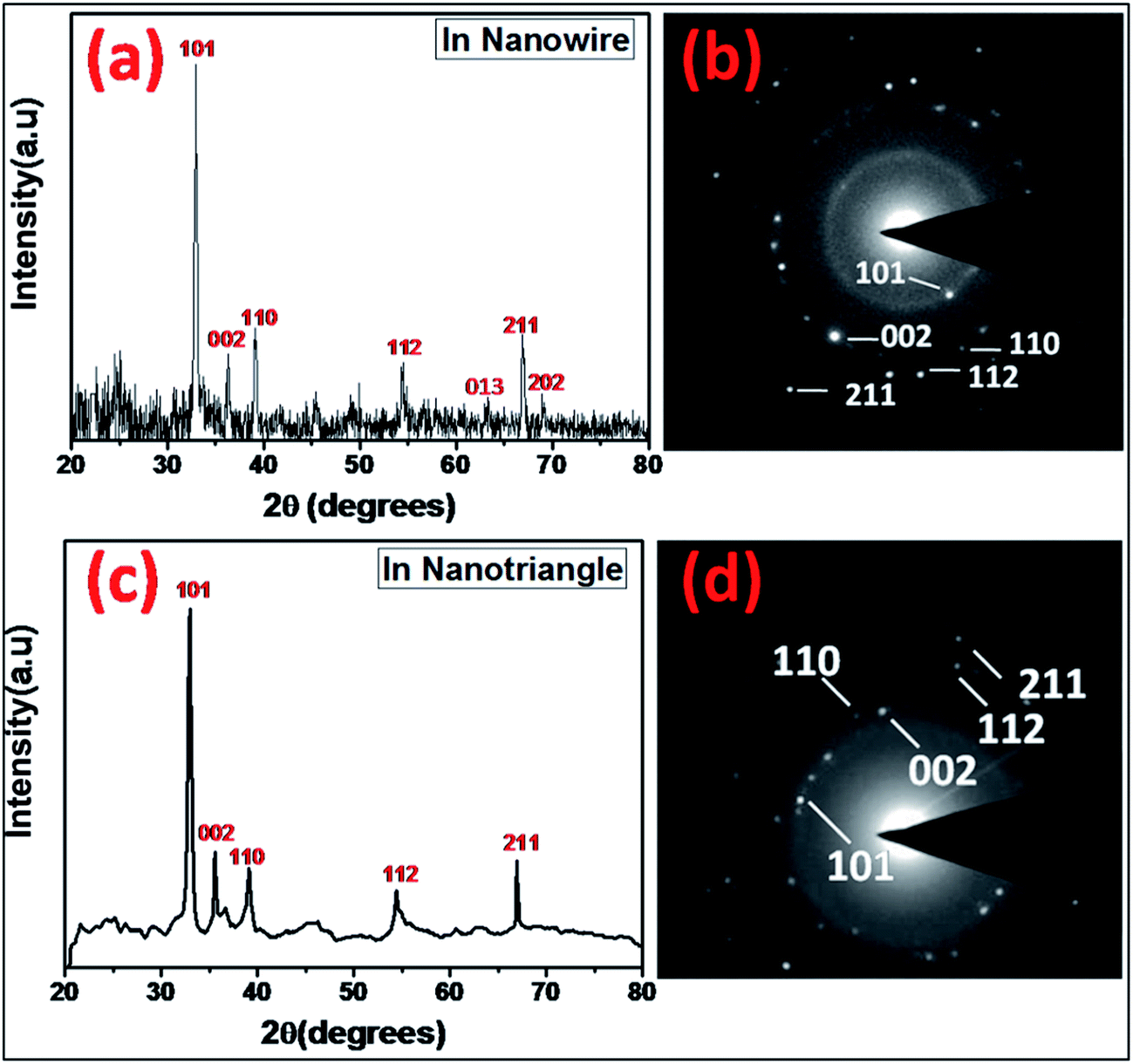 | ||
| Fig. 2 X-ray diffraction and SAED patterns of the In0 (a) and (b) nanowire and (c) and (d) nanotriangle, respectively. | ||
The optical properties of the indium nanoparticles were studied via UV-visible spectroscopy. The In0 nanoparticles exhibit surface plasmon resonance (SPR) over a wide wavelength range from DUV (200 nm) to visible (559 nm) regions.24,43 Fig. 3(a) and (b) presents the absorption spectra of the In0 nanowires and nanotriangles dispersed in ethanol, respectively. The optical density spectrum displays typical absorption maximum near 345 nm for nanowires and 336 nm for nanotriangles, which matches well with the reported SPR band for the In nanostructures.24,35 The identical surface coatings and solvent allows a direct comparison of the optical properties and plasmon resonance of the obtained anisotropic indium nanoparticles. The UV-visible spectra demonstrate an evident size and shape-dependent shift of the SPR wavelength of In0 particles as known for Au and Ag nanoparticles.44 However, 1-D nanostructures, such as nanowires, have been reported to display SPR with distinctive transverse and longitudinal resonance modes.45 The transverse and longitudinal response is sensitive and significantly influenced by the orientation and aspect ratio of the nanowires. TEM images clearly feature In nanowires with varied aspect ratios oriented in different directions resulting in a single and broad UV absorption peak. Moreover, the coupling of plasmon modes due to the presence of nanoparticle clusters or closely spaced nanostructures leads to the observed broadening of the absorption spectrum.46 Further, both absorption spectra display a noticeable optical density in the longer wavelength red region, corresponding to the laser wavelength (633 nm) used for Raman measurements. This broad and extended absorption in the red region typically results either from a small portion of relatively larger nanoparticles or from nanoparticle aggregates, consistent with the TEM results showing the presence of both smaller and larger nanocrystals. The UV-visible spectra clearly depict tunable SPR from indium nanoparticles that can be achieved through size and shape modifications of the anisotropic nanoparticles as in the case of noble metal nanoparticles.
 | ||
| Fig. 3 Absorption spectra of indium (a) nanowires and (b) nanotriangles. | ||
The chemical state of elements in the as-prepared In0 nanoparticles was investigated via XPS analysis. The indium 3d core level spectra of wire- and triangular-shaped nanoparticles resolved into spin–orbit doublets 3d5/2 and 3d3/2 are shown in Fig. 4(a) and (b). In both spectra, the two peaks located at 443.6 eV and 451.2 eV correspond to the characteristic binding energies of metallic indium.47 Moreover, the spectra of both samples appear nearly identical, indicating that both samples comprise indium with identical nature.
 | ||
| Fig. 4 In 3d core level XPS spectra of indium (a) nanowires and (b) nanotriangles. | ||
The SERS activity of the shape-tailored indium nanoparticles was investigated with the prepared substrate for tryptophan as a model analyte. Tryptophan is an important amino acid that forms the molecular basis of proteins and enzymes and efficiently scatters under visible excitation. Thin films of tryptophan (10 μL, 10−7 M) on indium-coated substrates were prepared, as shown in the schematic in Fig. 5(a). In addition, 10 μL of 1 mM tryptophan solution was deposited on a bare cover-slip substrate as a reference. A He–Ne laser with the emission wavelength at 632.8 nm was used as the excitation source. In the Raman measurements, the laser beam with a power of 0.85 mW was focused on the sample using an objective lens (10×, NA = 0.4) to reduce the photoinduced degradation of the molecules and to allow the collection of Raman signal for a reasonably longer integration time (10 s). The scattered light from the sample was then collected in a backscattering configuration.
 | ||
| Fig. 5 (a) Schematic of the SERS substrate preparation; (b) Raman spectra of tryptophan molecules deposited on triangular and wire-shaped indium nanoparticle coated and bare cover-slips; (c) peak intensities of the 1612 cm−1 band of tryptophan at different concentrations with indium nanowire and nanotriangle. | ||
The measured Raman spectra, as shown in Fig. 5(b), of tryptophan films adsorbed on the indium-coated glass substrates clearly show a large enhancement in the SERS signal of the tryptophan molecules. In the spectra, prominent peaks were observed at 1612, 1570, 1361, 1275, 1203, 1159, 1072, 799, and 756 cm−1, ascribed to the vibrational modes of tryptophan.48 The indium-coated substrates display wavenumber shift as well as enhanced spectral intensities of all the bands as compared to the reference substrate. The three weak bands at 1275, 1203, and 1159 cm−1 can be attributed to the δ(CH) vibrations of the indole fragment, and the intense peak at 1361 cm−1 is due to the aliphatic δ(CH2) vibrational modes. The peaks at 1570 and 1612 cm−1 correspond to deformation of the NH3+ species and the ν(COO−) vibration modes of the amino acid fragment. A number of bands below 1000 cm−1 are observed probably due to various δ(CO), ring skeletal, γ(COO−), and ρ(COO−) Raman vibrations. The band assignment clearly suggests that the amino acid fragment interacts with the metal surface through the COO− and NH3+ groups. However, the observed spectral modifications of the Raman bands indicate the degree of interaction and proximity of various functional groups of tryptophan molecule with the metallic substrate. Thus, the measured Raman signal strongly depends on various conformations and orientations of the molecular fragments on the surface.49 In Fig. 5(c), the measured Raman peak intensity of the strongest 1612 cm−1 line for varying concentrations of tryptophan is plotted for indium nanowire and nanotriangle substrates. It can be noticed that nanotriangles provide higher enhancement as compared to nanowires for all the concentrations of tryptophan. For quantitative estimation of the signal enhancement in the SERS, the baseline corrected and well-isolated peak with the maximum intensity at 1612 cm−1 was examined. The SERS enhancement was calculated according to the equation,
 | (1) |
The magnitude of SERS intensity in a complex metal–molecule system depends on several parameters. Thus, the two most influential factors dominating the SERS enhancement mechanism of an analyte are (i) the proximity of the molecule to the metallic surface and (ii) the density of the hotspots.50 The distance dependence of the molecular bands from the active surface thereby yields complex Raman spectra of the target molecule. Real-time experiments preclude contributions of size, shape, orientation, and distribution of the metal nanoparticles on the substrate as well as random distance of the analyte from the metal surface. Moreover, the particle size and morphology, as observed from the TEM images, can expand the LSPR wavelength range, as evident from the absorption spectra. The precise control over particle size and morphology allows tuning of the LSPR peak wavelength and optimization of the SERS enhancement factor. The optical properties of the metal nanostructures are highly sensitive to their shape than to their size, and the complex nanostructures usually have multiple non-degenerated dipole modes, resulting in red-shifted broad plasmon absorption spectra. In addition, for larger particles such as nanotriangles with larger edge-lengths or nanowires with larger diameters, the scattering cross-section increases and the LSPR resonances are red-shifted. Thus, upon excitation at different laser wavelengths, different morphologies would result in different SERS enhancement factors. Reports on Ag and Au nanotriangles clearly demonstrate that the magnitude of SERS enhancement increases with the shape of the asymmetrical nanostructures with an enhancement factor of the order of ∼107.51,52 Upon near resonant excitation closer to the SPR peak wavelength, much higher amplification of the electric field can be obtained, leading to higher magnitude of the SERS enhancement factor as compared to non-resonant excitation. However, formation of nanoparticle assembly or coupling of particles with increased local curvatures such as sharp tips or corners (see ESI, Fig. S3†) generates hot junctions of localized electromagnetic fields that can lead to many-fold increment of SERS enhancement and molecular specificity, referred to as the lightning rod effect.53 Moreover, in the experiments, the SERS enhancement is observed to be independent of the plasmon resonances, matching exactly the excitation or scattering wavelengths. Several reports of optimised processes using metal nanoparticles and nanostructured substrates clearly indicate that the strong SERS effect is not governed singly by the intrinsic SPR response of the material, but is rather dominated by the hot spots, particularly for complex geometries.54 Generally, the extinction spectra of the synthesized nanoparticles dispersed in a solvent display an isolated plasmon peak in response to overall contributions from all the nanostructures. However, the hot spots can be simply generated via the coupling of nanoparticles, which generate strong electrical fields in response to the induced plasmon resonances transmitting on the entire indium-coated substrates. Consequently, the plasmon resonance absorption corresponding to the nanoparticles arranged in film geometries is broad and thus can utilise longer excitation wavelengths for an efficient non-resonant Raman effect.
Simulations based on three-dimensional finite-difference time-domain (FDTD) method were carried out to further comprehend the effect of electromagnetic field intensity distribution on the SERS enhancement and correlate the experimental results. For quantitative understanding, we calculated the EM field generated around both the In nanoparticle geometries with a plane wave at Raman excitation wavelength 633 nm and polarization parallel to the substrate. The electrical field contours for the In nanowire and nanotriangle arranged in monomer and different dimer configurations with water as the background medium are shown in Fig. 6(a) and (b), respectively. The spatial field intensity maps clearly show that the electric field is significantly localized at the vertices or corners of the plasmonic nanostructures, generating amplified EM field in their near regions even for excitation far from the LSPR wavelength. The local electric field confinement and amplification around anisotropic metallic nanostructures is strongly dependent on the shape of the metal particle, both through the effectiveness of shape tunable excitation of the LSPR frequency and the lightening rod effect.55 Albeit the lightening rod effect is a geometrical phenomenon, it can result in larger near-electric field localization for the nanoparticles with the sharpest surface features such as sharp edges or corners.56 The maximum calculated local electric field |E|2 values of ∼52 and ∼90 were respectively achieved for nanowire and nanotriangle monomer particles and are shown as bright spots localized at the top edges. Further, the calculated |E|2 values for the dimer geometries of nanowire and nanotriangle along a fixed polarization axis are shown in Fig. 6(a) and (b), respectively. It is clearly evident from these results that the |E|2 factor multiplies to approximately 3-fold in the case of a nanowire and 5-fold in case of a nanotriangle for a dimer configuration; hence, larger enhancements are expected for bigger ensembles of In NPs. Since in the case of SERS, the intensity enhancement factor (EF) scales with |E|4, the maximum calculated EF could be estimated to be of the order of ∼105 in the case of a nanotriangle and ∼104 in the case of a nanowire, which can elevate further for larger ensembles of particles. Similar SERS enhancement factor is also reported for aluminium nanoparticles with various morphological alterations, such as sharp metallic tips, bow ties, and nanovoids, mostly under UV-DUV excitation.16,18,49 The large EM field enhancements are credited to the ability of metal NP dimers and aggregates to confine incident light around themselves and in the nanoscale gaps between them, resulting into hot junctions, clearly evident from the simulated images of the spatial near-field intensity maps.57 However, this large enhancement of the tip or corner located EM field would be limited to highly localized areas and mostly occur in the gaps between nanoparticle arrays. The majority of the Raman signal is expected to originate from the molecules adsorbed on the top surface of the nanoparticles rather than the very small number of molecules located in these dense hot spots. Since the top surface accounts for a very small area of the nanoparticles, the average enhancement factor experimentally obtained was ∼103 for a nanotriangle and ∼102 for a nanowire. The sharp tips of the triangular nanoparticle contribute significantly towards larger field enhancement as compared to the corners in the nanowires, thereby leading to the observed higher Raman intensity for the In nanotriangle SERS substrate.19 Moreover, the colloidal suspension, comprising nanoparticle mixtures with varying degrees of tip truncation in the case of nanotriangles and rounding of corners for nanowires, further limits the maximum field enhancement around the nanoparticles. In addition, indium nanoparticles form oxide layer upon exposure to air, resulting in rounding of the sharp curvatures, thereby reducing its effectiveness and limiting the enhancement. The experimentally observed lower enhancement factor may be due to difference between the nanoparticle parameters used for simulation and actual parameters of the self-assembled nanoparticles in film geometry. However, the simulation results provide an understanding of the shape-dependent near-field enhancement of indium nanoparticles and observed non-resonant SERS enhancement.
 | ||
| Fig. 6 Electric field contours of indium (a) nanowire and (b) nanotriangle for monomer and dimer geometries with a 5 nm inter-particle gap. | ||
Conclusions
In conclusion, we demonstrated indium as an efficient plasmonic active material for the shape-controlled SERS activity for tryptophan molecules under non-resonant condition. The SERS activity for indium nanotriangle and nanowire nanoparticles, synthesized via a controlled borohydride reduction method, was examined and found to be highly sensitive to the shape of the metal nanostructures. The average enhancement factor obtained from the tryptophan films deposited on the indium-coated substrates was ∼103 for the nanotriangle and ∼102 for the nanowire. The enhancement in the SERS signal can be attributed to the increased EM near-field around the nanoparticles that is strongly influenced by the sharp tips and edges of the indium nanostructures. The highly curved surface features can lead to enormous enhancement of the incident electric field localized at the tips or corners and their interparticle gaps, creating hot spots. The density and localization of these hot spots region rather than the intrinsic LSPR response enhances and dominates the Raman signal from the molecules adsorbed in these junctions, even under non-resonant excitation. These results demonstrate that the anisotropic particles with sharp tips and corners could be the suitable substrate for achieving large SERS enhancement. FDTD simulations clearly display enhancement of the near-field highly localized at the tips or corners and in the interparticle gaps, and the results agree well with the experimentally obtained shape-dependent SERS activity of the indium nanotriangle and nanowire. Further optimization of In nanoparticles with sharp tips or branching morphology and resonant SERS study under UV-DUV excitation can lead to even higher order of enhancements. Thus, facile synthesis combined with highly reproducible SERS enhancements make indium an attractive as well as a promising alternate candidate as an efficient SERS substrate for ultra-low molecular detection.Conflict of Interest
The authors declare no competing financial interest.Acknowledgements
We would like to acknowledge TEM facility, the Kusuma School of Biological Sciences and Project No. RPO 2498 of Indian Institute of Technology (IIT) Delhi for carrying out the TEM investigations. The Department of Physics, IIT Delhi, is acknowledged for XRD and XPS facilities. We would also like to acknowledge FIST (DST Govt of India) UFO scheme of IIT Delhi for Raman measurements.References
- A. Campion and P. Kambhampati, Chem. Soc. Rev., 1998, 27, 241–250 RSC.
- K. Kneipp, Y. Wang, H. Kneipp, L. T. Perelman, I. Itzkan, R. R. Dasari and M. S. Feld, Phys. Rev. Lett., 1997, 78, 1667–1670 CrossRef CAS.
- H. A. Atwater, Sci. Am., 2007, 296, 56–63 CrossRef CAS PubMed.
- M. R. Jones, K. D. Osberg, R. J. Macfarlane, M. R. Langille and C. A. Mirkin, Chem. Rev., 2011, 111, 3736–3827 CrossRef CAS PubMed.
- M. Achermann, J. Phys. Chem. Lett., 2010, 1, 2837–2843 CrossRef CAS.
- K. M. Kosuda, J. M. Bingham, K. L. Wustholz and R. P. Van Duyne, In Comprehensive Nanoscience and Technology, Academic Press: Oxford, U.K., 2011, vol. 3 Search PubMed.
- E. C. Le Ru and P. G. Etchegoin, Annu. Rev. Phys. Chem., 2012, 63, 65–87 CrossRef CAS PubMed.
- S. Boca-Farcau, M. Potara, T. Simon, A. Juhem, P. Baldeck and S. Astilean, Mol. Pharmaceutics, 2014, 11, 391–399 CrossRef CAS PubMed.
- C. Wu, X. Zhou and J. Wei, Nanoscale Res. Lett., 2015, 10, 354–359 CrossRef PubMed.
- C. Wang, B. Liu and X. Dou, Sens. Actuators, B, 2016, 231, 357–364 CrossRef CAS.
- F. Liebig, R. M. Sarhan, C. Prietzel, A. Reineckec and J. Koetz, RSC Adv., 2016, 6, 33561–33568 RSC.
- B. H. Nguyen, V. H. Nguyen and H. N. Tran, Adv. Nat. Sci.: Nanosci. Nanotechnol., 2016, 7, 033001–033012 CrossRef.
- J. M. Sanz, D. Ortiz, R. Alcaraz de la Osa, J. M. Saiz, F. Gonzalez, A. S. Brown, M. Losurdo, H. O. Everitt and F. Moreno, J. Phys. Chem. C, 2013, 117, 19606–19615 CAS.
- T. Dorfer, M. Scmitt and J. Popp, J. Raman Spectrosc., 2007, 38, 1379–1382 CrossRef.
- T. Ding, D. O. Sigle, L. O. Herrmann, D. Wolverson and J. J. Baumberg, ACS Appl. Mater. Interfaces, 2014, 6, 17358–17363 CAS.
- A. Taguchi, N. Hayazawa, K. Furusawa, H. Ishitobi and S. Kawata, J. Raman Spectrosc., 2009, 40, 1324–1330 CrossRef CAS.
- Y. Ekinci, H. H. Solak and C. David, Opt. Lett., 2007, 32, 172–174 CrossRef CAS PubMed.
- D. O. Sigle, E. Perkins, J. J. Baumberg and S. Mahajan, J. Phys. Chem. Lett., 2013, 4, 1449–1452 CrossRef CAS PubMed.
- G. H. Chan, J. Zhao, G. C. Schatz and R. P. Van Duyne, J. Phys. Chem. C, 2008, 112, 13958–13963 CAS.
- L. Cui, S. Mahajan, R. M. Cole, B. Soares, P. N. Bartlett, J. J. Baumberg, I. P. Hayward, B. Ren, A. E. Russell and Z. Q. Tian, Phys. Chem. Chem. Phys., 2009, 11, 1023–1026 RSC.
- F. Magnan, J. Gagnon, F. G. Fontaine and D. Boudreau, Chem. Commun., 2013, 49, 9299–9301 RSC.
- A. I. Dragan and C. D. Geddes, J. Appl. Phys., 2010, 108, 094701–094707 CrossRef.
- J. M. McMahon, G. C. Schatz and S. K. Gray, Phys. Chem. Chem. Phys., 2013, 15, 5415–5423 RSC.
- H. Li, C. Liang, M. Liu, K. Zhong, Y. Tong, P. Liu and G. A. Hope, Nanoscale Res. Lett., 2009, 4, 47–53 CrossRef CAS PubMed.
- C. Kind and C. Feldmann, Chem. Mater., 2013, 23, 4982–4987 CrossRef.
- V. S. Tiwari, T. Oleg, G. K. Darbha, W. Hardy, J. P. Singh and P. C. Ray, Chem. Phys. Lett., 2007, 446, 77–82 CrossRef CAS.
- Z. Li, X. Tao, Y. Cheng, Z. Wu, Z. Zhang and H. Dang, Mater. Sci. Eng., A, 2005, 407, 7–10 CrossRef.
- R. A. Ganeev, A. I. Ryasnyanskiy, U. Chakravarty, P. A. Naik, H. Srivastava, M. K. Tiwari and P. D. Gupta, Appl. Phys. B: Lasers Opt., 2007, 86, 337–341 CrossRef CAS.
- S. Kar, S. Santra and S. Chaudhuri, Cryst. Growth Des., 2008, 8, 344–346 CAS.
- P. K. Khanna, K. W. Jun, K. B. Hong, J. O. Baeg, R. C. Chikate and B. K. Das, Mater. Lett., 2005, 59, 1032–1036 CrossRef CAS.
- U. Jeong, Y. Wang, M. Ibisate and Y. Xia, Adv. Funct. Mater., 2005, 15, 1907–1921 CrossRef CAS.
- Y. Sun and Y. Xia, Adv. Mater., 2002, 14, 833–837 CrossRef CAS.
- S. M. Humphrey, M. E. Grass, S. E. Habas, K. Niesz, G. A. Somorjai and T. D. Tilley, Nano Lett., 2007, 7, 785–790 CrossRef CAS PubMed.
- Y. Kumamoto, A. Taguchi, M. Honda, K. Watanabe, Y. Saito and S. Kawata, ACS Photonics, 2014, 1, 598–603 CrossRef CAS.
- N. H. Chou, X. Ke and R. E. Schaak, J. Am. Chem. Soc., 2008, 130, 8140–8141 CrossRef CAS PubMed.
- E. D. Palik, Handbook of optical constants of solids, Academic Press, New York, 1985 Search PubMed.
- Y. Zhang, M. E. Grass, S. E. Habas, F. Tao, T. Zhang, P. Yang and G. A. Somorjai, J. Phys. Chem. C, 2007, 111, 12243–12253 CAS.
- E. C. Scher, L. Manna and A. P. Alivisatos, Philos. Trans. R. Soc., A, 2003, 361, 241–255 CrossRef CAS PubMed.
- L. Gou and C. J. Murphy, Chem. Mater., 2005, 17, 3668–3672 CrossRef CAS.
- B. Wiley, Y. Sun and Y. Xia, Acc. Chem. Res., 2007, 40, 1067–1076 CrossRef CAS PubMed.
- Z. Wu, S. Yang and W. Wu, Nanoscale, 2016, 8, 1237–1259 RSC.
- P. Singh, S. Kumar, A. Katyal, R. Kalra and R. Chandra, Mater. Lett., 2008, 62, 4164–4166 CrossRef CAS.
- H. Li, C. Liang, M. Liu, K. Zhong, Y. Tong, P. Liu and G. A. Hope, Nanoscale Res. Lett., 2009, 4, 47–53 CrossRef CAS PubMed.
- P. P. Edwards and J. M. Thomas, Angew. Chem., Int. Ed., 2007, 46, 5480–5486 CrossRef CAS PubMed.
- R. Gans, Ann. Phys., 1912, 37, 881 CrossRef CAS ; 1915, 47, 270.
- S. A. Maier, P. G. Kik and H. A. Atwater, Appl. Phys. Lett., 2002, 81, 1714–1716 CrossRef CAS.
- C. D. Wagner, W. M. Riggs, L. E. Davis, J. F. Moulder and G. E. Mullenberg, Handbook of X-Ray Photoeletron Spectroscopy, Perkin-Elmer Corporation, Minnesota, 1978 Search PubMed.
- J. S. Suh and M. Moskovits, J. Am. Chem. Soc., 1986, 108, 4711–4718 CrossRef CAS.
- M. Moskovits, Rev. Mod. Phys., 1985, 57, 783–826 CrossRef CAS.
- F. Tian, F. Bonnier, A. Casey, A. E. Shanahan and H. J. Byrne, Anal. Methods, 2014, 6, 9116–9123 RSC.
- J. Kottmann, O. Martin, D. Smith and S. Schultz, Chem. Phys. Lett., 2001, 341, 1–6 CrossRef CAS.
- F. Tian, F. Bonnier, A. Casey, A. E. Shanahan and H. J. Byrne, Anal. Methods, 2014, 6, 9116–9123 RSC.
- M. D. Doherty, A. Murphy, J. Mc Phillips, R. J. Pollard and P. Dawson, J. Phys. Chem. C, 2010, 114, 19913–19919 CAS.
- S. A. Maier, Plasmonics: Fundamentals and Applications, Springer, New York, 2007, p. 162 Search PubMed.
- E. C. Le Ru and P. G. Etchegoin, Principles of Surface-Enhanced Raman spectroscopy, Elsevier, Amsterdam, 2009 Search PubMed.
- L. P. Mayen, J. Oliva, A. T. Castro and E. De la Rosa, Nanoscale, 2015, 7, 10249–10258 RSC.
- G. H. Chan, J. Zhao, G. C. Schatz and R. P. Van Duyne, J. Phys. Chem. C, 2008, 112, 13958–13963 CAS.
Footnote |
| † Electronic supplementary information (ESI) available: TEM images of the In nanoparticles prepared by controlling the reduction rate, XRD pattern of the irregularly shaped In nanoparticles, and TEM images of different geometric configuration of dimers and higher ensembles of In nanoparticles. See DOI: 10.1039/c7ra03317f |
| This journal is © The Royal Society of Chemistry 2017 |