 Open Access Article
Fabrication of Fe2O3 nanowire arrays based on oxidation-assisted stress-induced atomic-diffusion and their photovoltaic properties for solar water splitting
Yiyuan Xie ,
Yang Ju*,
Yuhki Toku and
Yasuyuki Morita
Department of Mechanical Science and Engineering, Graduate School of Engineering, Nagoya University, Nagoya 464-8603, Japan. E-mail: ju@mech.nagoya-u.ac.jp
First published on 14th June 2017
Abstract
In this research, we propose a new simple method to fabricate high-density Fe2O3 nanowire arrays for solar water splitting, based on oxidation-assisted stress-induced atomic-diffusion. In the presence of water vapor, surface oxidation was promoted during the heating process. The driving force induced by the stress gradient was enhanced due to the expansion of the oxidation layer. Therefore, Fe2O3 nanowire arrays were fabricated at a relative low temperature (350 °C) with a high density (8.66 wire per μm2). Using the nanowire array as the photoanode, a photocurrent density of 0.65 mA cm−2 at 1.23 V vs. RHE was achieved in a three-electrode system.
1. Introduction
Nowadays, most of the energy consumed by human beings comes from fossil fuel. Fossil fuel is not an ideal energy resource for the future due to several disadvantages, such as the limited amount, which cannot satisfy the energy demands in the future; moreover, the combustion of fossil fuel produces CO2, one of the main greenhouse gases. As a sustainable clean energy source, hydrogen is an ideal choice for the future. Photoelectrochemical solar fuel production, especially solar water splitting, has been attracting increasing interest, motivated by the recent advances in nanostructured materials and by concerns over the environmental impact of fossil fuels.1Solar water splitting uses only water and solar energy and a catalyst to produce hydrogen. Some semiconductors have shown great potential for this application, such as BiVO4, TiO2, and Fe2O3 with the theoretical maximum solar to hydrogen (STH) efficiencies of 9.2%, 2.0%, and 15%, respectively.2 Fe2O3 is the most promising of these materials due to the small bandgap and the related visible light absorption, natural abundance, low cost, and stability under deleterious chemical conditions. Recently, several reports on doped nanostructure Fe2O3 used for solar water splitting have been published. For example, in 2006, Cesar et al. fabricated the silicon-doped thin hematite film, with the solar to hydrogen conversion efficiency of 2.1%.3 In 2008, Hu et al. reported a platinum-doped thin hematite film with a photocurrent density of 1.43 mA cm−2, at 0.4 V vs. Ag/AgCl.4 In 1999, a nanocrystalline n-Fe2O3 thin-film was synthesized by Khan et al. with a photocurrent density of 3.7 mA cm−2 at 0.7 V vs. saturated calomel electrode (SCE).5 In 2009, Mohapatra et al. used a sono-electrochemical anodization method to grow Fe2O3 nanotube arrays on an Fe plate with a photocurrent density of 1.41 mA cm−2 at 0.5 V vs. Ag/AgCl.6
On the other hand, Fe2O3 nanowire arrays can be fabricated by stress-induced method, as reported previously.7 Nanowire array structure was considered having two advantages used for solar water splitting. The first is that due to the high surface to volume ratio of nanowire structure, it could provide large electrode/electrolyte interface area to enhance the chemical reaction, thereby improving the water splitting performance eventually. The second is that nanowire array could absorb more light energy than the other structures such as thin film or nanoparticulates because the nanowire array is in a 3D structure which can absorb not only the incident light but also the reflected one. Fe2O3 nanowire arrays can be obtained by heating a high-purity iron substrate under ambient conditions, which is a simple and low-cost method. However, because the density of these nanowire arrays is not high enough, they are unfavorable for solar water splitting. In this work, a new method is proposed to synthesize high-density Fe2O3 nanowire arrays on an iron plate, under low-temperature conditions used for solar water splitting. In the presence of water vapor, surface oxidation was promoted during the heating process, thereby enhancing the driving force induced by stress gradient due to the expansion of the oxidation layer. Consequently, it is possible to fabricate high-density Fe2O3 nanowire arrays at a relatively low temperature (350 °C) compared to that used in the traditional method (500–800 °C).8,9
2. Experimental
2.1 Nanowire fabrication
Commercial iron plate with the purity of 99.95% was used as the substrate for the nanowire fabrication. The thickness of the iron plate is 0.1 mm and the size of each substrate is 10 mm × 10 mm.The iron plate was heated by a ceramic heater in an atmosphere of water vapor. In order to find the best conditions for the nanowire array fabrication, some key parameters are investigated, which include the heating temperature, heating time, water vapor volume, and the duration of heating. Heating temperature was set between 250 and 700 °C, as shown in Table 1. A humidifier was used to provide the water vapor condition, with a gas flow rate ranging from 0.2 L h−1 to 1.25 L h−1, as shown in Table 2. Heating time of the iron plate on the ceramic heater was set to 30, 60, and 90 min, respectively, as shown in Table 3. After the fabrication, all the samples were analyzed by scanning electron microscopy (SEM, JSM-7000FK) and X-ray diffraction (XRD).
| No. | Heating time (min) | Temperature (°C) | Water vapor volume (L h−1) |
|---|---|---|---|
| 1 | 90 | 250 | 0.2 |
| 2 | 350 | ||
| 3 | 450 | ||
| 4 | 500 | ||
| 5 | 600 | ||
| 6 | 700 |
| No. | Heating time (min) | Heating temperature (°C) | Water vapor volume (L h−1) |
|---|---|---|---|
| 7 | 90 | 450 | 0.2 |
| 8 | 1 | ||
| 9 | 1.25 |
| No. | Heating time (min) | Heating temperature (°C) | Water vapor volume (L h−1) |
|---|---|---|---|
| 10 | 30 | 450 | 0.2 |
| 11 | 60 | ||
| 12 | 90 |
2.2 Photocurrent measurements
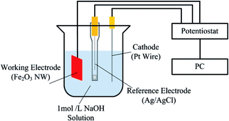
Photocurrent measurement was carried out using a three-electrode system, as shown in Fig. 1. The fabricated Fe2O3 nanowire array is used as the photoanode, the cathode is a Pt wire with a diameter of 0.05 mm, and Ag/AgCl is used as the reference electrode. These three electrodes were placed in a 1 mol L−1 NaOH solution. The light source is a quartz halogen fiber optic illuminator (Fiber-Lite PL800), the spectrum of the light source was measured as shown in Fig. 2, and the optical power density was measured to be 154 mW cm−2 by a power meter (COHERENT LM-10).IPCE measurements were performed using a Xe lamp with the single-wavelength filters from 400 nm to 650 nm. The light energy of the incident light from the lamp was measured with a power meter (COHERENT LM-10). All IPCE measurements were carried out with the applied bias of 0.234 V versus Ag/AgCl reference electrode (1.23 V vs. RHE).
3. Results and discussion
3.1 Experimental results and discussions
Fig. 3 shows the SEM images of the nanowire arrays fabricated at different heating temperatures under the conditions shown in Table 1. It can be inferred from the SEM images that the morphologies of the nanowires are different under different temperatures, besides the density, length, and diameters of the nanowires. The nanowires heated at 350, 450, and 500 °C (Fig. 3(b), (c) and (d), respectively) are cone-shaped and those heated at 600 °C (Fig. 3(e)) and 700 °C (Fig. 3(f)) are wire-shaped. Similar morphologies are observed for a given temperature, indicating that the heating temperature affects the morphology of the nanowire. | ||
| Fig. 3 SEM micrographs of the Fe2O3 nanowire arrays obtained at different heating temperatures: (a) 250; (b) 350; (c) 450; (d) 500; (e) 600; and (f) 700 °C. | ||
The density of the nanowires is a key factor affecting the efficiency of the solar-hydrogen energy cycle. A comparison of the density of the nanowire arrays fabricated at different temperatures is shown in Fig. 4. The largest density of 14.3 wire per μm2 is achieved for the sample heated at 450 °C. When the iron plate was heated at 250 °C, only a small quantity of the nanowires could be observed on the sample surface. With the increase in the heating temperature, the density of the nanowire array increased up to 450 °C. However, it decreased for temperatures above 450 °C. The density is only 1 wire per μm2 at 700 °C.
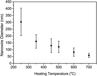
The length and diameter statistics of the nanowires obtained at different temperatures are shown in Fig. 5 and 6, respectively. With the increase in the heating temperature, the average length of the nanowires increased, and the longest nanowires of 9.98 μm average lengths were obtained at 700 °C. Fig. 6 shows the diameter statistic of the nanowires fabricated at different temperatures. Diameters of the nanowires are also considered as an important factor affecting the efficiency of solar to hydrogen energy conversion; nanowires with larger diameters could absorb more light than those with small diameters, which could eventually improve the conversion efficiency. Unlike the variation in the average length, the average diameter of the nanowires decreases with the increase in heating temperature. The largest average diameter of 300 nm was obtained for nanowires fabricated at 250 °C. The effect of the water vapor volume on the nanowire growth was also investigated in this study. The volume of the water vapor was set to be 0.2, 1, and 1.25 L h−1, respectively, as shown in Table 2. From the SEM images shown in Fig. 7, it can be easily observed that the density of the nanowires decreased with an increase in the water vapor volume.
 | ||
| Fig. 7 SEM micrographs of the Fe2O3 nanowire arrays for samples heated at 450 °C with different water vapor volumes: (a) 0.2; (b) 1; and (c) 1.25 L h−1. | ||
Fig. 8 shows the results of the iron samples heated for 30, 60, and 90 min, respectively, under the conditions listed in Table 3. When the sample was heated for a very short duration, some weak spots were generated on the iron plate surface, without any nanowire growth (Fig. 8(a)). In the sample heated for 60 min (Fig. 8(b)), nanowires were formed, but with very different lengths and the density was lower than that of the sample heated for 90 min, as shown in Fig. 8(c). The nanowires had the highest density when the sample was heated for 90 min. The experiments were also carried out with longer heating times, 120 and 150 min, but this did not increase the density of the nanowire array.
 | ||
| Fig. 8 SEM micrographs of the Fe2O3 nanowire arrays fabricated at 450 °C for different heating durations: (a) 30; (b) 60; and (c) 90 min. | ||
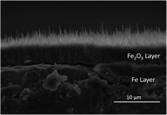
The cross section of the fabricated sample has also observed by using the FESEM, as shown in Fig. 9. Three layers can be easily observed from the SEM image, which include the nanowire layer, the oxide layer and the iron layer. The morphology of the nanowires fabricated at 450 °C was shown in Fig. 10. The shape of nanowires looks like grass, which indicated that nanowires grew from the top of themselves with the precipitation of diffused Fe atoms and their oxidation. The average diameter of the nanowires shown in Fig. 10 is 144 nm, approximately.
3.2 X-ray diffraction and discussions
Fig. 11 shows the XRD patterns of the nanowire arrays obtained for different heating temperatures under the water vapor condition of 0.2 L h−1 and heating time of 90 min. From data obtained from different samples, it can be inferred that when the heating temperature is higher than 450 °C, the formed Fe2O3 layer on Fe substrate is thicker than that formed at 450 °C. By comparing the densities of the nanowire arrays, it is considered that although the heating temperature of over 500 °C could provide a larger driving force to increase the diffusion of the Fe atoms, the formed thicker oxidation layer will hinder the growth of the nanowires, due to the decrease of numbers of weak spots in Fe2O3 layer. Therefore, low density nanowire arrays were obtained at relative high temperatures. In the case of the sample heated at 450 °C, the oxidization rate of the iron plate surface is optimal, generating more weak spots in Fe2O3 layer, and the driving force is also large enough to make the Fe atoms diffuse from the inner part to the Fe/Fe2O3 interface.3.3 Photocurrent measurements
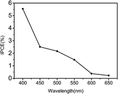
The photovoltaic properties of the nanowires have been investigated using a three-electrode system (Fig. 1), and the results are shown in Fig. 12. The Fe2O3 nanowire photoanode fabricated at 350 °C showed the largest photocurrent density among all the photoanodes, 0.65 mA cm−2 at 1.23 V vs. a reversible hydrogen electrode (RHE). Although the nanowire photoanode fabricated at 450 °C has the largest density of nanowires, the photocurrent density is lower at 0.47 mA cm−2, due to the smaller average diameter of the nanowires (127 nm) compared to that of the nanowire photoanode fabricated at 350 °C (161 nm). The samples heated at 250, 500, 600, and 700 °C show very small photocurrent values, possibly owing to the poor nanowire density.The incident-photon-to-current efficiency (IPCE) of the nanowire photoanode fabricated at 450 °C was measured to confirm the performance of water splitting, as shown in Fig. 13. The IPCE decreased with the increase of wavelength, and the maximum value is 5.54% at 400 nm. This value is relative high than that of other pure Fe2O3 photoanodes without any functional modification, reported by the literatures, such as the Fe2O3 film with the IPCE of 2% at 400 nm,10 and Fe2O3 nanorods with the IPCE of 1.3% at 400 nm.11 It should be mentioned that the IPCE value could be remarkably improved by functional modification of the Fe2O3 nanowire array. It has been reported that the Pt-doped Fe2O3 nanorods can reach the IPCE up to 55% at 400 nm,12 Pt-doped polycrystalline thin-film electrodes of Fe2O3 exhibit an IPCE of 25% at 400 nm,4 and Fe2O3 thin films modified with a catalytic cobalt layer has the IPCE of 46% at 370 nm.13
The stability of photocurrent was measured at 1.23 V vs. RHE by a chopped illumination with 10 s on/off for 120 seconds, for a Fe2O3 nanowire array photoanode fabricated at 450 °C, as shown in Fig. 14. The photocurrent density is very stable and increased and decreased quickly with on and off the light which shows the good photoresponse properties of the Fe2O3 nanowire array photoanode.
 | ||
| Fig. 14 J–t curve of Fe2O3 nanowire array photoanode under chopped illumination at a bias of 0.234 V vs. Ag/AgCl (1.23 V vs. RHE). | ||
3.4 Mechanism
When the iron plates are heated, the thermodynamically stable oxide layer, Fe2O3 topmost layer are formed. Because the molar volumes of Fe2O3 (30.39 cm3 mol−1)14 is great larger than that of Fe (7.09 cm3 mol−1),14 tensile stress is generated in the iron plate due to the volume expansion of Fe2O3 layer.15 Thus, a stress gradient is generated from the center of the Fe plate to the Fe/Fe2O3 interface. The gradient of stress can serve as the driving force for the atomic diffusion and the atomic flux propagates from the low tensile area to high tensile area. Therefore, with the formation of the Fe2O3 layer, the Fe atoms move from the center of Fe plate to Fe/Fe2O3 interface due to the stress-induced atomic diffusion. These diffusion atoms serve as a continuous source for the formation of Fe2O3 nanowires.After the Fe atoms diffuse along the stress gradient to the Fe/Fe2O3 interface, they cumulate at the interface and then find the weak spots of Fe2O3 layer and penetrate them to form nanowires accompanying the oxidation of the Fe atoms. After the nanowires are formed, Fe atoms continue to diffuse along the nanowires due to the high driving force (see Fig. 15), which explains the formation of longer nanowires with the increase in the heating time. Under the water vapor condition, greater amounts of iron can be oxidized into Fe2O3, which could increase the thickness of the Fe2O3 layer on the Fe substrate. Therefore, the tensile stress that the Fe layer suffered from the Fe2O3 layer is much larger in the presence of water vapor than that created under an atmosphere condition. This increase the stress gradient and the driving force for atom diffusion, thereby resulting in an increase in the density of the nanowires. It should be noted that the driving force induced by the stress gradient is due to the volume expansion of the Fe2O3 oxidation layer, which is different from that induced by the thermal expansion mismatch generated in Al/Si16 or Cu/Si17 structured samples. The similar thermal expansion coefficients of Fe2O3 and Fe make it difficult to create a stress based driving force based on thermal expansion mismatch.
4. Conclusions
In summary, a new oxidation-assisted stress-induce method to fabricate high-density semiconductor nanowire array has been demonstrated. Large area Fe2O3 nanowire arrays with high density were fabricated successfully at low temperatures under the water vapor condition. The best growth condition for the Fe2O3 nanowire arrays is heating for 90 min at 350 °C, and a water vapor volume of 0.25 L h−1. Both the density and diameter of the nanowires affect the photocurrent density of the nanowire photoanode, which reached 0.65 mA cm−2 for the nanowire array with the density and diameter of 8.66 wire per μm2 and 161 nm, respectively. The photocurrent measurements indicate the good potential of the Fe2O3 nanowire array photoanodes for solar water splitting.Acknowledgements
This work was supported by the Japan Society for the promotion of science with Grants-in-Aid for Science Research (A) 26249001.References
- F. Le Formal, S. R. Pendlebury, M. Cornuz, S. D. Tilley, M. Gratzel and J. R. Durrant, J. Am. Chem. Soc., 2014, 136, 2564–2574 CrossRef CAS PubMed.
- Z. Chen, H. N. Dinh and E. Miller, Photoelectrochemical Water Splitting: Standards, Experimental Methods, and Protocols, Springer Briefs in Energy, New York, 2013 Search PubMed.
- I. Cesar, A. Kay, J. A. Gonzalez Martinez and M. Grätzel, J. Am. Chem. Soc., 2006, 128, 4582–4583 CrossRef CAS PubMed.
- Y. S. Hu, A. Kleiman-Shwarsctein, A. J. Forman, D. Hazen, J. N. Park and E. W. McFarland, Chem. Mater., 2008, 20, 3803–3805 CrossRef CAS.
- S. U. Khan and J. Akikusa, J. Phys. Chem. B, 1999, 103, 7184–7189 CrossRef CAS.
- S. K. Mohapatra, S. E. John, S. Banerjee and M. Misra, Chem. Mater., 2009, 21, 3048–3055 CrossRef CAS.
- H. Srivastava, P. Tiwari, A. K. Srivastava and R. V. Nandedkar, J. Appl. Phys., 2007, 102, 054303 CrossRef.
- Y. Y. Fu, R. M. Wang, J. Xu, J. Chen, Y. Yan, A. V. Narlikar and H. Zhang, Chem. Phys. Lett., 2003, 379, 373–379 CrossRef CAS.
- X. Wen, S. Wang, Y. Ding, Z. L. Wang and S. Yang, J. Phys. Chem. B, 2005, 109, 215–220 CrossRef CAS PubMed.
- G. Wang, Y. Ling, D. A. Wheeler, K. E. George, K. Horsley, C. Heske, J. Z. Zhang and Y. Li, Nano Lett., 2011, 11, 3503–3509 CrossRef CAS PubMed.
- M. Li, Z. Zhang, F. Lyu, X. He, Z. Liang, M. S. Balogun, X. Lu, P.-P. Fang and Y. Tong, Electrochim. Acta, 2015, 186, 95–100 CrossRef CAS.
- J. Y. Kim, G. Magesh, D. H. Youn, J. W. Jang, J. Kubota, K. Domen and J. S. Lee, Sci. Rep., 2013, 3, 2681 CrossRef PubMed.
- R. S. Schrebler, L. Ballesteros, A. Burgos, E. C. Muñoz, P. Grez, D. Leinen, F. Martín, J. R. Ramos-Barrado and E. A. Dalchiele, J. Electrochem. Soc., 2011, 158, D500–D505 CrossRef CAS.
- Z. Yang, Z. Li, L. Yu, Y. Yang and Z. Xu, J. Mater. Chem. C, 2014, 2, 7583–7588 RSC.
- L. Hu, Y. Ju, A. Hosoi and Y. Tang, Nanoscale Res. Lett., 2013, 8, 445 CrossRef PubMed.
- M. Chen, Y. Yue and Y. Ju, J. Appl. Phys., 2012, 111, 104305 CrossRef.
- Y. Yue, M. Chen, Y. Ju and L. Zhang, Scr. Mater., 2012, 66, 81–84 CrossRef CAS.
| This journal is © The Royal Society of Chemistry 2017 |


