
 Open Access Article
 This Open Access Article is licensed under a
 Creative Commons Attribution 3.0 Unported Licence
Facile synthesis of NiS2@MoS2 core–shell nanospheres for effective enhancement in microwave absorption†
Xiao-Juan Zhang‡
a,
Shan-Wen Wang‡a,
Guang-Sheng Wang *a,
Zhen Li*b,
Ao-Ping Guoa,
Jia-Qiang Zhua,
Da-Peng Liua and
Peng-Gang Yin*a
*a,
Zhen Li*b,
Ao-Ping Guoa,
Jia-Qiang Zhua,
Da-Peng Liua and
Peng-Gang Yin*a
aSchool of Chemistry and Environment, Key Laboratory of Bio-Inspired Smart Interfacial Science and Technology of Ministry of Education, Beihang University, Beijing 100191, P. R. China. E-mail: wanggsh@buaa.edu.cn; pgyin@buaa.edu.cn
bChangjiang River Scientific Research Institute of Changjiang Water Resources Commission, Wuhan, Hubei Province 430010, P. R. China. E-mail: 951419476@qq.com
First published on 24th April 2017
Abstract
Core–shell structured NiS2@MoS2 nanospheres have been successfully fabricated via a facile hydrothermal method. The structure and morphology of the nanospheres were characterized by X-ray diffraction (XRD), X-ray photoelectron spectroscopy (XPS), scanning electron microscopy (SEM), field emission scanning electron microscopy (FESEM) and transmission electron microscopy (TEM). The results indicated that this unique core–shell structure was beneficial to high-performance microwave absorption. A possible absorption mechanism was explained in detail. As an absorber, nanocomposites with a filler loading of 20 wt% exhibited enhanced microwave absorption properties due to characteristic impedance matching, synergistic effects, dipole and interface polarization, multiple reflections and quarter-wavelength matching. The minimum reflection loss can reach −41.05 dB at 12.08 GHz, and the absorption bandwidth exceeding −10 dB is 4.4 GHz with a thickness of 2.2 mm.
Introduction
Nowadays, it is essential to exploit new and highly efficient microwave absorbers against electromagnetic (EM) radiation caused by electronic apparatus or radar systems, which will lead to undesirable EM pollution.1–3 Significant effort has been devoted to designing enhanced microwave absorbers with different morphologies and structures.4–6 Nanomaterials are attracting considerable attention in a variety of fields such as lithium-ion batteries,7 supercapacitors,8–10 energy storage,11 and electrocatalysts for the oxygen reduction reaction and the hydrogen evolution reaction,12,13 as well as EM wave absorbers due to their diverse structural types, abundant and inexpensive nature, especially for metal sulfides. To date, various metal sulfides such as MoS2 nanosheets,14 3D MoS2 nanospheres,15 hierarchical CuS nanospheres,16,17 CdS nanocrystals,18 Bi2S3 nanorods19 and CuS nanoflakes20 have been utilized as EM wave absorbing materials.As is well known, nano-structural engineering is beneficial to improving microwave absorption property. Recently, extensive studies have proved that a variety of nanomaterials with core–shell or yolk–shell structure can be used as high-performance microwave absorbers due to the synergistic effects of both the cores and shells. Compared to single type of wave absorber, multi-components always exhibit much stronger reflection loss. For example, Xu et al.21 investigated the microwave absorption performance of ellipsoidal Fe3O4@CuSiO3 nanorattles with different aspect ratios. Because of the strong magnetic loss and improvement of dielectric loss, they exhibited enhanced microwave absorption property with a minimum reflection loss of −30.8 dB at 8.0 GHz. Liu et al.4 fabricated CoNi@SiO2 core–shell, CoNi@SiO2@TiO2 core–shell–shell and CoNi@Air@TiO2 yolk–shell microspheres in a facile process and investigated their microwave absorption properties, respectively. The results showed that the CoNi@SiO2@TiO2 absorbers exhibited the most enhanced microwave absorption ability. In addition, the research about hierarchical Fe3O4@TiO2 yolk–shell microspheres,22 yolk–shell C@C microspheres,23 FeSn2/Sn/graphite core–shell nanoparticles,24 yolk–shell Fe3O4@ZrO2 structure,25 double-shelled Fe3O4@SnO2 yolk–shell microspheres,26 Fe3O4/C core–shell nanospindles,27 Ni@TiO2 and Ni@SiO2 core–shell microspheres28 et al. has further verified that the core–shell or yolk–shell structure is beneficial to obtaining higher microwave absorption performance.
As for these core–shell or yolk–shell structural wave absorbers, the agglomeration of magnetic core or complicated preparation method restricts their practical application immensely. In order to solve these problems, using metal sulfides is more promising for EM wave absorption property on account of their typical dielectric loss mechanism. Furthermore, reports on core–shell nanostructural wave absorbers composed of transition metal sulfides are still scarce. Based on this, we demonstrate the successful design and fabrication of uniform core–shell NiS2@MoS2 microspheres through a facile hydrothermal route with enhanced microwave absorption performance for the first time. As expected, the synthesized NiS2@MoS2 microspheres exhibits excellent wave absorption property compared with that of single NiS2 or MoS2 nanomaterial.
Results and discussion
As shown in Scheme 1, the NiS2 nanospheres have been fabricated by a simple solvothermal method. After that, the NiS2 nanospheres could play the role of nucleation site for MoS2. The generated MoS2 nanoplates coated on the surface of NiS2 nanospheres due to the strong affinity which caused by homologous inorganic molecules between the nucleation sites and MoS2 nanoplates to form core–shell structural NiS2@MoS2 nanospheres. The wrinkled nanoplates would increase the specific surface area that is beneficial to obtain higher microwave absorption performance.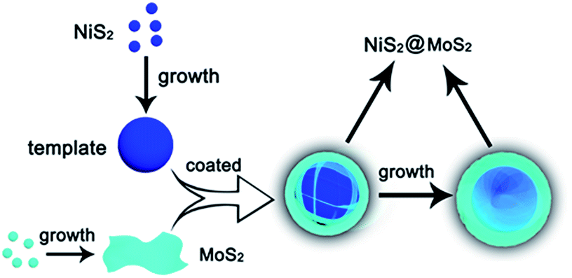 | ||
| Scheme 1 Schematic illustration of the synthetic procedure for the NiS2@MoS2 nanospheres. | ||
In order to study the crystal structure of NiS2 and NiS2@MoS2 nanospheres, the XRD patterns have been provided in Fig. 1a. It can be seen that all the diffraction peaks are readily indexed to the cubic vaesite (JCPDS no. 11-0099). The narrow sharp peaks confirm that the material should be highly crystallized NiS2 without any other impurities. In addition, the XRD pattern of NiS2@MoS2 nanospheres is almost the same as that of NiS2 nanospheres, while the intensity of peaks become weaker due to the coated MoS2 nanoplate. The XRD pattern of MoS2 nanoplate shown in Fig. S1† indicates that the MoS2 nanoplate is weak crystalline and the intensity of peaks is far lower than that of NiS2 nanospheres. As a result, the XRD peaks of MoS2 nanoplate cannot be displayed in the pattern of NiS2@MoS2 nanospheres. To verify the existence of MoS2, the surface chemical states of NiS2@MoS2 nanospheres are further investigated via the X-ray photoelectron spectroscopy (XPS). The core level of the Ni 2p spectrum shown in Fig. 1b can be deconvoluted into two spin–orbit doublets. The peaks at 857.37 and 875.38 eV are attributed to 2p3/2 and 2p1/2 of Ni2+, and the peaks at 861.67 and 880.38 eV are assigned to 2p3/2 and 2p1/2 of Ni3+, respectively. The existence of Ni3+ is mainly due to the slight oxidation of NiS2 on the surface.29 From the Mo 3d spectrum, it certainly turns out that the Mo atom exists as +4 oxidation state. The two peaks at 233.12 eV (Mo4+ 3d3/2) and 229.46 eV (Mo4+ 3d5/2) are from the semiconducting 2H-phase MoS2, and those at 232.22 eV (Mo4+ 3d3/2) and 228.98 eV (Mo4+ 3d5/2) are assigned to metallic 1T-phase MoS2.30 In addition, the nearby S 2s peaks are deconvoluted into two peaks at 226.83 and 225.90 eV, corresponding to the two chemical states of S species bonding with Ni and Mo ions (Fig. 1c). For the S 2p spectra (Fig. 1d), the XPS peak is deconvoluted into four peaks. The peaks at 164.45 and 162.19 eV are assigned to the S 2p1/2 and S 2p3/2 orbitals of divalent sulfide ions (S2−) in MoS2, while the other two peaks at 163.18 and 161.71 eV are attributed to S 2p1/2 and S 2p3/2 of Ni–S bondings. Therefore, the XPS characterization have indicated the successful synthesis of NiS2@MoS2 core–shell nanostructures and suggested a strong interaction between these two phases.31
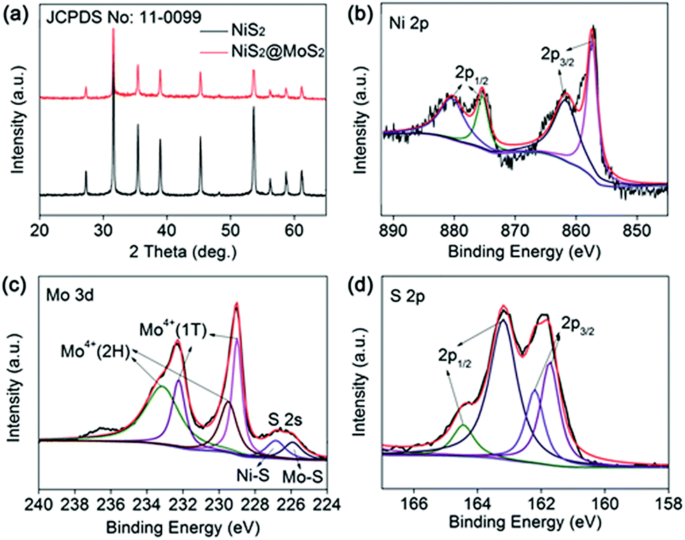 | ||
| Fig. 1 (a) XRD pattern of NiS2 and NiS2@MoS2 nanospheres; XPS spectra of (b) Ni 2p, (c) Mo 3d, (d) S 2p. | ||
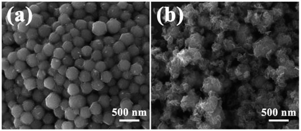
The sizes and morphologies of the as-synthesized NiS2 and NiS2@MoS2 nanospheres were characterized by SEM and TEM. An overview of SEM images (Fig. 2a and b) show the surface morphology, indicating that the particles exhibit uniform nanospheres with smooth or wrinkled surface. A magnified SEM images insetted in Fig. 2a and b reveal that the average diameter of these two samples are about in the range of 200–250 nm and 250–300 nm. To verify the core–shell structure of NiS2@MoS2 nanospheres, the TEM and HRTEM images have been provided in Fig. 2c and d. From the TEM image, it is obviously seen that the solid sphere as core and the curved nanoplates as shell. And the nanoplate-assembled layer is about 25 nm. As shown in Fig. 2d, the ordered lattice fringes are clearly observed from a high-resolution TEM image. The spacings between two neighboring lattice fringes are approximately 0.62 nm and 0.27 nm, corresponding to the (002) and (100) plane of MoS2 shell. Then for NiS2 core, the spacings between two neighboring lattice fringes are approximately 0.33 nm and 0.28 nm, corresponding to the (111) and (200) plane, respectively. Moreover, the FESEM images of NiS2@MoS2 nanospheres presented in Fig. S2† reveal the NiS2 core and MoS2 shell explicitly.
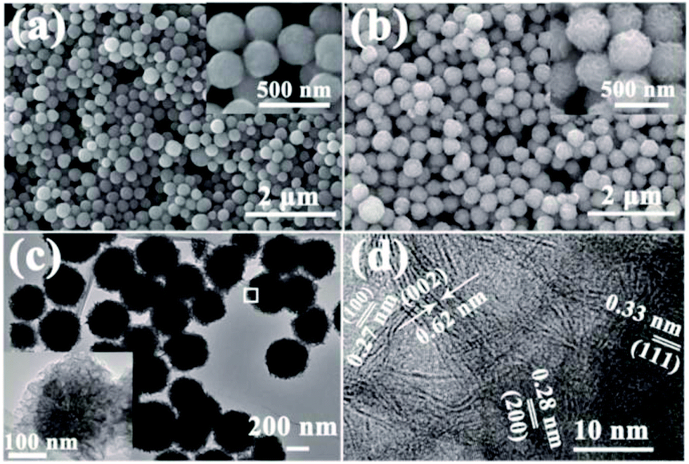 | ||
| Fig. 2 SEM images of (a) NiS2 and (b) NiS2@MoS2 nanospheres. Inset: magnified SEM images; (c) TEM image; (d) high-resolution TEM image of NiS2@MoS2 nanospheres. | ||
To further illuminate the core–shell structure of NiS2@MoS2 nanospheres, the FESEM characterization and the corresponding elemental maps have been displayed in Fig. 3. In the rectangular region, the elemental maps of S, Ni and Mo demonstrate that the NiS2@MoS2 nanospheres are composed of NiS2 core and MoS2 shell indeed. Moreover, as shown in Fig. S3,† the elemental mapping of S, Ni and Mo elements in line-scanning mode and atomic percent correspond to this result. The unique structure is helpful for the high-efficiency electromagnetic-wave absorption property.
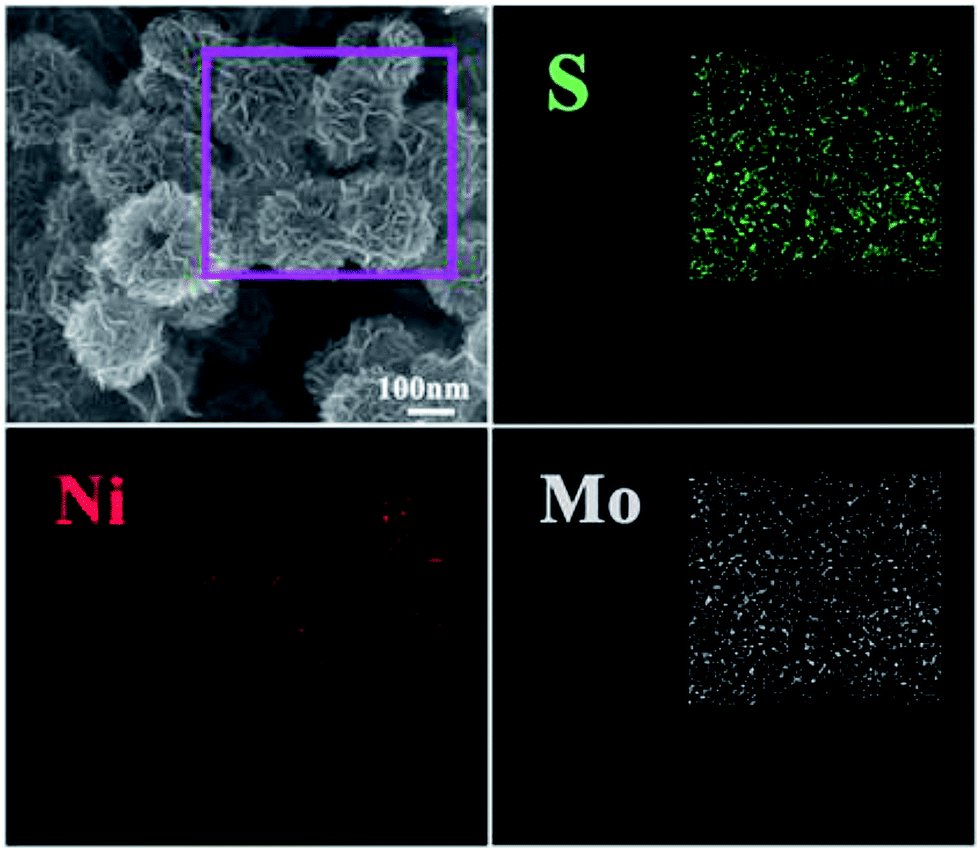 | ||
| Fig. 3 FESEM image of the NiS2@MoS2 nanospheres and corresponding elemental mapping images of S, Ni and Mo. | ||
It is very interesting that the coated state will become very different with variable quantity of sodium molybdate and L-cysteine. As shown in Fig. 4, when the amount of sodium molybdate and L-cysteine decrease to half of the original (0.04 g and 0.08 g), only a little nanoplate coated on the surface of NiS2 nanospheres. On the other hand, when their amounts increase twice compared to the original amount (0.16 g and 0.32 g), much redundant MoS2 nanoplates generate. These results indicate that, with proper control of the relative ratios of sodium molybdate to NiS2 nanospheres, core–shell structural NiS2@MoS2 nanospheres can be successfully fabricated.
 | ||
| Fig. 4 FESEM images of NiS2@MoS2 samples under different conditions: (a) Na2MoO4·2H2O: 0.04 g, L-cysteine: 0.08 g; (b) Na2MoO4·2H2O: 0.16 g, L-cysteine: 0.32 g. | ||
The electromagnetic wave absorption properties of NiS2 and NiS2@MoS2 nanospheres are investigated in terms of reflection loss. According to the transmission line theory, the reflection loss (RL) values are calculated using the measured data of relative permittivity and permeability at a given frequency and thickness layer, which is summarized by the following equations:32
 | (1) |
 | (2) |
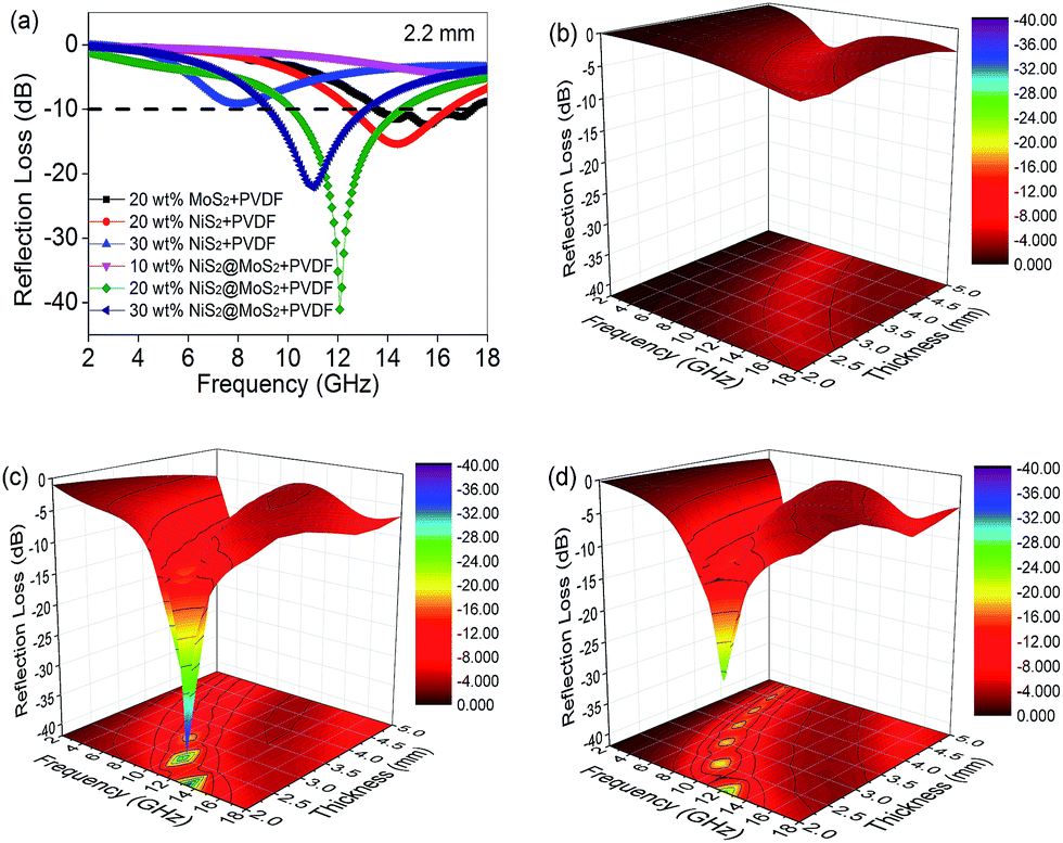 | ||
| Fig. 5 (a) Microwave RL curves of the composites with a thickness of 2.2 mm in the frequency range of 2–18 GHz. Three-dimensional representations of the RL of NiS2@MoS2/PVDF composites with a filler loading of (b) 10 wt%, (c) 20 wt% and (d) 30 wt%. | ||
It is well-known that the electromagnetic wave absorption performance is closely correlated with their complex relative permittivity and permeability, where the real parts of complex permittivity (ε′) and complex permeability (μ′) represent the storage capability of electric and magnetic energy, and imaginary parts (ε′′ and μ′′) stand for the dissipation capability of these two types of energy. Owing to the absence of magnetic components in NiS2 and MoS2, the complex permeability can be ignored. To reveal the microwave absorption mechanism, Fig. 6 shows the complex permittivity of NiS2/PVDF, MoS2/PVDF and NiS2@MoS2/PVDF nanocomposites. It is observed that the core–shell structure has an important impact on the electromagnetic parameters. The NiS2 nanospheres exhibit relatively high complex permittivity without external MoS2 shells. As shown in Fig. 6a and S4,† the ε′ and ε′′ of 30 wt% NiS2/PVDF decreases from 26.5 to 12.6 and from 13.5 to 9.0 with the increase of frequency, which is much higher than that of NiS2@MoS2/PVDF under the same filler loading. The excessive ε′ and ε′′ is not good for characteristic impedance match. As aforementioned, NiS2 and NiS2@MoS2 nanospheres have negligible magnetic loss mechanism, therefore the incident EM wave is attenuated due to single dielectric loss mechanism. The dielectric losses are mainly originated from the electron polarization, the ion polarization and the electric dipole polarization, etc. However, in the microwave range, the electron polarization and the ion polarization are insignificant, while the electric dipole polarization might be a main contributor.24 In theory, the tangent of dielectric loss angle (δε) of the material can be expressed as tan![[thin space (1/6-em)]](https://www.rsc.org/images/entities/char_2009.gif) δε = ε′′/ε′. Fig. 6b displays that the tanδε value of 30 wt% NiS2/PVDF is highest between 0.49 to 0.72 in frequency range of 2–18 GHz. It is unfortunate that the preferable tanδε in NiS2/PVDF fail to endow it with excellent microwave absorption on account of the mismatched characteristic impedance. The 20 wt% NiS2@MoS2/PVDF shows the most enhanced EM wave absorption property while the tanδε value decreases from 0.40 to 0.09 with increasing frequency. This phenomenon indicates that the matched characteristic impedance is not the only influence factor. To illustrate the impact of core–shell structure on microwave absorption performance, we summarized the corresponding performances in Table 1. All these research has proved that the core–shell structure is beneficial for strong wave absorption ability.
δε = ε′′/ε′. Fig. 6b displays that the tanδε value of 30 wt% NiS2/PVDF is highest between 0.49 to 0.72 in frequency range of 2–18 GHz. It is unfortunate that the preferable tanδε in NiS2/PVDF fail to endow it with excellent microwave absorption on account of the mismatched characteristic impedance. The 20 wt% NiS2@MoS2/PVDF shows the most enhanced EM wave absorption property while the tanδε value decreases from 0.40 to 0.09 with increasing frequency. This phenomenon indicates that the matched characteristic impedance is not the only influence factor. To illustrate the impact of core–shell structure on microwave absorption performance, we summarized the corresponding performances in Table 1. All these research has proved that the core–shell structure is beneficial for strong wave absorption ability.
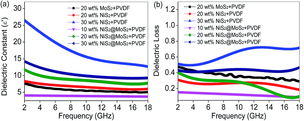 | ||
| Fig. 6 Frequency dependence on (a) real part of the complex permittivity and (b) dielectric loss of samples in the frequency range 2–18 GHz. | ||
| Sample | Minimum RL value (dB) | Thickness (mm) | Filler loading (wt%) | Effective bandwidth (<−10 dB) (GHz) | Ref. |
|---|---|---|---|---|---|
| PPy@PANI | −34.80 | 2.0 | 50.0 | 4.7 | 33 |
| C@C | −34.80 | 2.0 | 50.0 | 5.4 | 23 |
| α-MoO3@PANI | −33.70 | 2.0 | 10.0 | 4.0 | 34 |
| Fe3O4@CuSilicate | −30.80 | 2.0 | 16.7 | 3.5 | 21 |
| Fe3O4@SnO2 | −36.50 | 2.0 | 16.7 | 16.0 | 26 |
| Ni@SiO2 | −40.00 | 1.5 | 70.0 | 3.5 | 28 |
| Ni@TiO2 | −35.40 | 4.0 | 70.0 | 1.0 | 28 |
| Cu@ZnO | −26.70 | 3.0 | — | 1.5 | 35 |
| NiCu alloys | −31.13 | 1.5 | 40.0 | 3.0 | 36 |
| FeSn2@Sn@C | −28.00 | 3.3 | 50.0 | 7.5 | 24 |
| This work | −41.05 | 2.2 | 20.0 | 4.4 | — |
In terms of the quarter-wavelength matching model, the relationship between the predicted matching thickness (tm) and the corresponding matching frequency (fm) can be described by the following equation:37
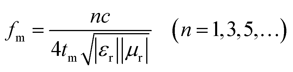 | (3) |
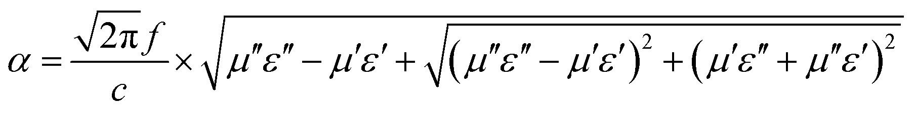
Based on eqn (2), when Zin is close to Z0, the optimal absorption performance of absorber can be achieved. According to previous study,38 when the matching thickness of the samples satisfies eqn (3), Z = |Zin/Z0| is close to 1. Therefore, the minimum RL value can be obtained when the relationship between matching thickness and matching frequency of the absorbers satisfies eqn (3). As mentioned before, the minimum RL value of 20 wt% NiS2@MoS2/PVDF appears at 12.08 GHz under the thickness of 2.2 mm. Using eqn (3), the calculated thickness is 2.15 mm, which is very close to the theoretical thickness of 2.2 mm that is corresponding to wavelength of λ/4. It turns out that the quarter-wavelength matching theory plays an important role. Another key factor that should be considered for an excellent absorber is the attenuation constant α, which determines the attenuation properties of materials, can be determined as:39
 | (4) |
 | ||
| Fig. 7 Attenuation constant of various samples. | ||
Except for the characteristic impedance match and quarter-wavelength matching theory, it is well known that the core–shell structure of NiS2@MoS2 will generate multiple components and more interfaces, leading to a synergistic effect among NiS2, MoS2 and PVDF that is beneficial to improving wave absorption property. In the core–shell structure, surface charges tend to accumulate at the interfaces between two different dielectric media, resulting in dipole polarization. Under an external alternating EM field, the lag of induced charges that counter the increased frequency results in relaxation which is caused by the polarization of defects and transforms EM energy into heat energy.14,40
In addition, after coating with MoS2 shell, the original smooth surface of NiS2 nanospheres turns into wrinkled one, generating larger surface area. Large surface areas can provide more active sites for dissipating and scattering microwaves.41 And according to our previous research about wave absorption performance of 3D MoS2, it is concluded that the laminated structure is able to make the incident microwave generate multiple reflection between the different layers, which will extend the propagation path of electromagnetic wave and greatly enhance their EM wave absorption ability.42 Furthermore, the high-curvature surfaces will lead to more remarkable interface polarization compared with spherical nanoparticles.21
On the basis of the above discussion, the excellent microwave absorption performance of NiS2@MoS2/PVDF is mainly attributed to the unique core–shell structure of NiS2@MoS2 nanospheres which causes characteristic impedance match, synergistic effect among NiS2, MoS2 and PVDF, dipole polarization, interface polarization and multiple reflection. Besides, the quarter-wavelength matching theory is another important wave absorption mechanism. All these mechanism of enhanced microwave absorption have been displayed in Scheme 2 intuitively.
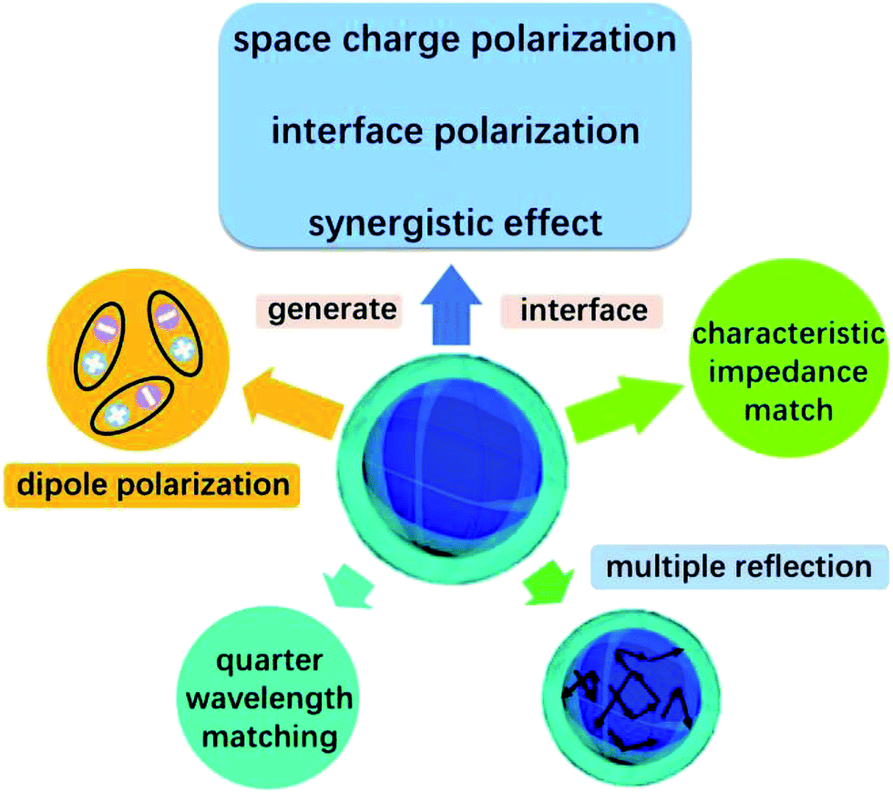 | ||
| Scheme 2 The possible wave absorption mechanism of NiS2@MoS2/PVDF nanocomposites. | ||
Experimental
All chemical reagents were purchased from Lanyi Chemical Company. And all were of analytical grade and used without further purification.Preparation of NiS2 nanospheres
In a typical synthesis, 0.5704 g of nickel chloride hexahydrate (NiCl2·6H2O) and 0.128 g of sulfur powder were dispersed into 60 mL of ethylene glycol (EG) by stirring for 20 min. Then 0.96 g of polyvinyl pyrrolidone (PVP-40000) was added. After stirring for another 30 min, the homogeneous suspension was transferred into Teflon-lined stainless steel autoclave (100 mL). After reacting in 200 °C for 12 h, the solution was cooled to room temperature. The resultant black precipitate of NiS2 nanospheres was washed several times with distilled water and absolute ethanol and finally dried at 60 °C for 12 h for further characterization.
Preparation of core–shell NiS2@MoS2 nanospheres
The core–shell NiS2@MoS2 nanospheres was prepared via a facile hydrothermal method. 0.1 g synthesized NiS2 powder was dispersed into 50 mL of de-ionized water. Then 0.08 g of sodium molybdate (Na2MoO4·2H2O) and 0.16 g of L-cysteine were added. After stirring for 10 min, the homogeneous suspension was transferred into Teflon-lined stainless steel autoclave (100 mL) and reacted in 200 °C for 12 h. The resultant black precipitate of NiS2@MoS2 nanospheres was washed several times with distilled water and absolute ethanol and finally dried at 60 °C for 12 h for further characterization. MoS2 nanoplate has been fabricated by the same method without adding NiS2 powder.Characterization
XRD analyses were carried out on an X-ray diffractometer (D/MAX-1200, Rigaku Denki Co. Ltd., Japan). The XRD patterns with Cu Kα radiation (λ = 1.5406 Å) at 40 kV and 40 mA were recorded in the range of 2θ = 5–80°. Scanning electron microscope (SEM) images were achieved by a FEI Quanta 250 field-emission gun environmental scanning electron microscope at 15 kV with the samples obtained from the thick suspension dropping on the silicon slice. Field emission scanning electron microscopy (FE-SEM) on a JSM-6700F microscope. Transmission electron microscopy (TEM) and high-resolution TEM (HRTEM) investigations were carried out by a JEOL TEM-2100F microscope. X-ray photon spectroscopy was studied with a Thermo Scientific ESCALAB 250 Xi XPS system.EM absorption measurement
The composites used for EM absorption measurement were prepared by mixing the synthesized NiS2 nanospheres and core–shell NiS2@MoS2 nanospheres with polyvinylidene fluoride (PVDF) in different mass percentages, respectively. The mixtures were then pressed into cylindrical-shaped samples (Φout = 7.00 mm and Φin = 3.04 mm). The complex permittivity and permeability values were measured in the 2–18 GHz range with coaxial wire method by an Agilent N5230C PNA-L Network Analyzer.Conclusions
In summary, with NiS2 nanospheres as the cores and nucleation sites, core–shell NiS2@MoS2 nanocomposite have been successfully constructed through a very simple hydrothermal process. It is concluded that the NiS2@MoS2 nanocomposites show substantially enhanced microwave absorption properties as compared to single NiS2 nanospheres or MoS2 nanoplates due to this core–shell structure. With only 20 wt% filler content, the minimum reflection loss of NiS2@MoS2/PVDF composites reaches −41.05 dB at 12.08 GHz with a thickness of 2.2 mm and the absorption bandwidths exceeding −10 dB are 4.4 GHz. Investigations on the mechanism of microwave absorption indicate that their high performance can be caused by characteristic impedance match, synergistic effect and dielectric loss. More importantly, the excellent microwave absorption properties are highly dependent on the quarter-wavelength matching theory. This work will be helpful for the design and development of new novel microwave absorbers with multiple component and unique nanostructure.Acknowledgements
This work was supported by the National Natural Science Foundation of China (51472012) and the Fundamental Research Funds for the Central Universities.Notes and references
- Y. Zhang, Y. Huang, T. Zhang, H. Chang, P. Xiao, H. Chen, Z. Huang and Y. Chen, Adv. Mater., 2015, 27, 2049–2053 CrossRef CAS PubMed.
- Z. J. Li, Z. L. Hou, W. L. Song, X. D. Liu, W. Q. Cao, X. H. Shao and M. S. Cao, Nanoscale, 2016, 8, 10415–10424 RSC.
- X. Zhang, G. Ji, W. Liu, B. Quan, X. Liang, C. Shang, Y. Cheng and Y. Du, Nanoscale, 2015, 7, 12932–12942 RSC.
- Q. Liu, Q. Cao, H. Bi, C. Liang, K. Yuan, W. She, Y. Yang and R. Che, Adv. Mater., 2016, 28, 486–490 CrossRef CAS PubMed.
- B. Zhao, B. Fan, Y. Xu, G. Shao, X. Wang, W. Zhao and R. Zhang, ACS Appl. Mater. Interfaces, 2015, 7, 26217–26225 CAS.
- H. Sun, R. Che, X. You, Y. Jiang, Z. Yang, J. Deng, L. Qiu and H. Peng, Adv. Mater., 2014, 26, 8120–8125 CrossRef CAS PubMed.
- J. Zhou, J. Qin, X. Zhang, C. Shi, E. Liu, J. Li, N. Zhao and C. He, ACS Nano, 2015, 9, 3837–3848 CrossRef CAS PubMed.
- J. Xiao, L. Wan, S. Yang, F. Xiao and S. Wang, Nano Lett., 2014, 14, 831–838 CrossRef CAS PubMed.
- Y. Yan, P. Gu, S. Zheng, M. Zheng, H. Pang and H. Xue, J. Mater. Chem. A, 2016, 4, 19078–19085 CAS.
- H. Pang, X. Li, Q. Zhao, H. Xue, W. Y. Lai, Z. Hu and W. Huang, Nano Energy, 2017, 35, 138–145 CrossRef CAS.
- B. Li, P. Gu, Y. Feng, G. Zhang, K. Huang, H. Xue and H. Pang, Adv. Funct. Mater., 2017, 27, 1605784 CrossRef.
- J. M. Falkowski, N. M. Concannon, B. Yan and Y. Surendranath, J. Am. Chem. Soc., 2015, 137, 7978–7981 CrossRef CAS PubMed.
- J. Yang, D. Voiry, S. J. Ahn, D. Kang, A. Y. Kim, M. Chhowalla and H. S. Shin, Angew. Chem., 2013, 52, 13751–13754 CrossRef CAS PubMed.
- M. Q. Ning, M. M. Lu, J. B. Li, Z. Chen, Y. K. Dou, C. Z. Wang, F. Rehman, M. S. Cao and H. B. Jin, Nanoscale, 2015, 7, 15734–15740 RSC.
- X. J. Zhang, S. Li, S. W. Wang, Z. J. Yin, J. Q. Zhu, A. P. Guo, G. S. Wang, P. G. Yin and L. Guo, J. Phys. Chem. C, 2016, 120, 22019–22027 CAS.
- X. J. Zhang, G. S. Wang, Y. Z. Wei, L. Guo and M. S. Cao, J. Mater. Chem. A, 2013, 1, 12115–12122 CAS.
- S. He, G. S. Wang, C. Lu, J. Liu, B. Wen, H. Liu, L. Guo and M. S. Cao, J. Mater. Chem. A, 2013, 1, 4685–4692 CAS.
- M. Lu, X. Wang, W. Cao, J. Yuan and M. Cao, Nanotechnology, 2016, 27, 065702 CrossRef PubMed.
- X. Luo, G. S. Wang, H. Y. Guo, X. J. Zhang, W. Q. Cao, Y. Z. Wei, L. Guo and M. S. Cao, ChemPlusChem, 2014, 79, 1089–1095 CrossRef CAS.
- P. Liu, Y. Huang, J. Yan, Y. Yang and Y. Zhao, ACS Appl. Mater. Interfaces, 2016, 8, 5536–5546 CAS.
- J. Xu, J. Liu, R. Che, C. Liang, M. Cao, Y. Li and Z. Liu, Nanoscale, 2014, 6, 5782–5790 RSC.
- J. Liu, J. Xu, R. Che, H. Chen, M. Liu and Z. Liu, Chemistry, 2013, 19, 6746–6752 CrossRef CAS PubMed.
- R. Qiang, Y. Du, Y. Wang, N. Wang, C. Tian, J. Ma, P. Xu and X. Han, Carbon, 2016, 98, 599–606 CrossRef CAS.
- X. Zhang, Y. Rao, J. Guo and G. Qin, Carbon, 2016, 96, 972–979 CrossRef CAS.
- M. Yu, C. Liang, M. Liu, X. Liu, K. Yuan, H. Cao and R. Che, J. Mater. Chem. C, 2014, 2, 7275–7283 RSC.
- J. Liu, J. Cheng, R. Che, J. Xu, M. Liu and Z. Liu, J. Phys. Chem. C, 2013, 117, 489–495 CAS.
- X. Liu, X. Cui, Y. Chen, X. J. Zhang, R. Yu, G. S. Wang and H. Ma, Carbon, 2015, 95, 870–878 CrossRef CAS.
- B. Zhao, G. Shao, B. Fan, W. Zhao and R. Zhang, Phys. Chem. Chem. Phys., 2015, 17, 2531–2539 RSC.
- T. An, Y. Wang, J. Tang, W. Wei, X. Cui, A. M. Alenizi, L. Zhang and G. Zheng, J. Mater. Chem. A, 2016, 4, 13439–13443 CAS.
- Z. Yin, X. Zhang, Y. Cai, J. Chen, J. I. Wong, Y. Y. Tay, J. Chai, J. Wu, Z. Zeng, B. Zheng, H. Y. Yang and H. Zhang, Angew. Chem., 2014, 53, 12560–12565 CAS.
- H. Zhu, J. Zhang, R. Yanzhang, M. Du, Q. Wang, G. Gao, J. Wu, G. Wu, M. Zhang, B. Liu, J. Yao and X. Zhang, Adv. Mater., 2015, 27, 4752–4759 CrossRef CAS PubMed.
- Y. Li, J. Zhang, Z. Liu, M. Liu, H. Lin and R. Che, J. Mater. Chem. C, 2014, 2, 5216–5222 RSC.
- C. Tian, Y. Du, P. Xu, R. Qiang, Y. Wang, D. Ding, J. Xue, J. Ma, H. Zhao and X. Han, ACS Appl. Mater. Interfaces, 2015, 7, 20090–20099 CAS.
- Q. Wang, Z. Lei, Y. Chen, Q. Ouyang, P. Gao, L. Qi, C. Zhu and J. Zhang, J. Mater. Chem. A, 2013, 1, 11795–11801 CAS.
- Y. F. Cheng, H. Bi, C. Wang, Q. Cao, W. Jiao and R. Che, RSC Adv., 2016, 6, 41724–41733 RSC.
- B. Zhao, W. Zhao, G. Shao, B. Fan and R. Zhang, ACS Appl. Mater. Interfaces, 2015, 7, 12951–12960 CAS.
- H. Wang, Y. Y. Dai, D. Y. Geng, S. Ma, D. Li, J. An, J. He, W. Liu and Z. D. Zhang, Nanoscale, 2015, 7, 17312–17319 RSC.
- X. Zhang, G. Ji, W. Liu, X. Zhang, Q. Gao, Y. Li and Y. Du, J. Mater. Chem. C, 2016, 4, 1860–1870 RSC.
- X. Hong, Q. Wang, Z. Tang, W. Q. Khan, D. Zhou and T. Feng, J. Phys. Chem. C, 2016, 120, 148–156 CAS.
- T. Wu, Y. Liu, X. Zeng, T. Cui, Y. Zhao, Y. Li and G. Tong, ACS Appl. Mater. Interfaces, 2016, 8, 7370–7380 CAS.
- G. Tong, Y. Liu, T. Cui, Y. Li, Y. Zhao and J. Guan, Appl. Phys. Lett., 2016, 108, 072905 CrossRef.
- M. Chen, L. Zhang, S. Duan, S. Jing, H. Jiang, M. Luo and C. Li, Nanoscale, 2014, 6, 3796–3803 RSC.
Footnotes |
| † Electronic supplementary information (ESI) available. See DOI: 10.1039/c7ra03260a |
| ‡ Xiao-Juan Zhang and Shan-Wen Wang are co-first authors. |
| This journal is © The Royal Society of Chemistry 2017 |