DOI:
10.1039/C7RA03154H
(Paper)
RSC Adv., 2017,
7, 24345-24352
Self-assembled diblock conjugated polyelectrolytes as electron transport layers for organic photovoltaics†
Received
17th March 2017
, Accepted 11th April 2017
First published on 4th May 2017
Abstract
Interfacial morphology is not only paramount for charge extraction and transport but also dramatically affects the morphology of the upper active layer, thereby influencing the ultimate power conversion efficiency. However, detailed investigation of the instinctive self-assembly of conjugated polyelectrolytes (CPEs) as the electron transport layers (ETLs) in polymer solar cells (PSCs) has rarely been investigated. Meanwhile, the correlations between the structural assembly of CPEs ETLs on the crystalline ordering, morphology of the upper active layer and the final photovoltaic performance are mystical stories. Herein, two water/alcohol-soluble diblock CPEs with different backbone PFEO-b-PCNBr and PFEO-b-PTNBr are synthesized via Kumada catalyst transfer coupling reactions as ETLs for inverted bulk-heterojunction PSCs. Both PFEO-b-PCNBr and PFEO-b-PTNBr offer an ohmic contact between the ITO electrode and the active layer by substantially reducing the work function of the ITO via modulating the interfacial dipoles. More intriguingly, the spontaneous self-assembly of the diblock polymers can act as a template to induce the upper active layer to form ordered wide nanowire and nanofiber morphology. The more ordered morphology is beneficial for charge extraction and transportation. Consequently, the devices based on poly(3-hexylthiophene) (P3HT):(6,6)-phenyl-C61 butyric acid methyl ester (PC61BM) with ZnO/PFEO-b-PCNBr and ZnO/PFEO-b-PTNBr as ETLs deliver notable power conversion efficiencies (PCEs) of 3.6% and 3.8%, respectively, which is distinctly enhanced compared to 3.0% for the device with pure ZnO as an ETL. These findings indicate that the self-assembled diblock CPEs ETLs provide a novel strategy for optimization of the morphology of the upper active layer and performance of the PSCs.
Introduction
Bulk heterojunction (BHJ) polymer cells (PSCs) have received increasing attention owing to their advantages, such as mechanical flexibility, low-cost and large-scale roll-to-roll production.1–5 Recently, PSCs have achieved tremendous progress, and the power conversion efficiency (PCE) has been boosted to over 11%.6–9 However, several scientific issues and challenges, such as efficient charge carrier separation, transfer, and collection, must be overcome before large-scale commercial production. To solve these problems, the electrode and the active layer need to form good ohmic interfacial contact and the morphology of the light-harvesting layer can self-assemble into the nanostructure domain.10,11 Good interfacial contact and superior morphologies of the interlayer and active layer are very crucial for efficient charge separation and transportation and collection. If an interfacial layer can simultaneously tune the interfacial barrier and improve the morphology of the active layer, that may be the most promising strategy. Conjugated polyelectrolytes (CPEs) are composed of a delocalized π conjugated backbone and functional polar ionic side chain. Owing to the existence of the polar ionic groups on their side chains, CPEs can realize environmentally friendly water and alcohol processing. In addition, CPEs could avoid intermixing with the upper hydrophobic active layer owing to the orthogonal solubility. Meanwhile, owing to the electrostatic interaction at the interface of CPEs/metal electrode, an aligned interfacial dipole assembly can be formed, which can lower the work function (WF) of the cathode electrode, facilitate the electron extraction and collection, and enhance the PCE of the device.
Diblock conjugated polymers are composed of two different blocks in the backbone, which can self-assemble into ordered nanostructures spontaneously driven by the immiscibility of the blocks and/or crystallinity differences.12,13 If the advantages of diblock conjugated polymers and CPEs are merged, the resulting diblock CPEs (DBCPEs) can possess novel functionalities, such as forming ordered nanostructures, lowering the WF and interfacial barrier, environmentally friendly fabrication, and so on. The obtained self-assembled DBCPEs can not only decrease the interfacial barrier, but also act as a diblock template to induce the upper active layer to form a more ordered nanostructure. However, DBCPEs as the cathode interlayer to modulate the morphology of the upper active layer and diminish the interfacial barrier have rarely been reported. In addition, Maes et al. reported that the nonionic polar oxyalkyl side chains are beneficial for the improvement of the compatibility of the interlayer and the photoactive layer. Meanwhile, the presence of an ionic pendant interlayer leads to the formation of a capacitive double layer, boosting the charge extraction and device efficiency.14 Cationic ammonium ions can endow the polymer with water/alcohol processing and induce the formation of large interfacial dipoles between the active layer and the high work-function metal cathodes.15–21 Based on the above reasons, we designed and synthesized a novel diblock CPE with ethylene oxide and ammonium cationic side chains polar groups, and fluorine and carbazole as blocks, named as poly[(9,9-bis(2′-(2′-(2′-methoxyethoxy)ethoxy)ethyl)-2,7-fluorene)]-block-poly[3-(((6′-N,N,N-trimethylammonium)hexyl)-2,7-carbazole)] (PFEO-b-PCNBr). To explore the detailed relationship between the structural assembly of CPE ETLs on the crystalline ordering, the morphology of the upper active layer and the device photovoltaic performance, the diblock CPE PFEO-b-PTNBr synthesized from our previous literature22 has been used for comparison. Both diblock CPEs PFEO-b-PCNBr and PFEO-b-PTNBr have ethylene oxide and a quaternary ammonium cationic polar side chain; the main difference is the former has fluorine and carbazole diblocks, but the latter has fluorine and thiophene diblocks. In comparison to the bare ZnO ETL, ZnO/PFEO-b-PCNBr and ZnO/PFEO-b-PTNBr ETLs can not only form a more aligned interface dipole to decrease the interfacial energy barrier, but can also act as diblock CPE templates to induce the upper active layer to form well-assembled nanofiber and wide nanowire morphology, which can promote electron extraction and transportation. Consequently, introducing the DBCPEs-modified ZnO as ETLs into the inverted PSCs based on the poly(3-hexylthiophene) (P3HT):(6,6)-phenyl-C61 butyric acid methyl ester (PC61BM) system can dramatically enhance the photovoltaic parameters of the solar cells simultaneously, including the open-circuit voltage (Voc), short-circuit current density Jsc, fill factor (FF) and power conversion efficiency (PCE). The enhancement of the photovoltaic property should be ascribed to the improved morphologies of the interlayer and active layer, as well as the good interfacial contact.
Results and discussion
Synthesis and characterization
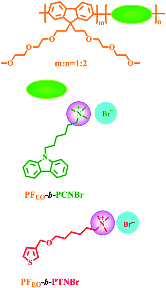
The chemical structures of the diblock polymers FEO-b-PCNBr and PFEO-b-PTNBr are shown in Chart 1 and the detailed synthetic routes of the dibolck polymers are presented in Scheme S1† (the detailed synthetic information is provided in the ESI†). The diblock polymer PFEO-b-PTNBr was synthesized according to our previous literature.22 The diblock polymer PFEO-b-PCBr was first prepared by Kumada catalyst transfer coupling polymerization between 2,7-dibromo-9,9-bis(2-(2-(2-methoxyethoxy)ethoxy)ethyl)-9H-fluorene and 2,7-dibromo-9-(6-bromohexyl)-carbazole. The weight average molecular weight (Mw) and number-average molecular weight (Mn) of PFEO-b-PCBr were estimated by size exclusion chromatograms (SEC) to be 14![[thin space (1/6-em)]](https://www.rsc.org/images/entities/char_2009.gif) 800 and 11800 g mol−1, respectively, with a dispersity index of 1.25. Based on 1H NMR (Fig. S1†), the final obtained ratio between the two blocks polyfluorene and polycarbazole is 1:2. The ionized diblock polymer PFEO-b-PCNBr was obtained through quantitative quaternization of the diblock PFEO-b-PCBr with excess trimethylamine in tetrahydrofuran (THF) solution under −78 °C with liquid nitrogen. The NMR spectrum of PFEO-b-PCNBr is shown in Fig. S2.† Thanks to the polar pendant groups, quaternary ammonium salt and alkoxy group, all the ionized diblock CPEs PFEO-b-PCNBr and PFEO-b-PTNBr can be easily dissolved in polar solvents, such as water, methanol (CH3OH), N,N-dimethylformamide (DMF), and dimethyl sulfoxide (DMSO). In addition, all the intermediates and the final diblock polymers have been thoroughly purified, and the chemical structures of the products are confirmed by nuclear magnetic resonance spectra (NMR).
800 and 11800 g mol−1, respectively, with a dispersity index of 1.25. Based on 1H NMR (Fig. S1†), the final obtained ratio between the two blocks polyfluorene and polycarbazole is 1:2. The ionized diblock polymer PFEO-b-PCNBr was obtained through quantitative quaternization of the diblock PFEO-b-PCBr with excess trimethylamine in tetrahydrofuran (THF) solution under −78 °C with liquid nitrogen. The NMR spectrum of PFEO-b-PCNBr is shown in Fig. S2.† Thanks to the polar pendant groups, quaternary ammonium salt and alkoxy group, all the ionized diblock CPEs PFEO-b-PCNBr and PFEO-b-PTNBr can be easily dissolved in polar solvents, such as water, methanol (CH3OH), N,N-dimethylformamide (DMF), and dimethyl sulfoxide (DMSO). In addition, all the intermediates and the final diblock polymers have been thoroughly purified, and the chemical structures of the products are confirmed by nuclear magnetic resonance spectra (NMR).
 |
| | Chart 1 Structures of the diblock conjugated polyelectrolytes PFEO-b-PCNBr and PFEO-b-PTNBr. | |
Diblock conjugated polymers composed of two different conjugated blocks are well known to self-organize spontaneously at the nanometer scale both in solution and the solid state due to the immiscibility of the blocks and/or crystallinity differences.23,24 Transmission electron microscopy (TEM) was carried out to understand how the introduction of self-assembled templates of diblock CPE ETLs would affect the upper active layer film morphology behavior. Intriguingly, compared with the morphology of pristine ZnO (Fig. 1a), both diblock CPEs modified ZnO show more ordered morphologies as presented in Fig. 1b and c. Obviously, from Fig. 1a for the bare ZnO, we just see the classical ZnO nanoparticles morphology, while for the Fig. 1b, ordered self-assembled dendritic morphology has been observed in ZnO/PFEO-b-PCNBr. ZnO/PFEO-b-PTNBr film is shown in Fig. 1c, and we can find ordered nanofibers morphology. These more ordered morphologies should be ascribed to the self-assembly of the diblock CPE itself and the electrostatic interaction between the diblock CPE and ZnO. More interestingly, in contrast to the morphology of P3HT:PC61BM deposited on bare ZnO (Fig. 1d), insertion of the diblock CPE interlayer between the ZnO and the active layer can realize well optimize the morphology of the upper layer P3HT:PC61BM. As depicted in Fig. 1, on account of the more ordered ZnO/PFEO-b-PCNBr and ZnO/PFEO-b-PTNBr, ETLs can serve as a structural template to induce the upper active layer to form regular molecular orientation, a large amount of ordered wide nanowires and narrow nanofibers are clearly observed in the morphology of P3HT:PC61BM blend films deposited on ZnO/PFEO-b-PCNBr and ZnO/PFEO-b-PTNBr ETLs, respectively (Fig. 1e and f), while no linear structure has been observed for the ZnO/P3HT:PC61BM film. The nanofiber morphologies of the active layers are very favorable for charge separation.
 |
| | Fig. 1 TEM images of (a) bare ZnO, (b) ZnO/PFEO-b-PCNBr, (c) ZnO/PFEO-b-PTNBr, (d) ZnO/P3HT:PC61BM, (e) PFEO-b-PCNBr/P3HT:PC61BM and (f) PFEO-b-PTNBr/P3HT:PC61BM films. | |
In order to further investigate the self-assembly behaviors of ZnO/PFEO-b-PCNBr and ZnO/PFEO-b-PTNBr ETLs on the morphology and crystallization of the upper active layer, the UV-Vis absorption spectra and X-ray diffraction (XRD) patterns of the P3HT:PC61BM active layer with and without CPE substrate are characterized. As shown in Fig. 2a, the UV spectra of P3HT:PC61BM films deposited on ZnO/CPEs show red-shift bands with higher intensity than that of the pristine P3HT:PC61BM film. Moreover, a shoulder peak at 604 nm is detected, indicative of characteristic peaks of the crystalline P3HT.25 In addition, the UV spectrum of P3HT:PC61BM films spin-coated on ZnO/PFEO-b-PTNBr shows a red-shift band compared to that of ZnO/PFEO-b-PCNBr, which may be because the structural difference between fluorene and thiophene is bigger than that of fluorene and carbazole. Diblock polymers are well known to self-assemble into well-ordered nanoscale morphologies spontaneously, which is driven by the thermodynamic incompatibility of the two blocks.26,27 X-ray diffraction (XRD) experiments were employed with the aim of further verifying the superior morphology of P3HT:PC61BM films spin-coated on ZnO/CPEs compared to that of bare ZnO. As described in Fig. 2b, relative to the pristine ZnO/P3HT:PC61BM film, the ZnO/CPEs/P3HT:PC61BM films show stronger (100) reflection peaks at low angle (2θ = 5.47°), corresponding to the lamellar structure of P3HT. Likewise, the P3HT:PC61BM film deposited on ZnO/PFEO-b-PTNBr is sharper compared to that on ZnO/PFEO-b-PCNBr, suggesting that the PFEO-b-PTNBr endows P3HT with better crystallization property. Meanwhile, reflection peaks at angle 2θ = 21.4° associated with the (010) reflection peaks of P3HT have been detected. In addition, the reflection peaks at 2θ = 30.22° and 35.38° are assigned to the (100) and (002) reflection peaks of ZnO, respectively. The XRD results are well consistent with the UV.
 |
| | Fig. 2 (a) Normalized UV-visible absorption spectra and (b) XRD spectra of the bare ZnO/P3HT:PC61BM, ZnO/PFEO-b-PCNBr/P3HT:PC61BM and ZnO/PFEO-b-PTNBr/P3HT:PC61BM. | |
To further clarify the interface interaction and cooperation assembly between the ZnO and CPEs, the X-ray photoelectron spectra (XPS) of pristine ZnO and ZnO/CPEs were obtained and are presented in Fig. 3a. As shown in Fig. 3b, the characteristic N 1s peak (at ∼400 eV) assigned to nitrogen atom in the ZnO/PFEO-b-PCNBr and ZnO/PFEO-b-PTNBr spectra is clearly detected, suggesting that the CPEs are successfully spin-coated on the surface of the ZnO. For bare ZnO, N 1s peaks cannot be observed. The O 1s peak spectra of the bare ZnO and ZnO/CPEs are shown in Fig. 3c. In contrast to the peak in pristine ZnO detected at 530.16 eV, the O 1s peaks for ZnO/PFEO-b-PCNBr and ZnO/PFEO-b-PTNBr are shifted to 529.91 and 529.87 eV, which are shifted towards lower binding energy by 0.25 and 0.29 eV, respectively. The shifts to the lower binding energy may be owing to the higher negative charge density on O2− ions, which originates from the strong interfacial interaction.28,29 Similarly, as shown in Fig. 3d, compared to pristine ZnO 1021.7 eV, the Zn 2p3/2 XPS spectra of ZnO/PFEO-b-PCNBr (1021.4 eV) and ZnO/PFEO-b-PTNBr (1021.3 eV) are shifted to lower binding energy by 0.3 eV and 0.4 eV, implying a strong electrostatic interaction between ZnO and CPEs.
 |
| | Fig. 3 (a) Survey X-ray photoelectron spectra and high-resolution XPS of (b) N 1s, (c) O 1s, and (d) Zn 2p on the surface of ZnO, ZnO/PFEO-b-PCNBr, and ZnO/PFEO-b-PTNBr ETLs on the ITO substrate. | |
To explore surface property and further characterize the interfacial interaction of the ZnO/CPEs bilayers, the water contact angle measurements are carried out (Fig. 4). The water of contact angles for ZnO, ZnO/PFEO-b-PCNBr and ZnO/PFEO-b-PTNBr are 66°, 56° and 52° (Fig. 4a–c), respectively. Interestingly, after annealing, the water contact angles of ZnO/PFEO-b-PCNBr and ZnO/PFEO-b-PTNBr are increased to 67° and 69° (Fig. 4e and f), which reveals that the hydrophobicity of the ZnO/CPEs bilayers been remarkably enhanced upon thermal annealing. As schematically illustrated in Fig. 4d, the enhanced water contact angles could be attributed to some hydrophilic polar side chains of CPEs pointing to the ZnO substrate and hydrophobic diblock conjugated polymer backbone pointing away from ZnO after thermal annealing. The substantially improved hydrophobicity of the ZnO/CPEs could form superior interfacial contact with the upper photon-harvesting layer compared to that of ZnO, in favor of the charge transport and collection.
 |
| | Fig. 4 Water contact angle images of the compounds before (a, b, c) and after (e, f) annealing, (a) bare ZnO, (b, e) ZnO/PFEO-b-PCNBr, (d) the schematic illustration of the side chain orientation of the diblock CPEs ETLs before and after annealing at 150 °C for 10 min, and (c, f) ZnO/PFEO-b-PTNBr. | |
To explore the effect of diblock CPEs on the ZnO ETL, ultraviolet photoelectron spectroscopy (UPS) was used to study the energy levels of the ZnO and ZnO/CPEs ETLs. As presented in Fig. 5a, the high binding-energy cutoffs (Ecutoff) of ZnO, ZnO/PFEO-b-PCNBr and ZnO/PFEO-b-PTNBr are 14.46, 15.11, and 15.18 eV, respectively. The corresponding binding energy onset Eonset is 1.07 eV for bare ZnO, 1.21 eV for ZnO/PFEO-b-PCNBr and 1.05 eV for ZnO/PFEO-b-PTNBr. The highest occupied molecular orbital (HOMO) energies are calculated from the following equation:30
| −HOMO = hν − (Ecutoff − Eonset) |
where
hν is the incident photon energy (
hν = 21.22 eV) for He I. According to the equation, the calculated HOMO energies are −7.83 eV for bare ZnO, −7.32 eV for ZnO/
PFEO-b-PCNBr and −7.09 eV for ZnO/
PFEO-b-PTNBr. The optical gaps of ZnO, ZnO/
PFEO-b-PCNBr and ZnO/
PFEO-b-PTNBr are obtained from the UV-vis absorption spectra to be 3.28 eV, as shown in Fig. S3.
† Based on the values of optical gaps and HOMO, the lowest unoccupied molecular orbital (LUMO) energy levels are −4.55 eV for bare ZnO, −4.04 eV for ZnO/
PFEO-b-PCNBr and −3.81 eV for ZnO/
PFEO-b-PTNBr. The corresponding energy level data are summarized in Table S1.
† The energy-level diagram of the PSCs and electrical contacts of the diblock ZnO/CPEs ETLs based on P3HT:PC
61BM device is presented in
Fig. 5b. The shifts of energy levels among ZnO and ZnO/CPEs demonstrate that diblock CPEs
PFEO-b-PCNBr and
PFEO-b-PTNBr can easily modulate the LUMO level of ZnO. Moreover, after introducing a thin layer of diblock CPEs between ZnO and the active layer, the ETL–active layer interface can form favorable ohmic contact, which is beneficial to charge separation, transfer and collection. The tuning energy levels of ZnO modified by diblock CPEs ETLs indicate that favorable interfacial dipoles are generated between the ZnO and CPEs interface. Although the structures of
PFEO-b-PCNBr and
PFEO-b-PTNBr mainly differ in the backbone, the binding-energy of ZnO/
PFEO-b-PTNBr shifts to the lower energy level in comparison to ZnO/
PFEO-b-PCNBr, indicating that ZnO/
PFEO-b-PTNBr can provide a stronger interfacial interaction and a larger interfacial dipole moment than ZnO/
PFEO-b-PCNBr does. The results are in accordance with those of XPS. To further discuss the interfacial interaction between diblock CPEs and ZnO, Kelvin probe microscopy (KPM) was used to characterize the effective work function (WF) of pristine ZnO and ZnO/CPEs. As depicted in
Fig. 5c, the WF of bare ZnO is 4.41 eV. However, the WF decreased after being modified by diblock CPEs, with a value of 4.33 eV for ZnO/
PFEO-b-PCNBr and 4.20 eV for ZnO/
PFEO-b-PTNBr. In contrast to ZnO/
PFEO-b-PCNBr, ZnO/
PFEO-b-PTNBr possesses a lower WF, which is well consistent with the UPS measurement. In order to more visually understand the variation of WF between ZnO and ZnO/CPEs, the effective work function bar graphs from KPM of the bare ZnO, ZnO/
PFEO-b-PCNBr and ZnO/
PFEO-b-PTNBr ETLs are shown in
Fig. 5d.
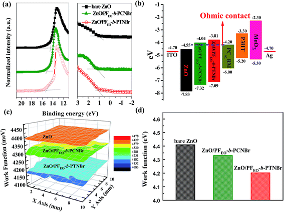 |
| | Fig. 5 (a) Ultraviolet photoelectron spectroscopy (UPS) spectra of the inelastic cutoff region (left) and the HOMO region (right) of ZnO, ZnO/PFEO-b-PCNBr and ZnO/PFEO-b-PTNBr. (b) Energy-level diagram of the PSCs and electrical contacts of the diblock CPEs ETLs based on P3HT:PC61BM device. (c) Work function images from matrix by Kelvin probe microscopy (KPM). (d) Effective work function bar graph from KPM of the bare ZnO, ZnO/PFEO-b-PCNBr and ZnO/PFEO-b-PTNBr ETLs. | |
To explore whether the insertion of diblock CPEs will affect the light absorption of the active layer, the optical transmittance spectra of ZnO and ZnO/CPEs ETLs are investigated as displayed in Fig. S4.† Visibly, the optical transmittance spectra of ZnO and ZnO/CPEs ETLs are almost the same, suggesting that the diblock CPEs layers would not hinder the light-absorption of active layer. To gain insight into the influence of the ZnO/CPEs as ETLs on the photovoltaic performance of the organic solar cells, inverted devices based on ZnO/CPEs ETLs were fabricated with the structure of ITO/ZnO/CPEs/P3HT:PC61BM/MoO3/Ag. The illuminated current density–voltage (J–V) curves of the inverted PSCs based on P3HT:PC61BM active layer with ZnO and ZnO/CPEs ETLs are shown in Fig. 6a, and the corresponding device data are summarized in Table 1. The error bars of Voc, PCE, FF and Jsc are shown in Fig. 6c and d. The device with bare ZnO ETL presents an average PCE of 3.0%, with an open-circuit voltage (Voc) of 0.598 V, short-circuit current density Jsc of 8.216 mA cm−2, and a fill factor (FF) of 61.4%. Delightfully, the PCEs of the devices with ZnO/CPEs ETLs are dramatically enhanced, with PCE of 3.6% and 3.8% for ZnO/PFEO-b-PCNBr and ZnO/PFEO-b-PTNBr, respectively. The improved device efficiencies by introduction of diblock CPEs as modified layers originate from the simultaneous enhancement of device parameters, including Voc, Jsc, FF and PCE. Compared to the Voc of bare ZnO 0.598 V, the Voc has been increased to 0.610 V for ZnO/PFEO-b-PCNBr and 0.616 V for ZnO/PFEO-b-PTNBr. Meanwhile, the FF has been enhanced from 61.4% to 65.4% and 66.1% for ZnO/PFEO-b-PCNBr and ZnO/PFEO-b-PTNBr, respectively. Compared to ZnO/PFEO-b-PCNBr, ZnO/PFEO-b-PTNBr exhibits preferable photovoltaic performance, which should be ascribed to the better morphology of the active layer and the larger interfacial dipole moment. The interfacial ohmic contact created by the diblock CPEs should be responsible for the enhancement of Voc and Jsc. In addition, the improved FF should be ascribed to the more ordered morphologies of the interfacial layer and the active layer. The dark J–V curves are presented in the inset of Fig. 6a. Obviously, the dark current densities of the ZnO/PFEO-b-PCNBr and ZnO/PFEO-b-PTNBr interfacial layers under the reverse bias are smaller in comparison to that of bare ZnO, suggesting that the leakage current at negative voltages has been greatly suppressed by the insertion of diblock CPEs. The dark J–V could also demonstrate that the favorable interfacial dipole moment and interfacial contact caused by diblock CPEs can reduce the leakage current and improve the charge injection efficiency. To further prove the accuracy of Jsc obtained from J–V, the external quantum efficiencies (EQE) are investigated, as presented in Fig. 6b. Quite notably, the devices with ZnO/PFEO-b-PCNBr and ZnO/PFEO-b-PTNBr ETLs exhibit superior EQE values compared to that of ZnO. Moreover, the device based on ZnO/PFEO-b-PTNBr bilayer ETL shows the highest EQE. The EQE results are quite consistent with values acquired from the J–V curves.
 |
| | Fig. 6 (a) J–V curves of devices based on P3HT:PC61BM with various ETLs under the illumination of AM1.5G, 100 mW cm−2 (inset: under dark conditions), (b) EQE characteristics, (c) the error bars of Voc and PCE and (d) the error bars of and FF and Jsc. | |
Table 1 Device performance of inverted P3HT:PC61BM polymer solar cells with various ETLsa
| Cathode buffer layer |
Voc (V) |
Jsc (mA cm−2) |
FF (%) |
PCE (%) |
| The device parameters of each device are obtained from 10 devices, and the ± refers to the standard deviation. |
| ZnO |
0.598 ± 0.004 |
8.216 ± 0.117 |
61.4 ± 0.66 |
3.0 ± 0.054 |
| ZnO/PFEO-b-PCNBr |
0.610 ± 0.002 |
8.990 ± 0.098 |
65.4 ± 0.79 |
3.6 ± 0.055 |
| ZnO/PFEO-b-PTNBr |
0.616 ± 0.006 |
9.260 ± 0.258 |
66.1 ± 1.16 |
3.8 ± 0.044 |
Conclusions
To summarize, a novel self-assembly water/alcohol soluble diblock CPE PFEO-b-PCNBr has been synthesized for the first time and applied as ZnO/PFEO-b-PCNBr bilayer ETL for inverted bulk-heterojunction PSCs based on P3HT:PC61BM. Meanwhile, in order to explore the correlations between the structural assembly of CPEs ETLs on the crystalline ordering, morphology of the upper active layer and device photovoltaic performance, the diblock CPE PFEO-b-PTNBr synthesized from our previous literature was used for comparison. Although the structures of PFEO-b-PCNBr and PFEO-b-PTNBr mainly differ in the backbone, polymer PFEO-b-PTNBr exhibited better performance. Compared with bare ZnO ETL, ZnO/PFEO-b-PCNBr and ZnO/PFEO-b-PTNBr ETLs not only can form a more aligned dipole moment to lower the interfacial energy barrier, but can also act as diblock CPEs templates to induce the upper active layer to form more ordered nanofiber and wide nanowire morphology, which can facilitate the electron extraction and transportation. It should be mentioned that incorporation of the ZnO/CPEs as the bilayer cathode buffer layer can simultaneously enhance the device performance, including Voc, Jsc, FF and PCE. Meanwhile, the superior photovoltaic performance of ZnO/PFEO-b-PTNBr compared to the analogue ZnO/PFEO-b-PCNBr originates from the stronger interfacial dipole moment and better morphology of the active layer, which are beneficial for more efficient charge separation and transfer. Diblock CPEs PFEO-b-PCNBr and PFEO-b-PTNBr have combined the advantages of block polymers and conjugated polyelectrolytes, which can simultaneously tune the interfacial work function and the upper active layer morphology. By proper design and synthesis, diblock CPEs are prospected to be promising candidates to apply in roll-to-roll manufacturing techniques for high performance PSCs.
Conflict of interest
The authors declare no competing financial interests.
Acknowledgements
This work was financially supported by the National Natural Science Foundation of China (51473075), National Basic Research Program of China (973 Program 2014CB260409), Natural Science Foundation of Jiangxi Province (20143ACB20001) and National Science Fund for Distinguished Young Scholars (51425304).
References
- B. C. Thompson and J. M. Frechet, Polymer-fullerene composite solar cells, Angew. Chem., Int. Ed., 2008, 47, 58–77 CrossRef CAS PubMed.
- Y.-J. Cheng, S.-H. Yang and C.-S. Hsu, Synthesis of conjugated polymers for organic solar cell applications, Chem. Rev., 2009, 109, 5868–5923 CrossRef CAS PubMed.
- P. M. Beaujuge and J. M. Frechet, Molecular design and ordering effects in π-functional materials for transistor and solar cell applications, J. Am. Chem. Soc., 2011, 133, 20009–20029 CrossRef CAS PubMed.
- Y. Liu, J. Zhao, Z. Li, C. Mu, W. Ma, H. Hu, H. Lin, H. Ade and H. Yan, Aggregation and morphology control enables multiple cases of high-efficiency polymer solar cells, Nat. Commun., 2014, 5, 5293 CrossRef CAS PubMed.
- W.-Y. Wong and C.-L. Ho, Organometallic photovoltaics: a new and versatile approach for harvesting solar energy using conjugated polymetallaynes, Acc. Chem. Res., 2010, 43, 1246–1256 CrossRef CAS PubMed.
- W. Zhao, D. Qian, S. Zhang, S. Li, O. Inganäs, F. Gao and J. Hou, Fullerene-Free Polymer Solar Cells with over 11% Efficiency and Excellent Thermal Stability, Adv. Mater., 2016, 28, 4734–4739 CrossRef CAS PubMed.
- S. Li, L. Ye, W. Zhao, S. Zhang, S. Mukherjee, H. Ade and J. Hou, Energy-Level Modulation of Small-Molecule Electron Acceptors to Achieve over 12% Efficiency in Polymer Solar Cells, Adv. Mater., 2016, 28, 9423–9429 CrossRef CAS PubMed.
- D. Liu, B. Yang, B. Jang, B. Xu, S. Zhang, C. He, H. Y. Woo and J. Hou, Molecular design of a wide-band-gap conjugated polymer for efficient fullerene-free polymer solar cells, Energy Environ. Sci., 2017, 10, 546–551 CAS.
- J. Zhao, Y. Li, G. Yang, K. Jiang, H. Lin, H. Ade, W. Ma and H. Yan, Efficient organic solar cells processed from hydrocarbon solvents, Nat. Energy, 2016, 1, 15027 CrossRef CAS.
- G. Yu, J. Gao, J. C. Hummelen, F. Wudl and A. J. Heeger, Polymer photovoltiac cells: Enhanced efficiencies via a network of internal donor-acceptor heterojunctions, Science, 1995, 270, 1789 CAS.
- P. E. Shaw, A. Ruseckas and I. D. W. Samuel, Exciton diffusion measurements in poly(3-hexylthiophene), Adv. Mater., 2008, 20, 3516–3520 CrossRef CAS.
- A. Gutacker, S. Adamczyk, A. Helfer, L. E. Garner, R. C. Evans, S. M. Fonseca, M. Knaapila, G. C. Bazan, H. D. Burrows and U. Scherf, All-conjugated polyelectrolyte block copolymers, J. Mater. Chem., 2010, 20, 1423–1430 RSC.
- M. He, F. Qiu and Z. Lin, Conjugated rod–coil and rod–rod block copolymers for photovoltaic applications, J. Mater. Chem., 2011, 21, 17039–17048 RSC.
- J. Kesters, S. Govaerts, G. Pirotte, J. Drijkoningen, M. Chevrier, N. Van den Brande, X. J. Liu, M. Fahlman, B. Van Mele, L. Lutsen, D. Vanderzande, J. Manca, S. Clément, E. Von Hauff and W. Maes, High-Permittivity Conjugated Polyelectrolyte Interlayers for High-Performance Bulk Heterojunction Organic Solar Cells, ACS Appl. Mater. Interfaces, 2016, 8, 6309–6314 CAS.
- S. H. Oh, S. I. Na, J. Jo, B. Lim, D. Vak and D. Y. Kim, Water-Soluble Polyfluorenes as an Interfacial Layer Leading to Cathode-Independent High Performance of Organic Solar Cells, Adv. Funct. Mater., 2010, 20, 1977–1983 CrossRef CAS.
- Y. Chen, Z. Jiang, M. Gao, S. E. Watkins, P. Lu, H. Wang and X. Chen, Efficiency enhancement for bulk heterojunction photovoltaic cells via incorporation of alcohol soluble conjugated polymer interlayer, Appl. Phys. Lett., 2012, 100, 203304 CrossRef.
- J. H. Seo, R. Yang, J. Z. Brzezinski, B. Walker, G. C. Bazan and T. Q. Nguyen, Electronic properties at gold/conjugated-polyelectrolyte interfaces, Adv. Mater., 2009, 21, 1006–1011 CrossRef CAS.
- Z. Wu, C. Sun, S. Dong, X. F. Jiang, S. Wu, H. Wu, H.-L. Yip, F. Huang and Y. Cao, n-Type Water/Alcohol-Soluble Naphthalene Diimide-Based Conjugated Polymers for High-Performance Polymer Solar Cells, J. Am. Chem. Soc., 2016, 138, 2004–2013 CrossRef CAS PubMed.
- Y. M. Chang and C. Y. Leu, Conjugated polyelectrolyte and zinc oxide stacked structure as an interlayer in highly efficient and stable organic photovoltaic cells, J. Mater. Chem. A, 2013, 1, 6446–6451 CAS.
- J. H. Seo, A. Gutacker, Y. Sun, H. Wu, F. Huang, Y. Cao, U. Scherf, A. J. Heeger and G. C. Bazan, Improved high-efficiency organic solar cells via incorporation of a conjugated polyelectrolyte interlayer, J. Am. Chem. Soc., 2011, 133, 8416–8419 CrossRef CAS PubMed.
- Q. Bao, X. Liu, E. Wang, J. Fang, F. Gao, S. Braun and M. Fahlman, Regular Energetics at Conjugated Electrolyte/Electrode Modifier for Organic Electronics and their Implications on Design Rules, Adv. Mater. Interfaces, 2015, 2, 1500204 CrossRef.
- D. Zhou, X. Cheng, H. Xu, H. Yang, H. Liu, F. Wu, L. Chen and Y. Chen, Interface-induced face-on orientation of the active layer by self-assembled diblock conjugated polyelectrolytes for efficient organic photovoltaic cells, J. Mater. Chem. A, 2016, 4, 18478–18489 CAS.
- U. Scherf, A. Gutacker and N. Koenen, All-conjugated block copolymers, Acc. Chem. Res., 2008, 41, 1086–1097 CrossRef CAS PubMed.
- Y. Zhang, K. Tajima, K. Hirota and K. Hashimoto, Synthesis of all-conjugated diblock copolymers by quasi-living polymerization and observation of their microphase separation, J. Am. Chem. Soc., 2008, 130, 7812–7813 CrossRef CAS PubMed.
- H. Xin, F. S. Kim and S. A. Jenekhe, Highly Efficient Solar Cells Based on Poly(3-butylthiophene) Nanowires, J. Am. Chem. Soc., 2008, 130, 5424–5425 CrossRef CAS PubMed.
- S. H. Chan, C. S. Lai, H. L. Chen, C. Ting and C. P. Chen, Highly efficient P3HT: C60 solar cell free of annealing process, Macromolecules, 2011, 44, 8886–8891 CrossRef CAS.
- M. Lee, B. K. Cho and W. C. Zin, Supramolecular structures from rod–coil block copolymers, Chem. Rev., 2001, 101, 3869–3892 CrossRef CAS PubMed.
- Y. Sun, J. H. Seo, C. J. Takacs, J. Seifter and A. J. Heeger, Inverted Polymer Solar Cells Integrated with a Low-Temperature-Annealed Sol-Gel-Derived ZnO Film as an Electron Transport Layer, Adv. Mater., 2011, 23, 1679–1683 CrossRef CAS PubMed.
- C. Tengstedt, W. Osikowicz, W. R. Salaneck, I. D. Parker, C.-H. Hsu and M. Fahlman, Fermi-Level Pinning at Conjugated Polymer Interfaces, Appl. Phys. Lett., 2006, 88, 053502 CrossRef.
- S. Braun, W. R. Salaneck and M. Fahlman, Energy-Level Alignment at Organic/Metal and Organic/Organic Interfaces, Adv. Mater., 2009, 21, 1450–1472 CrossRef CAS.
Footnote |
| † Electronic supplementary information (ESI) available: The text gives experimental details of the synthetic procedures and characterization. The 1H NMR, UV-vis-NIR, optical transmittance spectra and table of energy levels of the electron transport layer are included. See DOI: 10.1039/c7ra03154h |
|
| This journal is © The Royal Society of Chemistry 2017 |
Click here to see how this site uses Cookies. View our privacy policy here. 
 Open Access Article
 This Open Access Article is licensed under a Creative Commons Attribution-Non Commercial 3.0 Unported Licence
 *a,
Haitao Xuab,
Xiaofang Chenga,
Fangying Wu
*a,
Haitao Xuab,
Xiaofang Chenga,
Fangying Wu