
 Open Access Article
 This Open Access Article is licensed under a
 Creative Commons Attribution 3.0 Unported Licence
Facile preparation of high-quality perovskites for efficient solar cells via a fast conversion of wet PbI2 precursor films†
Chongyang Suna,
Yiping Guo *a,
Bijun Fangb,
Lin Guana,
Huanan Duana,
Yujie Chena,
Hua Lia and
Hezhou Liu*a
*a,
Bijun Fangb,
Lin Guana,
Huanan Duana,
Yujie Chena,
Hua Lia and
Hezhou Liu*a
aState Key Laboratory of Metal Matrix Composites, School of Materials Science and Engineering, Shanghai Jiao Tong University, Dongchuan Road No. 800, Minhang District, Shanghai, 200240, P. R. China. E-mail: ypguo@sjtu.edu.cn; hzhliu@sjtu.edu.cn
bJiangsu Key Laboratory for Solar Cell Materials and Technology, School of Materials Science and Engineering, Changzhou University, China
First published on 24th April 2017
Abstract
High-performance perovskite solar cells are strongly dependent on the quality of the perovskite layer. Here, a high crystallinity, sufficiently smooth and pinhole-free CH3NH3PbI3 film with excellent photovoltaic properties has been successfully prepared by a facile and reproducible approach, in which the CH3NH3I (MAI) was deposited directly onto wet PbI2 (w-PbI2) precursor films. It is found that the outstanding morphology and low crystallization of the w-PbI2 film significantly promotes the conversion of PbI2 to CH3NH3PbI3, improves the morphology and crystallinity of the perovskite, and leads to further reduction of the recombination of photogenerated carriers and increment of the lifetimes of charge carriers in the fabricated devices. Compared with the control devices fabricated using a conventional dry and compact PbI2 film, perovskite solar cells fabricated by using this new method show much higher efficiency and reproducibility. The average power conversion efficiency of the fabricated solar cells is greatly improved from 9.76 ± 0.46% to 15.22 ± 0.17%, which is an increase of nearly 56%. Thus, we demonstrate an effective strategy to prepare high-quality perovskite films with excellent photovoltaic properties.
Introduction
Since the pioneering work using CH3NH3PbX3 (X = I, or Br) as a light absorber in a solar cell,1 inorganic–organic lead halide perovskite solar cells have become one of the most promising candidates in preparing low cost and high-efficiency solar cells. As a light-absorber, the perovskite materials have demonstrated excellent photovoltaic properties, i.e., large light absorption coefficient, long electron–hole diffusion lengths, high carrier mobility, and easily tunable band gap.2–6 This new type of cost-effective solar cell has attracted intensive attention since the power conversion efficiency (PCE) skyrocketed from 3.8% in 2009 to a recent 22.1%.7–14 The high-performance of PSCs is strongly dependent on the perovskite film quality such as its phase, crystallinity, morphology, coverage and so on. Various methods, e.g., solution deposition (two-step sequential deposition15,16 or one-step spin coating17,18), low-temperature vapour-assisted solution deposition,19,20 and vacuum evaporation deposition,21,22 have been reported for the formation of high-quality perovskite layers. Among them, the two-step sequential deposition technique was demonstrated to be useful for preparing perovskite films for high-performance PSCs. In the standard sequential deposition process, the critical step is the reaction of PbI2 films with CH3NH3I (MAI), and the initially pre-deposited PbI2 precursor film undergoes an intercalation reaction with organic iodide in the isopropanol (IPA) solution to form CH3NH3PbI3 (or MAPbI3). However, the well-crystallized and compact PbI2 film and space-expansion-induced MAPbI3 surface layer would significantly inhibit the complete conversion of PbI2 to MAPbI3 within a short dipping time.23,24 Longer dipping time (from tens of minutes to several hours) could increase the conversion. However, dipping too long would result in the abnormal growth of perovskite crystals and/or the dissolution or peel-off of perovskite films,25–27 both of which are detrimental to the efficiency. To shorten the dipping time, increasing reaction temperature28 and IPA pre-wetting15 are commonly implemented. However, both of them accelerate the reaction between PbI2 and CH3NH3I as well as the abnormal growth of perovskites, undermining the reproducibility.28,29 It is, therefore, important to develop a facile and reproducible fabrication method to accelerate the reaction without causing the abnormal growth of perovskite crystals for highly efficient solar cells.To address the PbI2 residue issue for producing high-performance perovskite films, some strategies have been developed.8,30–35 Recently, we demonstrated that the incorporation of polymer P(VDF-TrFE) into the PbI2 precursor film can achieve the complete conversion of PbI2 to MAPbI3 by retarding the crystallization of PbI2.36 Gong et al.37 reported that the application of the mesoporous PbI2 scaffolds, employing the nucleation and growth of PbI2 crystallites in a wet film, can be rapidly converted into perovskite films without any PbI2 residue. Additionally, some researchers also introduced a strongly coordinative solvent of dimethyl sulfoxide (DMSO) into the dimethylformamide (DMF) precursor solution of PbI2 with an aim at forming the different PbI2(DMSO)x complexes and retarding the crystallization of PbI2, which facilitated the conversion of lead iodide to perovskites and the formation of high-quality perovskite films after high-temperature thermal annealing.13,38,39 Nevertheless, the existing techniques suffer from the complicated procedure for retarding the crystallization of PbI2, fabrication of the porous PbI2 films and non-energy saving.
In this work, we demonstrated a facile and reproducible way to prepare high quality perovskite films with excellent photovoltaic performance by using an annealing-free, wet PbI2 precursor film. There is a direct molecular substitution reaction of weakly coordinative solvent DMF with MAI in the wet PbI2 films to form MAPbI3 at low temperature. Using this strategy, it only takes tens of seconds to achieve complete conversion of PbI2 to MAPbI3. Through studying the perovskite formation over crystallization kinetics and film qualities, carrier lifetimes, defects etc., we reveal that the presence of solvent molecule (DMF), as ligands in wet PbI2 precursor films, is effective to accelerate the conversion of PbI2 precursors to MAPbI3 perovskite films. PbI2 with the weak coordinating ligand DMF can be quickly converted into high-quality perovskite films even at room temperature. The resultant perovskite film showed densely packed large grains and ultra-smooth surface, leading to a much reduced film defects and longer carrier lifetime. As a result, we obtained high-quality bilayer-structured perovskite films with around 200 nm-thickness capping layer, resulting in the champion efficiency of above 15%.
Experimental
Materials and device fabrication
Unless stated otherwise, all chemicals were purchased from Sigma-Aldrich and used as received. TiO2 paste, 2,2′,7,7′-tetrakis[N,N-di(4-methoxyphenyl)amino]-9,9′-spirobifluorene (spiro-MeOTAD) (≥99.0%), Li-bis(trifluoromethanesulfonyl) imide (Li-TFSI) (≥99.5%), and 4-tert-butylpyridine were purchased from Yingkou Optimal Choice Trade CO., Ltd. (China). CH3NH3I (MAI) was synthesized by the procedure stated previously.40Prior to fabrication, the fluorine-doped tin oxide (FTO, 7 Ω sq.−1) substrates were carefully patterned and cleaned, as stated in our previous work.36 A thin compact TiO2 layer (c-TiO2) was deposited on the patterned FTO by spray pyrolysis at 450 °C by using 0.2 M Ti(IV) bis(ethylacetoacetate)-bis(ethyl acetoacetate)-diisopropoxide 1-butanol solution, followed by annealing in air at 450 °C for 1 h.36,41 The mesoporous TiO2 layer (mp-TiO2) was introduced from a 100 μL diluted TiO2 in ethanol by spin coating at 5000 rpm for 30 s. After drying at 125 °C for 5 min, the TiO2 films were baked at 500 °C for 20 min and then cooled to room temperature. Prior to their use, the films were dried again at 500 °C for 30 min. The thickness of the annealed TiO2 film was around 280 nm, as determined by scanning electron microscopy (SEM; Hitachi S-4800). The PbI2 solution was prepared by dissolving 0.698 g of PbI2 (99%, Sigma-Aldrich) in 1.5 mL of DMF at 70 °C for 12 h under static conditions. Before use, the solution was filtered through a 0.22 μm PTFE syringe filter. The PbI2 solution (30 μL) was spin-coated on the mesoporous TiO2 film at 1300 rpm for 5 s and 4000 rpm for 20 s, and the annealing-free, wet PbI2 films were then instantly dropped with a solution of CH3NH3I in 2-propanol (150 μL, 20 mg mL−1) and spin-coated at 4000 rpm for 30 s with a loading time of 30 s. Afterward, the as-prepared films were heated at 100 °C for 30 min until the colour changed to dark red. A volume of 40 μL of spiro-MeOTAD solution was spin-coated on the MAPbI3 perovskite layer at 4000 rpm for 30 s to fabricate the hole transporter layer (HTL) in an Ar-filled glovebox (H2O and O2 < 1 ppm). The spiro-MeOTAD solution was prepared by dissolving 72.3 mg of spiro-MeOTAD in 1 mL of chlorobenzene,15 to which 17.5 μL of lithium bis(trifluoromethanesulfonyl)imide (Li-TFSI) solution (520 mg mL−1 in anhydrous acetonitrile) and 29.0 μL of 4-tert-butyl pyridine were added. After being left overnight in the dry dark box, a 120 nm thick Ag electrode was deposited by thermal evaporation on the spiro-MeOTAD-coated film to complete the fabrication of the cell device. The active area of the devices was determined to be 0.12 cm2 by a shadow mask.
Characterizations
UV-vis spectra of the perovskite films on mesoporous TiO2 film were obtained by an UV-vis spectrophotometer (Agilent, model Cary 60). X-ray diffraction (XRD) patterns were measured on a Rigaku D/MAX 2400 diffractometer with Cu Kα radiation at a scan rate of 3° min−1 under operation condition of 35 kV and 200 mA. A Hitachi S-4800 field-emission scanning electron microscopy (SEM) operated at 10 kV was used to characterize the morphologies of the samples and the cross section of the devices. The root-mean-square roughness (RMS) of the perovskite films were measured by using an atomic force microscopy (AFM, NanoScope III microscope, Digital Instrument) in tapping mode. The J–V curves were measured on a Keithley 2400 source meter under AM 1.5G illumination (100 mW cm−2). The NREL-calibrated Si solar cell with KG-2 filter was employed to adjust light intensity into 1 sun illumination. A black aperture mask with the area of 0.09 cm2 was used to prevent scattered light during J–V measurement.40 The external quantum efficiency spectra were recorded on a SM-250 Hyper Monolight system. Time-resolved photoluminescence (PL) decay spectra of glass/MAPbI3/PMMA films were measured on a steady-state and time-resolved fluorescence spectrofluorometer (PTI model, QM/TM/IM) with a 579 nm photoluminescence dye for excitation at room temperature, where poly(methyl methacrylate) (PMMA) serves as protective layer for perovskite films. Impedance spectroscopy (IS) was performed on an impedance/gain-phase analyzer (Solartron SI 1260) with a bias voltage of 0.7 V, a modulation amplitude of 10 mV, and a frequency ranging from 100 kHz to 1 Hz under 1 sun illumination.Results and discussion
Here, a two-step sequential deposition method was employed to prepare the perovskite thin film, as shown in Fig. 1(a). We have systematically explored the effects of the PbI2 precursor film qualities on the crystal growth kinetics, film morphology and corresponding photovoltaic performance of perovskites. Fig. 1(b) shows the photographs of the PbI2, as-prepared MAPbI3 and thermal-annealed MAPbI3 prepared from different PbI2 precursor films. The annealing-free, wet PbI2 (w-PbI2) films were pale yellow, while the well-crystallized and compact PbI2 (c-PbI2) film prepared by conventional method of 70 °C-treated was dark yellow. Both of them were smooth. For comparison, high-crystallized porous PbI2 (p-PbI2) films were prepared by an anti-solvent (IPA) extraction method, which was confirmed by the XRD results. The increased baseline of the UV-vis absorption spectra in Fig. 2(a) reflected the stronger light scattering effect associated with a rougher p-PbI2 morphology,23,40 which was confirmed by the reduced transmittance of the film (Fig. 2(b)). With tens of seconds after dropping of MAI solution, the pale yellow w-PbI2 immediately turned to dark red, indicating the fast conversion of PbI2 to perovskites. This may be attributed to the fact that MAI has a stronger binding capacity than DMF molecules with Pb2+ in the w-PbI2 films and the former can substitute the latter to self-assemble into perovskite crystals. However, there was only a slight colour change for the compact c-PbI2 precursor films with short dropping time, which was similar to the results in the previous reports.24,27 The p-PbI2 films with a larger specific area can also facilitate its reaction with MAI because more reaction sites are provided, which is consistent with the previous literatures.31,37 The corresponding absorption spectra of the prepared perovskite films without and with annealing at 100 °C for 30 min are shown in Fig. 2(c) and (d), respectively. Upon annealing, the UV-vis spectra of all samples show a typical MAPbI3 absorbance. The absorbance of MAPbI3 from p-PbI2 precursor films slightly increases in contrast to that of w-PbI2-fabricated perovskites, which is due to the thicker capping layer of p-PbI2-fabricated perovskites, as shown in Fig. S1 in the ESI.† The change in the thickness of the capping layer can be attributed to the volume expansion in the two-step sequential deposition process based on well-crystallized and compact PbI2.13,23 | ||
| Fig. 1 Schematic (a) of the two-step sequential drop-coating method for perovskite films fabrication. Photographs (b) of various PbI2 precursor films on mesoporous TiO2 film, and the corresponding annealing-free and/or annealed perovskite films. | ||
 | ||
| Fig. 2 UV-vis absorption spectra (a) and transmittance spectra (b) of the various PbI2 precursor films on mesoporous TiO2 film. UV-vis absorption spectra of the corresponding annealing-free (c) and annealed (d) perovskite films prepared from their respective precursor films. | ||
Fig. 3(a) displays the XRD patterns of PbI2 thin films deposited on the mesoporous TiO2 films, and all the diffraction patterns are plotted at the same intensity scale. All of the XRD patterns of PbI2 films are exactly consistent with PbI2 peaks at 12.6° and 38.0°,15,31 which correspond to PbI2 (001) peak and PbI2 (003) peak, respectively. For the w-PbI2 film, the intensities of PbI2 (001) diffraction peak are obviously quenched, which suggests that the presence of high boiling DMF solvent in the as-prepared wet PbI2 film retards the growth of PbI2 crystals. The retarded effect of DMF on the crystal growth of PbI2 films could be ascribed to its coordination ability with Pb2+, which is similar to a strongly coordinative solvent of DMSO.10,13 However, for the c-PbI2 film, the increased intensity of PbI2 (001) peak, indicating the increase in the crystallinity of the PbI2 film, is owing to the evaporation of the coordinative solvent of DMF in PbI2 film via a 70 °C thermal annealing.10,15 The highest PbI2 (001) diffraction peak of p-PbI2 films can be ascribed to an effective extraction of residual DMF by an anti-solvent of IPA molecules.31 Additionally, it is quite effective to assess the crystallinity of the samples by the full width at half maximum (FWHM) of characteristic diffraction peaks. FWHM of PbI2 (001) diffraction peak of the three types of PbI2 films are extracted from the XRD patterns, as summarized in Table S1.† It is well known that the smaller FWHM of diffraction peak generally means the higher crystallinity. Largest FWHM of the w-PbI2 film indicates lowest crystallinity, which is consistent with the results obtained from the diffraction peak intensity of PbI2 (001). Fig. 3(b) and (c) presents the XRD patterns of the perovskite films with and without annealing. The XRD patterns show that all perovskites exhibited a tetragonal perovskite structure with I4cm symmetry and a high phase purity, which matches well with the results reported in other literatures.36 The XRD patterns shown in Fig. 3(b) indicates a partial conversion of MAPbI3 and a large amount of PbI2 residue was still left for the dry c-PbI2 films. The residual PbI2 cannot be converted to perovskites even after high-temperature annealing, as to obvious PbI2 peaks at 12.6° (Fig. 3(c)), which can be explained by considering that the volume expansion inhibits the reaction of MAI with dense PbI2 films.13,23 Intriguingly, we found that the annealing-free, wet PbI2 films accelerate the reaction between PbI2 and MAI to form perovskite. Tens of seconds at room temperature is effective and sufficient to transform PbI2 into dense, uniform and dark-brown well-crystallized MAPbI3 films, which can be attributed to the retarded crystallization of w-PbI2 and a direct molecular exchange of DMF molecules intercalated in PbI2 with MAI. Upon annealing, the crystallinity of perovskites significantly increases, as shown in Fig. 3(c). The result is consistent with the trend in FWHM of MAPbI3 (110) diffraction peak (Table S1†). In addition, the well-crystallized p-PbI2 films can also facilitate the conversion of PbI2 to MAPbI3, which can be ascribed to the fact that a porous microstructure of PbI2 provides sufficient reaction sites and reduces resistance of the volume expansion during MAI intercalation. Generally, the perovskite film fabricated from w-PbI2 exhibits highest crystallinity. The UV-vis spectra of MAPbI3 films all show broad absorptions with band edge around 775 nm (Fig. 2(d)). A high light harvesting perovskite layer can be achieved by wet PbI2 precursor films, which is due to the increased crystallinity and complete conversion of the PbI2 films to MAPbI3.
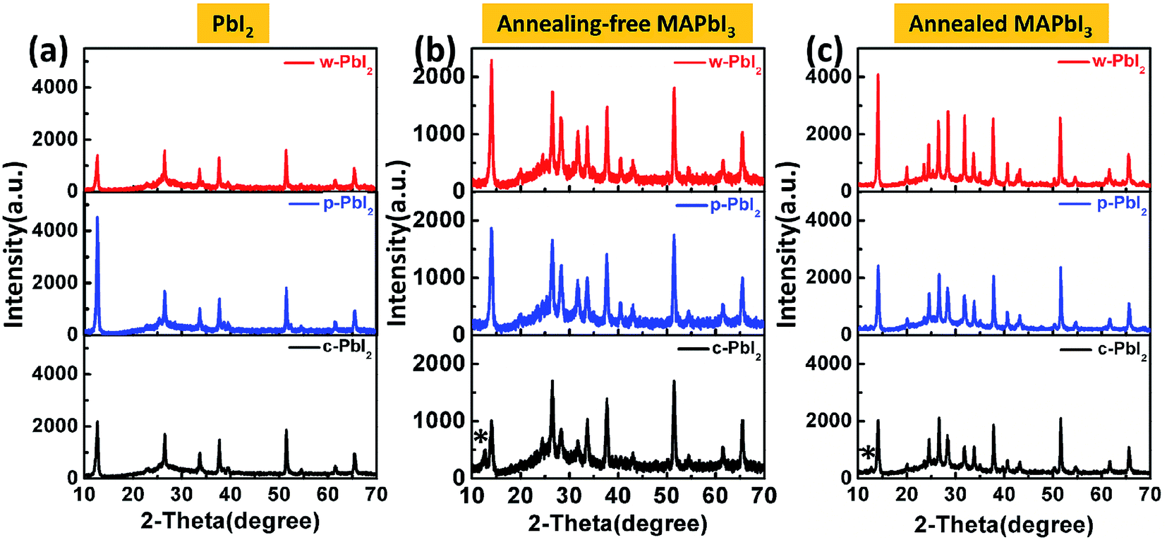 | ||
| Fig. 3 XRD patterns of the various PbI2 precursor films (a), the perovskite films prepared from their respective PbI2 precursor films without thermal annealing (b), and the perovskite films with thermal annealing (c). Asterisks indicate the peaks ascribed to PbI2. | ||
It is well known that for a two-step sequential deposition, the perovskite film quality and morphology greatly depend on the processing of the initial PbI2 film.23,37,42 Thus, we investigated the surface morphology of the perovskites fabricated from various PbI2 films by scanning electron microscopy (SEM). Fig. 4(a–c) shows the typical SEM images of top views of the PbI2 precursor films. In the c-PbI2 case, PbI2 was found to form closely packed layered crystals with hundreds of nanometers due to the improved crystallization after 70 °C annealing. In contrast, the w-PbI2 film has a very different morphology since the presence of the coordinative solvent of DMF, where a much more uniform surface with a small crystal sizes, loose crystals and few pinholes is observed. However, the morphology of the p-PbI2 films becomes coarser, which is consistent with the higher absorption baseline of the p-PbI2 films (Fig. 2(a)). There are also much larger holes distributed on the surface of the films, which result from the fast formation of PbI2 due to the effective extraction of DMF molecules by an anti-solvent of IPA from the as-spin-coated PbI2 film. Fig. 4(d–f) shows the typical SEM images of the annealed MAPbI3 films converted from various PbI2 films after the second dropping step. The surface morphologies of perovskites, including grain size, surface roughness and coverage, that converted from three types of PbI2 precursor film are obviously different. The MAPbI3 perovskite film fabricated by c-PbI2 film shows large variations in crystallite size, with islands of sub-micron size situating all over the surface, which is due to the inhibited intercalation reaction of MAI into closely packed PbI2 crystals skeleton. Although the average thickness of the perovskites seems to be uniform, the presence of these random and disordered structures on the surface (marked by red circles, Fig. 4(d)) increases the possibility of current leakage occurring through the thin HTM layer to the electrode.32,43 In contrast, we are able to produce extremely dense and homogeneous and pinholes-free perovskite films by using an annealing-free, wet PbI2 films (Fig. 4(f)), which benefit from the in situ substitution reaction of coordinative solvent (DMF) molecules by the MAI molecules in low crystallization of w-PbI2 film. The crystal grains of the w-PbI2-based perovskite film are larger than those of the c-PbI2 and p-PbI2-based perovskite film, as shown in Fig. S2 in the ESI.† The average grain size of perovskites prepared from c-PbI2, w-PbI2 and p-PbI2 film are approximately 127, 173 and 149 nm, respectively. However, the MAPbI3 film (Fig. 4(e)) fabricated from p-PbI2 film shows a significantly different morphology of an un-continuous and rough surface, which is due to the non-uniform, rough and macro-porous surface character of p-PbI2 precursor film. A similar result can also be obtained from the SEM images of as-prepared MAPbI3 without annealing (Fig. S3†). The cross-sectional SEM image of perovskites coated on mp-TiO2 shows that the MAPbI3 material is uniformly infiltrated into the mesopores of the TiO2 film (Fig. S1†). The differences in surface morphology of the three films are attributed to the various reaction characteristics between PbI2 films and MAI. The nucleation density is much higher for the films processed from well-crystallized PbI2 film, which tends to form a large amount of relatively small crystals and disordered structures. In contrast, for w-PbI2 film, which reacts with MAI in a slower way due to the low crystallization of PbI2, the low nucleation density at initial step is favourable to form large grains at the later crystallization stage.32 Thus, the PbI2 can efficiently react with MAI by an in situ molecular exchange of DMF molecules with MAI in w-PbI2 films, rather than a reaction of MAI with porous PbI2 film formed by the extraction of DMF molecules.13,24 And, the perovskite films fabricated by w-PbI2 precursor film can retain the uniform and smooth surface of the PbI2 film character. Meanwhile, DMF molecules extracted by IPA “activate” the PbI2 film and facilitate the reaction with MAI, reported in the previous literature.40 Those special phenomena of surface morphologies are also observed in atomic force microscopy (AFM) images, as shown in Fig. S4 in the ESI.† The root-mean-square roughnesses (RMS) of the films were also determined by AFM. The RMS values of perovskites prepared by w-PbI2, p-PbI2 and c-PbI2 are 19.5, 54.1 and 39.9 nm, respectively. The film prepared from w-PbI2 exhibits the lowest surface roughness. In general, a smoother surface is accompanied with a higher surface coverage, which is essential for the high photovoltaic performance of perovskite solar cells.18,36
 | ||
| Fig. 4 Typical SEM images of (a–c) c-PbI2, p-PbI2 and w-PbI2 precursor films, respectively. And (d–f) the corresponding annealed MAPbI3 films prepared from their respective precursor films as indicated. The scale bars are 1 μm. | ||
As we all known, the crystallinity and morphology of the perovskite film determine the photovoltaic performance of the cell device. Generally, non-uniform, pinhole surface causes current leakage and defects cause the increment of trapping sites for carrier recombination. Fig. 5(a) shows the typical photocurrent density–voltage (J–V) curves of MAPbI3 devices fabricated by using different PbI2 precursor films in the same batch under simulated 1 sun illumination. The typical cross-sectional SEM images of the fabricated perovskite solar cell are presented Fig. 5(b). Statistical photovoltaic parameters of all these three types of devices fabricated from various PbI2 precursor films are summarized in Table 1. The data were obtained from 20 individual cells. A correlation between film qualities and the device parameters is observed, as evident from the substantial improvement in photovoltaic performance in device prepared using a w-PbI2 films. In the case of c-PbI2, the device exhibits the PCE of 9.80%, along with a Jsc of 17.90 mA cm−2, Voc of 0.921 V, and FF of 0.594. The cell efficiency increases significantly when w-PbI2 is used. The efficiency for w-PbI2-based cell is increased to 15.28% with a Jsc of 20.63 mA cm−2, Voc of 1.002 V, and FF of 0.739. The efficiency enhancement is largely determined by the increased Jsc value, which can be attributed to the complete conversion of PbI2 into MAPbI3, increased MAPbI3 crystallinity, and light absorption of perovskites and improved film morphologies of perovskites. Especially, the unconverted PbI2 in the MAPbI3 film prepared from c-PbI2 will increase the charge transfer resistance since the unsuitable energy level of PbI2. The poor Voc and FF values for the devices based on c-PbI2 result from the bad morphology of perovskite film, in which the presence of these islands of sub-micron crystallites on the perovskites surface (Fig. 4(d)) increases the number of current leakage paths. However, when p-PbI2 is used, all device parameters are increased comparing with c-PbI2-based device, with a typical Jsc of 19.00 mA cm−2, Voc of 0.979 V, and FF of 0.652, yielding an average efficiency of 12.13%. This is probably due to the complete conversion of PbI2 films and improved crystallinity of perovskites and increased light absorption of perovskite layer. The Voc and FF values for the devices based on w-PbI2 are significantly larger than those of the cells fabricated from p-PbI2 precursor film, which is ascribable to the lack of leakage paths in the homogenous perovskite film in consideration of no PbI2 residue found in the p-PbI2-prepared MAPbI3 film (as XRD in Fig. 1). The increased crystal size in perovskites film prepared from w-PbI2 film can also reduce charge trapping and recombination at grain boundaries, thereby improving the FF and Voc owing to better film formation and hence a reduction in the number of shunting paths.32,43 Additionally, the drop in cell performance is mostly consistent with its much shorter photoluminescence (PL) carrier lifetime and reduced recombination resistance, which is due to a coarser, un-continuous and pinhole perovskites, as the below discussed. Furthermore, the results clearly indicated that the w-PbI2-based devices gave better reproducibility due to their high-quality perovskite layer, whereas the c-PbI2-based devices had a broad distribution of efficiencies (Fig. S5†). The external quantum efficiency (EQE) for the devices are also compared (Fig. 5(c)). The integrated current densities of the devices fabricated from c-PbI2, w-PbI2 and p-PbI2 precursor films, calculated from the EQE spectra, are 17.75, 20.22 and 18.74 mA cm−2, respectively. The integrated Jsc values are consistent with the Jsc value obtained from the J–V curves. The EQE intensity dropped at a wavelength longer than 760 nm. This result is consistent with other literature reports.9 It may be owing to the perovskite film having a strong absorption in the visible spectrum (Fig. 2(d)). The EQE of w-PbI2-based MAPbI3 solar cell has reached up to 80% at a wide spectra range, and is higher than those of cell devices fabricated by c-PbI2 and p-PbI2 precursor film. The optimized PCE of the devices prepared from w-PbI2 film is 15.49% with a Jsc of 20.74 mA cm−2, Voc of 1.004 V, and FF of 0.744, and its Jsc value is consistent with the integrated Jsc values of 20.20 mA cm−2 calculated from EQE spectrum (Fig. S6†). The stable power output of this champion cell is about 15.08%, which is closed to its corresponding maximum efficiency value.
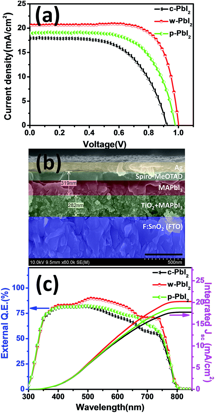 | ||
| Fig. 5 Typical J–V curves (a), cross-sectional SEM image (b) and external quantum efficiency (EQE) (c) of the cell device of MAPbI3 solar cells fabricated from various PbI2 precursor films. The scale bars are 500 nm. | ||
| PbI2 films | Jsca [mA cm−2] | Vocb [V] | FFc | PCEd [%] |
|---|---|---|---|---|
| a Short-circuit photocurrent.b Open-circuit photovoltage.c Fill factor.d Power conversion efficiency. | ||||
| c-PbI2 | 16.61 ± 0.87 (17.72) | 0.941 ± 0.024 (0.958) | 0.625 ± 0.021 (0.616) | 9.76 ± 0.46 (10.45) |
| w-PbI2 | 20.49 ± 0.59 (20.74) | 1.011 ± 0.009 (1.004) | 0.735 ± 0.020 (0.744) | 15.22 ± 0.17 (15.49) |
| p-PbI2 | 17.99 ± 0.75 (18.43) | 0.985 ± 0.013 (0.994) | 0.658 ± 0.020 (0.682) | 11.65 ± 0.45 (12.49) |
The perovskite materials have strong photoluminescence (PL), which is directly associated with the charge recombination. To further reflect the quality of the perovskite films fabricated from various PbI2 film, steady-state PL (SS-PL) and time-resolved PL (TR-PL) decay were characterized, and the corresponding spectra of protective layer (PMMA) coated perovskite films, which were deposited on insulating mesoporous Al2O3 (mp-Al2O3)/glass substrate, are shown in Fig. 6(a). Generally, high-quality perovskite films are associated with high PL efficiency and slow PL decay with reduced non-radiative recombination.4,44 The emission peaks corresponding to the maximum PL intensity are located at about ∼775 nm corresponds to the band gap of about 1.6 eV, which is consistent with the previously reported results.45,46 Several reports have revealed that morphological changes affect the optical properties of the perovskite films. Larger crystallite size induces a smaller band gap and longer lifetime, which is mainly due to the enhancement of the local order of the crystalline structure.46–48 The PL emission peaks of w-PbI2-prepared perovskite film (776 nm) slightly shift to longer wavelength compared with c-PbI2-prepared perovskite film (775 nm). Since the PL of perovskites is expected to occur due to the recombination of localized excitons, the red-shift of PL spectra can be attributed to less localized exciton states in large crystals of w-PbI2-prepared perovskite film (Fig. S2†). w-PbI2-prepared perovskite film shows the highest PL intensity, indicating the non-radiative recombination caused by defects or trapping sites in the film, are greatly suppressed. The TR-PL decays are presented in Fig. 6(b). All curves are well fitted with a double-exponential decay function: I(t) = A1 × exp(−t/τ1) + A2 × exp(−t/τ2), where t is the time after optical excitation, I(t) is the luminescence intensity at time t, A1 and A2 are coefficients, and τ1 and τ2 are the fast and slow decay lifetimes, respectively. Similarly, as obtained from the results of the SS-PL spectra, TR-PL curves clearly show that the PL lifetime is highest for the sample obtained by using w-PbI2 film. The steady PL and TR-PL measurements indicate that the non-radiative recombination channels are effectively inhibited in w-PbI2-based perovskite film. This can be ascribed to the improvement in the crystallization of the perovskite films, the increase in the grain size of perovskites with reduced grain boundaries in the bulk perovskites and the optimization of film morphology. The improved crystallinities size and crystallinity of the perovskite films will decrease the density of the defects and reduce the shunt paths of charge transfer. The crystal quality of perovskites is known to intensely affect the efficiency of photogenerated carrier separation and charge transport.49 It also affects the photovoltaic performance of devices because defects in the crystals create shorting sites and trapping sites for charge recombination.
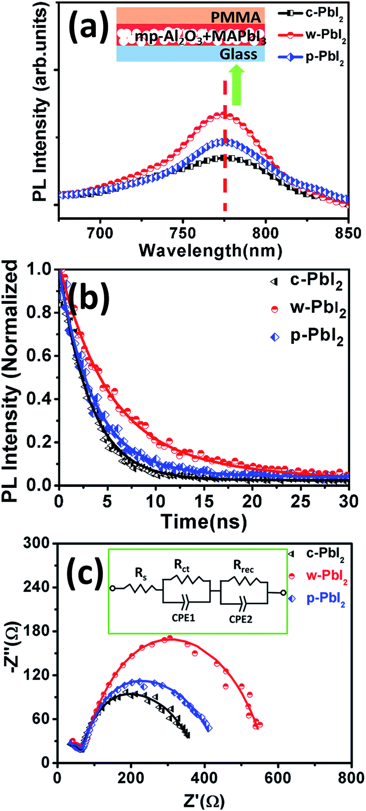 | ||
| Fig. 6 Typical steady-state photoluminescence (PL) spectra (a) and time-resolved PL decay spectra (b) of the perovskite films fabricated from c-PbI2, w-PbI2 and p-PbI2 respectively. Nyquist plots (c) of the devices fabricated from various MAPbI3 films under 1 sun light illumination condition with 0.7 V bias voltage, and the fitted result (solid line) is fitted to experimental data (symbols) using the equivalent circuit for fitting in the inset. | ||
Impedance spectroscopy (IS) can be used to decouple physical processes with various characteristic time scales in solar cells, such as the charge conductivity, carrier recombination resistance, and the chemical capacitance.50–54 In order to deeply understand the variation in the device performance, especially on Voc, Nyquist plots (Fig. 6(c)) of the perovskite solar cells were measured under 1 sun light illumination condition, followed by the method in our previous work.36 The obtained IS spectra only contain a two arcs. As in a previous report,50,53 there is no distinct transmission line behaviour under 1 sun illumination in this experiments. The absence of transmission line behaviour, which results from electron transport resistance, is likely because of the thin TiO2 films employed. As a result, the low electron transport resistance does not allow the sufficient resolution of any transmission line feature. Therefore, the simplified equivalent electrical circuit model is used to fit the experimental data, as shown in Fig. 6(c). The fitted curve is in good agreement with the experimental data. In this equivalent circuit model, the series resistance Rs, representing the ohmic resistance due to wiring, Ag and FTO electrodes measured at high frequency, is equal to the value of high frequency intercept on the real axis. Because of the same device architectures, there is no significantly difference in Rs for various cell devices fabricated from c-PbI2 (15.8 Ω), c-PbI2 (16.6 Ω) and c-PbI2 (16.4 Ω). The high-frequency arc reflects the carrier transport in selective electrodes (SE), which is ascribed to the parallel association of Rct. Rct resistance is influenced by transport resistance at the HTL (spiro-MeOTAD) and ETL (TiO2), but also by the charge transfer resistance at the SE-perovskite interfaces.53–56 In most cases, the current between two different materials undergoes a resistive effect, originating a charge transfer resistance at the interface. As the selective-electrode material (ETL and HTL) and their deposition process are analogous for all samples, we can suppose that Rct is mainly governed by the charge transfer resistance at the HTM-perovskite interface. Moreover, lower Rct has been also obtained for the w-PbI2-based device (48.5 Ω) than those of the c-PbI2-based (58.9 Ω) and c-PbI2-based device (59.1 Ω), which can be attributed to the uniform and ultra-smooth surface of perovskite film prepared from w-PbI2 precursor film. This fact can explain the slightly increased FF of this c-PbI2-based sample in comparison with that of the other samples, as this Rct resistance contributes to the total series resistance. The low-frequency arc represents a recombination process, originating from the parallel association of recombination resistance Rrec, in parallel with a dielectric relaxation capacitance and closely related to the perovskite layer.55–58 The results show that the perovskite solar cell fabricated from w-PbI2 precursor film has a higher Rrec (497.9 Ω) than that of c-PbI2 (264.1 Ω) and p-PbI2 (323.5 Ω), which can be attributed to the increased crystallinity and grain sizes of w-PbI2-prepared perovskites. Consequently, higher Voc observed for w-PbI2-based sample in comparison with that of the others can be unambiguously explained as a result of the lower recombination, resulting from higher recombination resistance. As a result, the cell device fabricated by w-PbI2 precursor film possesses a low Rct and a high Rrec, which indicates its high charge transfer rate and low carrier recombination rate. We confirmed this by TR-PL measurements. Therefore, the perovskite films prepared with w-PbI2 film have a high light absorption, increased crystallinity, and high-quality film morphology, and the devices have a low charge transfer resistance and a high recombination resistance, leading to the enhanced photovoltaic performance.
Conclusions
In summary, we have demonstrated a facile and reproducible approach to obtain high-quality MAPbI3 with excellent photovoltaic performance based on a two-step sequential solution deposition, in which an annealing-free and wet PbI2 film was used as the precursor film. The retarded crystallization and controlled morphology of the annealing-free and wet PbI2 film is favourable to its conversion to MAPbI3, which is due to a direct molecular substitution of DMF molecules intercalated in PbI2 with MAI molecules. Also, the application of the w-PbI2 film is beneficial to improve the crystallinity, surface morphology and the efficiency of light harvesting of the perovskite films, which further reduces the recombination of photogenerated carriers and increases the life times of charge carriers in the fabricated devices. Compared with the control cell device fabricated by a conventional dry and compact PbI2 films, a significant improvement (nearly 56%) in the average PCE is obtained from w-PbI2-based perovskite solar cells. In addition, PCE of best device fabricated by w-PbI2 can reach up to 15.49%, with a high stable power output of 15.08%. Therefore, our present work has highlighted an effective strategy to prepare high-quality perovskite films for high-performance perovskite solar cells.Acknowledgements
This work is supported by the National Natural Science Foundation of China (No. 11474199) and Research Fund of Jiangsu Key Laboratory for Solar Cell Materials and Technology (No. SKLPSTKF201501). Instrumental Analysis Center of Shanghai Jiao Tong University and National Engineering Research Center for Nanotechnology are sincerely acknowledged for assisting relevant analyses.Notes and references
- A. Kojima, K. Teshima, Y. Shirai and T. Miyasaka, J. Am. Chem. Soc., 2009, 131, 6050–6051 CrossRef CAS PubMed.
- D. B. Mitzi, Prog. Inorg. Chem., 1999, 48, 1–121 CrossRef CAS.
- K. Tanaka, T. Takahashi, T. Ban, T. Kondo, K. Uchida and N. Miura, Solid State Commun., 2003, 127, 619–623 CrossRef CAS.
- S. D. Stranks, G. E. Eperon, G. Grancini, C. Menelaou, M. J. Alcocer, T. Leijtens, L. M. Herz, A. Petrozza and H. J. Snaith, Science, 2013, 342, 341–344 CrossRef CAS PubMed.
- J. H. Noh, S. H. Im, J. H. Heo, T. N. Mandal and S. I. Seok, Nano Lett., 2013, 13, 1764–1769 CrossRef CAS PubMed.
- M. R. Filip, G. E. Eperon, H. J. Snaith and F. Giustino, Nat. Commun., 2014, 5, 5757 CrossRef CAS PubMed.
- NREL, Best Research-Cell Efficiencies, http://www.nrel.gov/ncpv/images/efficiency_chart.jpg, accessed September 1, 2016 Search PubMed.
- J. H. Im, I. H. Jang, N. Pellet, M. Grätzel and N. G. Park, Nat. Nanotechnol., 2014, 9, 927–932 CrossRef CAS PubMed.
- H. S. Kim, C. R. Lee, J. H. Im, K. B. Lee, T. Moehl, A. Marchioro, S. J. Moon, R. Humphry-Baker, J. H. Yum, J. E. Moser, M. Grätzel and N. G. Park, Sci. Rep., 2012, 2, 591–597 Search PubMed.
- W. Z. Li, J. D. Fan, J. W. Li, Y. H. Mai and L. D. Wang, J. Am. Chem. Soc., 2015, 137, 10399–10405 CrossRef CAS PubMed.
- D. Liu and T. L. Kelly, Nat. Photonics, 2013, 8, 133–138 CrossRef.
- J. W. Jung, S. T. Williams and A. K. Y. Jen, RSC Adv., 2014, 4, 62971–62977 RSC.
- W. S. Yang, J. H. Noh, N. J. Jeon, Y. C. Kim, S. Ryu, J. Seo and S. I. Seok, Science, 2015, 348, 1234–1237 CrossRef CAS PubMed.
- D. Li, P. Liao, X. Shai, W. Huang, S. Liu, H. Li, Y. Shen and M. Wang, RSC Adv., 2016, 6, 89356–89366 RSC.
- J. Burschka, N. Pellet, S. J. Moon, R. Humphry-Baker, P. Gao, M. K. Nazeeruddin and M. Grätzel, Nature, 2013, 499, 316–319 CrossRef CAS PubMed.
- D. Bi, S. J. Moon, L. Häggman, G. Boschloo, L. Yang, E. M. J. Johansson, M. K. Nazeeruddin, M. Grätzel and A. Hagfeldt, RSC Adv., 2013, 3, 18762–18766 RSC.
- W. Zhang, M. Saliba, D. T. Moore, S. K. Pathak, M. T. Hörantner, T. Stergiopoulos, S. D. Stranks, G. E. Eperon, J. A. Alexander-Webber, A. Abate, A. Sadhanala, S. Yao, Y. Chen, R. H. Friend, L. A. Estroff, U. Wiesner and H. J. Snaith, Nat. Commun., 2015, 6, 6142 CrossRef CAS PubMed.
- N. J. Jeon, J. H. Noh, Y. C. Kim, W. S. Yang, S. Ryu and S. I. Seok, Nat. Mater., 2014, 13, 897–903 CrossRef CAS PubMed.
- Z. M. Zhou, Z. W. Wang, Y. Y. Zhou, S. P. Pang, D. Wang, H. X. Xu, Z. H. Liu, N. P. Padture and G. L. Cui, Angew. Chem., Int. Ed., 2015, 54, 9705–9709 CrossRef CAS PubMed.
- Q. Chen, H. Zhou, Z. Hong, S. Luo, H. S. Duan, H. H. Wang, Y. Liu, G. Li and Y. Yang, J. Am. Chem. Soc., 2014, 136, 622–625 CrossRef CAS PubMed.
- M. Liu, M. B. Johnston and H. J. Snaith, Nature, 2013, 501, 395–398 CrossRef CAS PubMed.
- L. K. Ono, S. Wang, Y. Kato, S. R. Raga and Y. Qi, Energy Environ. Sci., 2014, 7, 3989–3993 CAS.
- T. Y. Zhang, M. J. Yang, Y. X. Zhao and K. Zhu, Nano Lett., 2015, 15, 3959–3963 CrossRef CAS PubMed.
- Y. Z. Wu, A. Islam, X. D. Yang, C. J. Qin, J. Liu, K. Zhang, W. Q. Peng and L. Y. Han, Energy Environ. Sci., 2014, 7, 2934–2938 CAS.
- D. H. Cao, C. C. Stoumpos, C. D. Malliakas, M. J. Katz, O. K. Farha, J. T. Hupp and M. G. Kanatzidis, APL Mater., 2014, 2, 091101 CrossRef.
- B. E. Cohen, S. Gamliel and L. Etgar, APL Mater., 2014, 2, 081502 CrossRef.
- Y. X. Zhao and K. Zhu, J. Mater. Chem. A, 2015, 3, 9086–9091 CAS.
- L. Zheng, Y. Ma, S. Chu, S. Wang, B. Qu, L. Xiao, Z. Chen, Q. Gong, Z. Wu and X. Hou, Nanoscale, 2014, 6, 8171–8176 RSC.
- P. Docampo, F. Hanusch, S. D. Stranks, M. Döblinger, J. M. Feckl, M. Ehrensperger, N. K. Minar, M. B. Johnston, H. J. Snaith and T. Bein, Adv. Energy Mater., 2014, 4, 1400355 CrossRef.
- H. A. Harms, N. Tetreault, N. Pellet, M. Bensimon and M. Grätzel, Faraday Discuss., 2014, 176, 251–269 RSC.
- H. Zheng, W. Wang, S. Yang, Y. Liu and J. Sun, RSC Adv., 2016, 6, 1611–1617 RSC.
- W. Fu, J. Yan, Z. Zhang, T. Ye, Y. Liu, J. Wu, J. Yao, C. Z. Li, H. Li and H. Chen, Sol. Energy Mater. Sol. Cells, 2016, 155, 331–340 CrossRef CAS.
- G. Li, T. Y. Zhang and Y. X. Zhao, J. Mater. Chem. A, 2015, 3, 19674–19678 CAS.
- J. Cao, F. Wang, H. Yu, Y. Zhou, H. Lu, N. Zhao and C.-P. Wong, J. Mater. Chem. A, 2016, 4, 10223–10230 CAS.
- M. Z. Mokhtar, M. Chen, E. Whittaker, B. Hamilton, N. Aristidou, S. Ramadan, A. Gholinia, S. A. Haque, P. O'Brien and B. R. Saunders, Phys. Chem. Chem. Phys., 2017, 19, 7204–7214 RSC.
- C. Y. Sun, Y. P. Guo, B. J. Fang, J. M. Yang, B. Qin, H. N. Duan, Y. J. Chen, H. Li and H. Z. Liu, J. Phys. Chem. C, 2016, 120, 12980–12988 CAS.
- T. H. Liu, Q. Hu, J. Wu, K. Chen, L. C. Zhao, F. Liu, C. Wang, H. Lu, S. Jia, T. Russell, R. Zhu and Q. Gong, Adv. Energy Mater., 2016, 6, 1501890 CrossRef.
- H. N. Chen, X. L. Zheng, Q. Li, Y. L. Yang, S. Xiao, C. Hu, Y. Bai, T. Zhang, K. S. Wong and S. H. Yang, J. Mater. Chem. A, 2016, 4, 12897–12912 CAS.
- X. W. Chang, W. P. Li, H. N. Chen, L. Q. Zhu, H. C. Liu, H. F. Geng, S. S. Xiang, J. M. Liu, X. L. Zheng, Y. Yang and S. H. Yang, ACS Appl. Mater. Interfaces, 2016, 8, 30184–30192 CAS.
- C. Y. Sun, Y. P. Guo, H. N. Duan, Y. J. Chen, Y. L. Guo, H. Li and H. Z. Liu, Sol. Energy Mater. Sol. Cells, 2015, 143, 360–368 CrossRef CAS.
- M. Yang, Y. Zhou, Y. Zeng, C.-S. Jiang, N. P. Padture and K. Zhu, Adv. Mater., 2015, 27, 6363–6370 CrossRef CAS PubMed.
- H. Zhang, J. Mao, H. He, D. Zhang, H. L. Zhu, F. Xie, K. S. Wong, M. Grätzel and W. C. H. Choy, Adv. Energy Mater., 2015, 5, 1501354 CrossRef.
- N. Tripathi, M. Yanagida, Y. Shirai, T. Masuda, L. Han and K. Miyano, J. Mater. Chem. A, 2015, 3, 12081–12088 CAS.
- D. W. deQuilettes, S. M. Vorpahl, S. D. Stranks, H. Nagaoka, G. E. Eperon, M. E. Ziffer, H. J. Snaith and D. S. Ginger, Science, 2015, 348, 683–686 CrossRef CAS PubMed.
- H.-S. Ko, J.-W. Lee and N. G. Park, J. Mater. Chem. A, 2015, 3, 8808–8815 CAS.
- C. Roldan-Carmona, P. Gratia, I. Zimmermann, G. Grancini, P. Gao, M. Graetzel and M. K. Nazeeruddin, Energy Environ. Sci., 2015, 8, 3550–3556 CAS.
- V. D'Innocenzo, A. R. S. Kandada, M. De Bastiani, M. Gandini and A. Petrozza, J. Am. Chem. Soc., 2014, 136, 17730–17733 CrossRef PubMed.
- M. Z. Mokhtar, M. Chen, E. Whittaker, B. Hamilton, N. Aristidou, S. Ramadan, A. Gholinia, S. A. Haque, P. O'Brien and B. R. Saunders, Phys. Chem. Chem. Phys., 2017, 19, 7204–7214 RSC.
- G. Xing, N. Mathews, S. Sun, S. S. Lim, Y. M. Lam, M. Gratzel, S. Mhaisalkar and T. C. Sum, Science, 2013, 342, 344–347 CrossRef CAS PubMed.
- J. A. Christians, R. C. M. Fung and P. V. Kamat, J. Am. Chem. Soc., 2014, 136, 758–764 CrossRef CAS PubMed.
- P. P. Boix, G. Larramona, A. Jacob, B. Delatouche, I. Mora-Sero and J. Bisquert, J. Phys. Chem. C, 2012, 116, 1579–1587 CAS.
- P. P. Boix, Y. H. Lee, F. Fabregat-Santiago, S. H. Im, I. Mora-Sero, J. Bisquert and S. I. Seok, ACS Nano, 2012, 6, 873–880 CrossRef CAS PubMed.
- H. S. Kim, I. Mora-Sero, V. Gonzalez-Pedro, F. Fabregat-Santiago, E. J. Juarez-Perez, N. G. Park and J. Bisquert, Nat. Commun., 2013, 4, 2242 Search PubMed.
- X. Cao, C. Li, Y. Li, F. Fang, X. Cui, Y. Yao and J. Wei, Nanoscale, 2016, 8, 19804–19810 RSC.
- E. J. Juarez-Perez, M. Wuβler, F. Fabregat-Santiago, K. Lakus-Wollny, E. Mankel, T. Mayer, W. Jaegermann and I. Mora-Sero, J. Phys. Chem. Lett., 2014, 5, 680–685 CrossRef CAS PubMed.
- J. Zhang, E. J. Juarez-Perez, I. Mora-Sero, B. Viana and T. Pauporte, J. Mater. Chem. A, 2015, 3, 4909–4915 CAS.
- V. Gonzalez-Pedro, E. J. Juarez-Perez, W. S. Arsyad, E. M. Barea, F. Fabregat-Santiago, I. Mora-Sero and J. Bisquert, Nano Lett., 2014, 14, 888–893 CrossRef CAS PubMed.
- A. Dualeh, T. Moehl, N. Tetreault, J. Teuscher, P. Gao, M. K. Nazeeruddin and M. Grätzel, ACS Nano, 2014, 8, 362–373 CrossRef CAS PubMed.
Footnote |
| † Electronic supplementary information (ESI) available: Cross-sectional SEM images, AFM topographies of perovskite films; J–V curves of the best perovskite solar cell fabricated by w-PbI2 film. See DOI: 10.1039/c7ra03066e |
| This journal is © The Royal Society of Chemistry 2017 |