
 Open Access Article
 This Open Access Article is licensed under a
 Creative Commons Attribution 3.0 Unported Licence
A low-cost, high-efficiency light absorption structure inspired by the Papilio ulysses butterfly
Wanlin Wang a,
Wang Zhang*b,
Di Zhangb and
Guo Ping Wang*a
a,
Wang Zhang*b,
Di Zhangb and
Guo Ping Wang*a
aCollege of Electronic Science and Technology, Guangdong Provincial Key Laboratory of Optoelectronic Micro/Nano Optomechatronics Engineering, Shenzhen University, Shenzhen 518060, China. E-mail: gpwang@szu.edu.cn
bState Key Laboratory of Metal Matrix Composites, Shanghai Jiao Tong University, Shanghai 200240, China. E-mail: wangzhang@sjtu.edu.cn
First published on 26th April 2017
Abstract
The nano-hole array structure in the black scales of the butterfly can be viewed as a natural solar collector. A low-cost, high-efficiency light absorption structure, inspired by the Papilio ulysses butterfly, was optimized using a finite-difference time-domain method. The results show that the nano-hole structure of Papilio ulysses contributes to light absorption. The shape of the holes affects the angular dependence of absorption. The absorption efficiency was found to be strongly affected by three parameters: H (the depth of the hole), D (the thickness of the hole-wall) and L (the size of the hole). These parameters were swept together in numerous simulations. The optimized nano-hole array saves 84% more material than a thin film of equal absorption (90%) at a wavelength of 600 nm.
1. Introduction
The poor infrared absorption of crystalline silicon resulting from its indirect band gap poses a challenge towards its use in solar photovoltaics. Currently, commercial solar cells have 200–300 μm crystalline silicon active layers that efficiently absorb light. This thickness needs to be reduced to several micrometers.1 A thinner active layer has the added advantage of efficient charge-carrier transport. Thus, an effective technique for light trapping in thin active layers needs to be developed.2,3 Various structures employing random or periodical structured surfaces to increase the absorption in thin film photovoltaics have been widely investigated, and an alternative strategy is modify the structure of the active layer itself. Vertically aligned nanorod or nanocone arrays in the active layers have been considered.4,5 Theoretical studies have shown that these structures can improve light absorption.6,7 Han and Chen3 studied a nano-hole array, and their results shows that it required twelve times less silicon by mass to obtain the same ultimate efficiency as a standard 300 μm crystalline silicon wafer. Their calculations3 show that nano-hole arrays are more efficient than nanorods for practical thicknesses. The absorption structure in butterfly scales were also developed as stealth skills,8,9 light trapping schemes,10 infrared absorption11 and thermal sensors.12 Thus, stimulated by the design principles found in nature, super black films were manufactured by imitating a scales microstructure.13,14 Moreover, we studied the disordered structure of Papilio ulysses and discovered their unusually omnidirectional light absorption properties.15The black scales in butterflies can be considered as a structure used to absorb solar energy.11,16–18 Some of the black scales are constructed with ridges and a nano-hole structure. The tapering of the ridges reduces the extent of back-reflection and scattering, while the nano-hole structures enhance the absorption and reduce the amount of material. The periodic arrangements of the ridges and nano-holes lead to a strongly anisotropic angular absorption.15,19 This anisotropic angular absorption was also investigated in this study.
The subfamily Papilioninae is known for its variously colored and large wings, and its strong flight power. Its green band in the dorsal wing has attracted scientists' attention.20,21 Blackness is another important factor in the color of the butterfly as it clearly increases the contrast of the colored wing patterns. The presence of blackness indicates that the visible light of all the wavelengths is absorbed effectively. This particular and elaborate mechanism is necessary to reduce the amount of material and enhance the absorption.16,17,22,23 Vukusic et al.17 measured the nanostructure and absorption spectra of two different levels of blackness. They reported that lattice structures increased the optical path length by multiple scattering on the surface, where the pigments were diffusely distributed. The tapered shape of the ridge was used to decrease the abrupt change in the refractive index on the surface. Zhao et al.16 reported that the periodically aligned inverse-V type ridges with oblique side walls transfer light beams to the nano-hole area where the unique light-trapping effect occurs. The reported study mainly focused on the absorption properties of the special nanostructure. While nature is a brilliant artist with great wisdom, it would be never-ending to study and borrow the art of nature. In a butterfly, the absorption needs to be achieved with a light frame to facilitate the flight. Herein, a new pathway was paved for the extensive exploration of strategies inspired by nature in designing a sophisticated system with low-cost and highly efficient light absorption.
In this study, a nano-hole array inspired by Papilio ulysses was investigated using a finite-difference time-domain (FDTD) method. The optical performance and structure of Papilio ulysses is shown in Fig. 1. Our goal is not to create an exact computational model for this butterfly but to develop the design criteria for a low-cost and highly efficient light absorption structure. Different parameters of the nano-hole array model were investigated, namely the shape of the hole, H (the depth of the hole), D (the thickness of the hole-wall) and L (the size of the hole). These parameters were swept together in numerous simulations. Then, the key factors were optimized using the particle swarm optimization (PSO) method to achieve a low-cost and highly efficient light absorption. The absorption enhancement effects were studied over a range of wavelengths. Our results were obtained in regard to reduced material use through absorption enhancement.
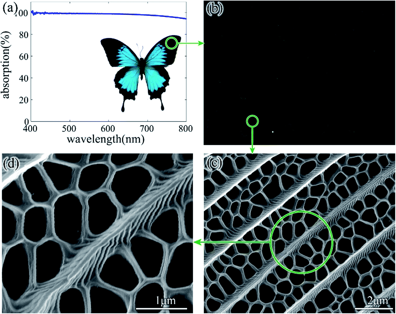 | ||
| Fig. 1 The optical performance and structure of Papilio ulysses. (a) Papilio ulysses and the absorption spectra of its black scales. (b) The microcosmic view of the black scales of Papilio ulysses. (c) and (d) SEM images of the black scales of Papilio ulysses at different magnifications. | ||
2. Method
The nano-hole array of the black scales in Papilio ulysses was investigated using the FDTD method with a three-dimensional model (Fig. 2). Herein, part 2 in Fig. 2 was chosen because this part was considered as the main light-trapping structure, while the other parts (P1, P3 and P4) also contributed a little to the absorption. Thus, the simulation of P2 in this study was lower than the experimental data, as shown in Fig. 1. Structure P2 can be depicted in the x–y plane and z direction, respectively. The lattice in the x–y plane contains different shapes (e.g. rectangle, hexagon, triangle and trapezoid pentagon) according to electron microscopy studies16,17 and the results in Fig. 1. These different shapes are distributed randomly in butterflies. Schematics of the four shapes S1–S4 studied here are shown in Fig. 2(c). The period of the ridge and the filling ratio were fixed at 1380 nm and 24%, respectively in these four shapes. The plane wave was applied in this study. The absorption value was defined as follows: A (absorption) = 1 − R (reflection) − T (transmission).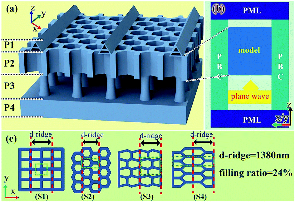 | ||
| Fig. 2 Computational model. (a) Four parts of the black scales in Papilio ulysses. Part 1: the ridges. P2: the nano-hole array structure. P3: the pillars. P4: the substrate. (b) The boundary conditions in the horizontal (x & y) direction are periodic (periodic boundary condition, PBC) and in the vertical (z) direction is absorbing (perfectly matched layer, PML). The plane wave light source illuminates the structure. (c) Four shapes designed for the hole in P2, the period of the ridge and the filling ratio are fixed at 1380 nm and 24%, respectively (the unit cell is shown in the green dashed line box). | ||
The scales of Papilio ulysses comprise chitin and diffused melanin. The refractive index of butterfly chitin has been established to be around 1.56,24 while the refractive index of melanin is much less certain. Because melanin is a strongly absorbing pigment, the value of the refractive index is a complex number, which is difficult to measure accurately. The refractive index of sepia melanin at a wavelength of 633 nm is reported to be (1.655 ± 0.008) + i(0.12 ± 0.07).25 Similar data, equal to 1.55 + i0.14, were reported for the melanin elytra of a buprestid beetle.26 Recently the index values of chitin and melanin in the elytron of the jewel beetle were reported.27 The real part (n) of the high-index layer increases from 1.65 to 1.80 upon decreasing the wavelength. The imaginary part (k) increases to about 0.1 for the shortest wavelength, while for the low-index layer, the real part shows a slight increase from 1.55 to 1.60 and the imaginary part is found to be very small. The index values were also studied in the damselfly.28 The real part of the refractive index at 500 nm for the different cases studied was 1.552 (chitin: dragonfly), 1.580 (immature male), 1.615 (mature female), and 1.663 (mature male). In the beginning of this study, the index value was set at 1.56 + i0.06. Our goal was not to obtain the exact refractive index for Papilio ulysses but to design a light absorption structure inspired by the butterfly. The imaginary part k was set to a small value to make sure that not only melanin but also the structure contributes to the absorption. Then, the imaginary part was set at 0.15 to facilitate the optimization of the structure. This nano-hole array was investigated in detail by sweeping the parameters. The boundary conditions in the vertical (x & y) direction were periodic (periodic boundary condition, PBC) and in the horizontal (z) direction was absorbing (perfectly matched layer, PML), as shown in Fig. 2(b). Periodic boundary conditions reduce the simulation time significantly and make it possible to sweep the parameters. This is the reason we abstracted the complex butterfly structure as a periodic model. The SEM images were obtained using an FEI Sirion 200 field-emission-gun scanning electron microscope. The optical micrographs of the samples were taken using a digital optical microscope (VHX-600, Keyence). The absorption measurements were made using a QDI 2010 UV-vis-near-IR micro-spectrophotometer.
3. Results
3.1. Study parameters: shape, L, D and H
The absorptions with different shapes, H, D and L values were studied under normal incidence as shown in Fig. 3. The H, D and L values represent the hole size, hole-wall thickness and hole depth, respectively. The period of the ridge and the filling ratio were fixed at 1380 nm and 24%, respectively with shapes S1–S4. In addition, the default L, D and H values of S2 were set at 400 nm, 100 nm and 1500 nm, respectively. The absorptions of the different shaped structures (S2–S4) show a slight difference, as illustrated in Fig. 3(a), while the value of shape S1 is smaller than the other three. Thus, the hole shape was not the key factor in the absorption efficiency. In the next section, we show that the shape of the structures affects the angular absorption properties. The absorptions increase with high D and H values and low L values as shown in Fig. 3(b)–(d). The mass per area (mpa) of S2 can be presented as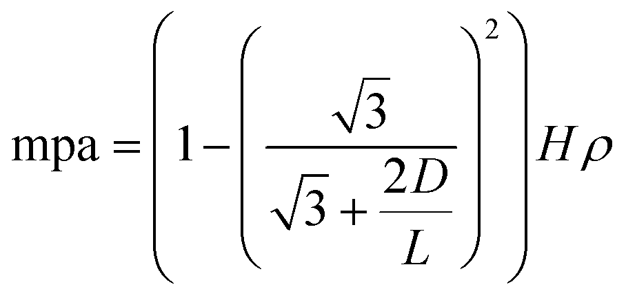 (ρ is the density). The mass per area increases with high D and H values and low L values, and this is agreement with the change in absorption. Thus, it seems that a higher absorption is achieved at the cost of using more material. In order to save the cost and reduce the weight, the nano-hole structure was optimized and is discussed in the following section (sweep parameters).
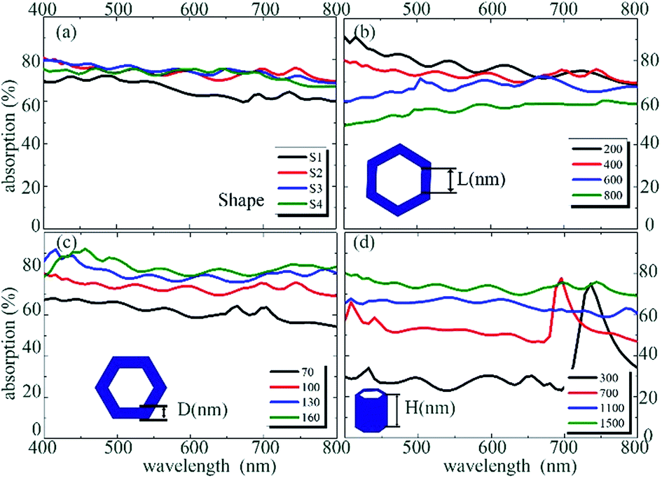 | ||
| Fig. 3 The absorption spectra obtained under normal incidence with: (a) different shapes S1–S4 as shown in Fig. 2(c); (b) different L (hole size) of the side in shape S2, the D and H in this part were set at 100 nm and 1500 nm, respectively; (c) different D (hole-wall thickness) of the side in shape S2, the L and H in this part were set at 400 nm and 1500 nm, respectively; (d) different H (hole depth) of the structure in shape S2, the L and D in this part were set at 400 nm and 100 nm, respectively. A thin layer of substrate was considered in this part with a thickness of 100 nm. | ||
As illustrated in Fig. 4, the absorption was studied using a field map in the x–y plane. Herein, shape S2 was chosen as an example. The simulations were completed with L = 200 nm, L = 800 nm, D = 70 nm and D = 160 nm. Four cross-section field maps were given in four z positions: 1 nm, 500 nm, 1000 nm and 1500 nm. On comparing column D = 70 nm and D = 160 nm we can see that the energy cannot be exhausted if the D value is too small, while with a smaller L value of 200 nm, the energy exhausts quickly. It can also be seen that the energy can be absorbed only if the H(z) value is large enough. Thus, the absorptions increase with high D and H values and low L values, as discussed above.
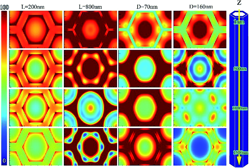 | ||
| Fig. 4 Field map with shape S2 in the x–y plane with different H, L and D values with the wavelength = 600 nm. The parameters are set at L = 200 nm and 800 nm, D = 70 nm and 160 nm and H = 1 nm, 500 nm, 1000 nm and 1500 nm. | ||
3.2. Under various incident angles
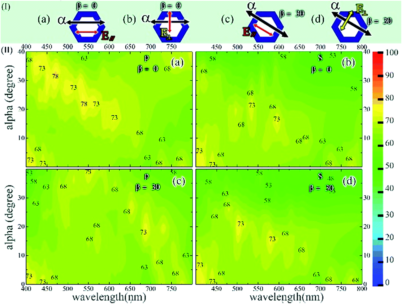
Thus far, the absorption under normal incidence has been studied. Herein, we perform the absorption using broad incident angles. The models used in this part are similar to those used for absorption under normal incidence except that the substrate is neglected here. Fig. 5(I) shows the schematic definition of the incident angle α, polarization and the model. Larger incident angles require more memory. To balance the dilemma, the polar angle α is limited to be between 0° to 40°. Because the structures we chose were symmetrical, the azimuth angle β was set to be the symmetry axis direction, such as 0° and 45° for shape S1, and 0° and 30° for shape S2. The incident plane was defined by β and α. In this part, the L, D, and H values were set at 600 nm, 100 nm and 1500 nm, respectively.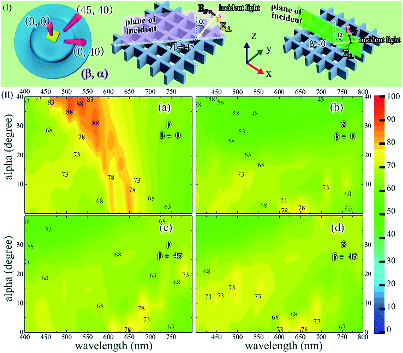 | ||
| Fig. 5 The absorption of shape S1 with different incident angles. (I) The sketch map of the polar angle α and the azimuth angle β, polarization and model S1. (II) The absorption spectra contour plot versus wavelength and α. (a) Under p polarization and β = 0°. (b) Under s polarization and β = 0°. (c) Under p polarization and β = 45°. (d) Under s polarization and β = 45°. | ||
The absorption spectra contour plots of shape S1 versus the wavelength under various incident angles are shown in Fig. 5(II)(a)–(d). The results show that the absorption can be achieved under various incident angles, and the absorption values changed from 43% to 88% with the different α, β and polarizations.
The absorption spectra of shape S2 are shown in Fig. 6. Fig. 6(I) shows the sketch map of the incident angle α, the polarizations and the model. The azimuth angle β was set at 0° and 30° according to the symmetric axis of the hexagon. The values of L, D, and H were set at 400 nm, 100 nm and 1500 nm, respectively. The absorption spectra contour plots of S2 versus the wavelength under various incident angles are shown in Fig. 6(II)(a)–(d). The absorption of S2 was similar to the case of S1, which was also affected by α, β, and the polarizations. However, the absorption of shape S2 was much steadier than S1. The shape of the hole affected the angular dependence of absorption.
 | ||
| Fig. 6 The absorption of shape S2 with different incident angles. (I) The sketch map of the polar angle α and the azimuth angle β, polarization and model S2. (II) The absorption spectra contour plot versus wavelength and α. (a) Under p polarization and β = 0°. (b) Under s polarization and β = 0°. (c) Under p polarization and β = 30°. (d) Under s polarization and β = 30°. | ||
To study the relationship among α, β, polarizations, and absorption, a simple model was investigated as shown in Fig. 7(II)(c) inset. Fig. 7(I) shows the sketch map of the incident angle α, the polarizations, and the model. The azimuth angle β was set at 0° and 90°. The values of D and H were set at 100 nm and 1500 nm, respectively. This model was decomposed by shape S1. The absorption spectra contour plots are shown in Fig. 7(II)(a)–(d). When the electric field was parallel to the plane of the rectangle, as shown in Fig. 7(II)(b)–(c), the absorption was much larger than the opposite condition. When the angle between the incident light and the plane of the rectangle increases, the absorption decreases as shown in Fig. 7(II)(a)–(b). If the incident light was parallel to the plane of the rectangle, the absorption did not decrease with higher incident angles. Hence the absorption was affected by the three parameters: the angle of electric field with the plane of rectangle, the angle between incident light and the plane of rectangle, and the incident angle α.
 | ||
| Fig. 7 The absorption of shape erects rectangle array structure with different incident angles. (I) The sketch map of the polar angle α and the azimuth angle β, polarization and the model. (II) The absorption spectra contour plot versus wavelength and α. (a) Under p polarization and β = 0°. (b) Under s polarization and β = 0°. (c) Under p polarization and β = 90°. The inset of (c) is the model of the rectangle array. (d) Under s polarization and β = 90°. | ||
When two rectangle array models merge into one structure by crossing each other, shape S1 can be obtained. The case shown in Fig. 5(a) can be considered as the merging of Fig. 7(II)(a) and (c) by crossing each other. The case shown in Fig. 5(b) can be considered as the merging of Fig. 7(II)(b) and (d) by crossing each other. Their corresponding absorption spectra also affirm this type of merging. The lobe in Fig. 7(II)(c) can be explained by the lobe in Fig. 5(a). In conclusion, an appropriate shape should be chosen to satisfy the special angle dependent requirements when we design the absorption structure. A highly efficient light absorption structure can be achieved by optimizing parameters D, H and L. Thus, the structure with shape S1 was chosen because the shape was not the key factor for the absorption efficiency, and this simple model can reduce the simulation time significantly. Then, we can sweep the key parameters (D, H and L) over a large range to investigate the absorption efficiency.
3.3. Mass per area
In the discussion above, the refractive index was set at 1.56 + i0.06 to clarify the contribution of the structure to the absorption. It is very difficult to achieve high absorption by merely increasing H with a too low k value. Analogously, it is very difficult to reach high absorption by increasing the k value with a too small H value. Therefore, the k value was set at 0.15 in this part to facilitate the optimization of the light absorption structure. Our goal was to design a light absorption structure, which uses less material to save costs and reduce the weight. Thus, the “mass per area” was taken into account. Herein, when a homogeneous material was assumed, the masssample/Scover (mass per area) = ρsampleVsample/Scover, where Vsample/Scover is used to represent the “mass per area”.The shape of the nano-hole array in the x–y direction was discussed above. Herein, the absorption with different shapes in the z direction is shown in Fig. 8. These four models have the same Vsample/Scover value. Line “a” and line “b” in Fig. 8(II) show that the nano-hole array can enhance the absorption compared with the thin film structure of Fig. 8(a). Line “b” and line “c” in Fig. 8(II) show a similar absorption with a normal hole shape and a gradient hole shape. Line “b” and line “d” in Fig. 8(II) show that the trapezoidal hole structure decreases the absorption compared with the normal hole structure. Thus, the simple rectangle shape (b) was chosen here for the optimization study.
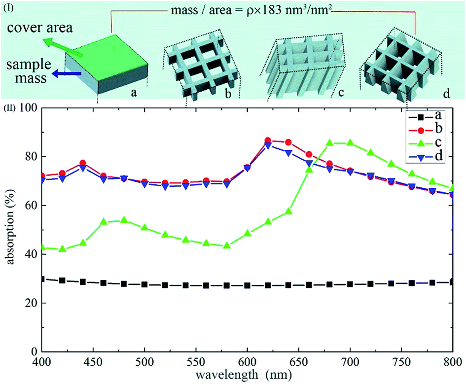 | ||
| Fig. 8 The absorption of the different shapes in the z direction with the same “mass per area”. (I) The sketch map of different shape in the z direction: (a) thin film, (b) rectangle shape, (c) gradient shape and d-trapezoidal shape. Shape (c) and (d) are just a variant of shape (b). (II) The absorption spectra line plot versus wavelength with the different shapes in the z direction. | ||
The L, D, and H values are swept ranging from 400 nm to 800 nm, 300 nm to 700 nm and 60 nm to 180 nm, respectively to search for a structure with high absorption. The cycle graph of these three parameters is shown in Fig. 9(a). Every parameter takes 8 values, and thus in total there are 8 × 8 × 8 = 512 samples. The axis of the abscissa is the sample number. Fig. 9(c) shows the values of L, D, and H for each sample. Fig. 9(b) shows the “mass per area” (Vsample/Scover) for each sample, which is calculated using the L, D, and H values as follows: 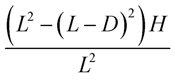 . Thus, when we analyze the absorption of a structure, the corresponding Vsample/Scover value should be considered.
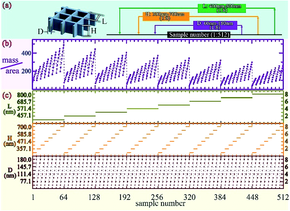 | ||
| Fig. 9 A diagram of the 512 samples by sweeping D, H and L. (a) A sketch map of parameters D, H and L, and the cycle graph. (b) The “mass per area” value for each sample. (c) The D, H and L value for each sample (number 1: D-60 nm, H-300 nm and L-400 nm; number 512: D-180 nm, H-700 nm and L-800 nm). | ||
3.4. Sweep parameters
As shown in Fig. 3, the absorption increases with high D and H values, and low L values. It seems that the higher the absorption achieved, the more the material is used (namely, a higher “mass per area” as shown in Fig. 9). However, our present study wanted to challenge this assumption, demonstrating that some optimized structures contribute to high absorption with a relatively low “mass per area”.Fig. 10 shows the result of sweeping the three parameters (L, D, and H). The conclusion can be summarized as follows: the absorption decreases with an increase in the D value in most samples. However, there are still some samples that have a larger absorption with smaller D values (for example, sample 35–40 with a wavelength of 400 nm, sample 387–390 with wavelength 800 nm). This shows that with samples 441–448 at a wavelength of 800 nm, the absorption is very sensitive to the D value (ΔD: 60 to 180, ΔA: 38% to 90%), whereas with samples 41–48 under a wavelength of 400 nm, the absorption is insensitive to the D value (ΔD: 60 to 180, ΔA: 88% to 94%). Thus, careful choice of the parameters is important for the design of a low-cost and highly efficient light absorption structure.
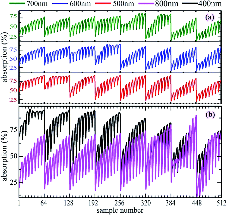 | ||
| Fig. 10 The absorption versus the 512 sample numbers with different wavelengths. (a) Under a wavelength of 500 nm, 600 nm and 700 nm, respectively, and (b) under a wavelength of 400 nm and 800 nm together. | ||
Although most of the samples were sensitive to H, there were a few exceptions. Two examples are given here. Samples (392, 400, …, 440, 448) under a wavelength of 800 nm shows that the absorptions are very sensitive to the H value (ΔH: 300 to 700, ΔA: 42% to 90%), while samples (24, 32, 40, 48, 56, 64) at a wavelength of 400 nm show that the absorptions are very insensitive to the H value (ΔH: 414 to 643, ΔA: 91% to 95%). In addition, the result with the L value was similar with those found for the parameters H and D.
Clearly, the nano-hole array is the absorption structure because of its anti-reflection characteristics. First, the high absorption value can be achieved with a high extinction coefficient. However, this is not the problem we focused on. Second, the absorption value also varies with different structure parameters: the H, D, and L values. Our results show that light absorption can be enhanced by optimizing the H, D, and L values. With equal material (mpa), the optimized structure can achieve the highest absorption compared to the other structures.
3.5. Optimizing the structure using the PSO method
To obtain a high absorption structure, the values of H, D, and L should be selected carefully. The particle swarm optimization (PSO) algorithm, a type of the optimization algorithm, was chosen to overcome this problem. The PSO algorithm, which is inspired from the social behavior of animal species such as birds, bees, and others (particles), was introduced by Eberhart and Kennedy29 while looking for their requirements in their research area. As a robust, stochastic evolutionary strategy, the PSO algorithm has recently been used in solving electromagnetic problems30,31 and has been used to design non-linear and non-continual optimization approaches with continuous variables.Fig. 11 shows the result of the optimization process. The absorption was fixed at 90%. The refractive index was set at 1.56 + i0.15. The models of the nano-hole array and thin film structures are shown in Fig. 11(b). The results show that the material can be reduced significantly at a wavelength of 600 nm (as shown in Fig. 11(a)) and with a broadband spectral range of 400 nm to 800 nm (as shown in Fig. 11(c)). Upon comparison with the thin film structure at a wavelength of 600 nm we obtained a structure (H = 700 nm, L = 560 nm and D = 60 nm) that could reduce the amount of material by 84%. In addition, under the broadband wavelength from 400 nm to 800 nm, we found a structure (H = 780 nm, L = 660 nm and D = 164 nm), which could reduce the amount of material by 59%.
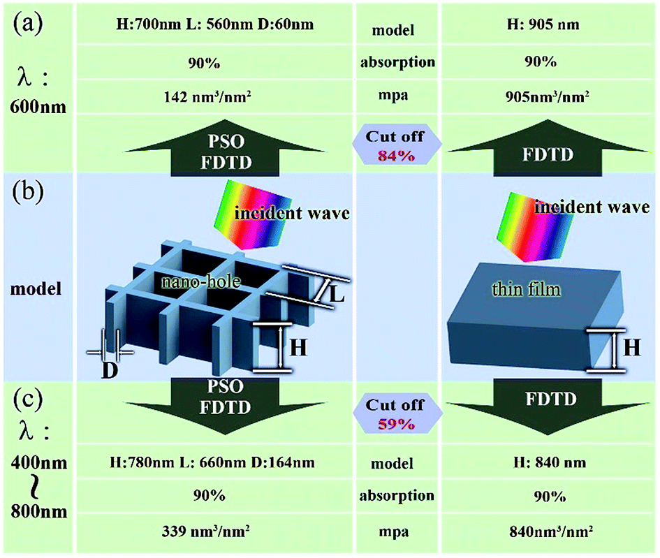 | ||
| Fig. 11 Optimization of the nano-hole array using the PSO algorithm. (a) The optimized results under a wavelength 600 nm in contrast with the thin film structure. (b) The models of the nano-hole array and thin film structure. (c) The optimized results under a broad wavelength range from 400 nm to 800 nm in contrast with the thin film structure. | ||
4. Conclusions
In conclusion, the light absorption properties of the nano-hole array in Papilio ulysses were investigated using the FDTD method. Our results confirmed that the nano-hole structure of Papilio ulysses contributes to the light absorption efficiency. The shape of the hole affects the angular dependence of the absorption, while the parameters H (the depth of the hole), D (the thickness of the hole-wall) and L (the size of the hole) are the key factors affecting the absorption. These three parameters were swept together with numerous simulations. One assumes that a higher absorption requires more material with a higher value for the “mass per area”. However, our studies challenge this assumption, demonstrating that some optimized structures can achieve low-cost and highly efficient light absorption materials. The particle swarm optimization (PSO) algorithm was used for this optimization process. The optimized nano-hole array saves 84% material than a thin film of equal absorption (90%) with a wavelength of 600 nm. While in the wavelength range of 400–800 nm, the optimized nano-hole array saves 59% of the material than a thin film of equal absorption (90%).Acknowledgements
This study was supported by the National Natural Science Foundation of China (Grant No. 51602205, 11274247, 11574218, 11504243 and 11604217), the Natural Science Foundation of Guangdong Province, China (Grant No. 2016A030313042 and 2015A030310400), the Shanghai Rising-Star Program (16QA1402400), the Science and Technology Innovation Commission of Shenzhen (Grant No. JCYJ20160520165724531) and the Fundamental Research Funds for the Shenzhen university (Grant No. 2016025).References
- K. Catchpole and A. Polman, Opt. Express, 2008, 16, 21793–21800 CrossRef CAS PubMed.
- V. E. Ferry, L. A. Sweatlock, D. Pacifici and H. A. Atwater, Nano Lett., 2008, 8, 4391–4397 CrossRef CAS PubMed.
- S. E. Han and G. Chen, Nano Lett., 2010, 10, 1012–1015 CrossRef CAS PubMed.
- B. Tian, X. Zheng, T. J. Kempa, Y. Fang, N. Yu, G. Yu, J. Huang and C. M. Lieber, Nature, 2007, 449, 885–889 CrossRef CAS PubMed.
- Z. Fan, H. Razavi, J.-w. Do, A. Moriwaki, O. Ergen, Y.-L. Chueh, P. W. Leu, J. C. Ho, T. Takahashi and L. A. Reichertz, Nat. Mater., 2009, 8, 648–653 CrossRef CAS PubMed.
- J. Li, H. Yu, S. M. Wong, G. Zhang, X. Sun, P. G.-Q. Lo and D.-L. Kwong, Appl. Phys. Lett., 2009, 95, 033102–033103 CrossRef.
- L. Hu and G. Chen, Nano Lett., 2007, 7, 3249–3252 CrossRef CAS PubMed.
- Z. Han, S. Niu, L. Zhang, Z. Liu and L. Ren, J. Bionic Eng., 2013, 10, 162–169 CrossRef.
- Z. Han, C. Shang, Z. Liu and L. Ren, Nanoscale, 2012, 4, 2879–2883 RSC.
- Z. Han, S. Niu, M. Yang, J. Zhang, W. Yin and L. Ren, Nanoscale, 2013, 5, 8500–8506 RSC.
- J. Tian, W. Zhang, J. Gu, T. Deng and D. Zhang, Nano Energy, 2015, 17, 52–62 CrossRef CAS.
- A. D. Pris, Y. Utturkar, C. Surman, W. G. Morris, A. Vert, S. Zalyubovskiy, T. Deng, H. T. Ghiradella and R. A. Potyrailo, Nat. Photonics, 2012, 6, 195–200 CrossRef CAS.
- Q. B. Zhao, T. X. Fan, J. A. Ding, D. Zhang, Q. X. Guo and M. Kamada, Carbon, 2011, 49, 877–883 CrossRef CAS.
- Z. Jakšić, D. Pantelić, M. Sarajlić, S. Savić-Šević, J. Matović, B. Jelenković, D. Vasiljević-Radović, S. Ćurčić, S. Vuković, V. Pavlović, J. Buha, V. Lačković, M. Labudović-Borović and B. Ćurčić, Opt. Mater., 2013, 35, 1869–1875 CrossRef.
- W. Wang, W. Zhang, X. Fang, Y. Huang, Q. Liu, M. Bai and D. Zhang, Opt. Lett., 2014, 39, 4208–4211 CrossRef PubMed.
- Q. Zhao, X. Guo, T. Fan, J. Ding, D. Zhang and Q. Guo, Soft Matter, 2011, 7, 11433 RSC.
- P. Vukusic, J. R. Sambles and C. R. Lawrence, Proc. R. Soc. B, 2004, 271, S237–S239 CrossRef PubMed.
- J. Tian, W. Zhang, X. Fang, Q. Liu, J. Gu, T. Deng, Y. Wang and D. Zhang, J. Mater. Chem. C, 2015, 3, 1672–1679 RSC.
- M. D. Kelzenberg, S. W. Boettcher, J. A. Petykiewicz, D. B. Turner-Evans, M. C. Putnam, E. L. Warren, J. M. Spurgeon, R. M. Briggs, N. S. Lewis and H. A. Atwater, Nat. Mater., 2010, 9, 239–244 CrossRef CAS PubMed.
- P. Vukusic, R. Sambles, C. Lawrence and G. Wakely, Appl. Opt., 2001, 40, 1116–1125 CrossRef CAS PubMed.
- R. O. Prum, J. Exp. Biol., 2006, 209, 748–765 CrossRef PubMed.
- P. Vukusic and I. Hooper, Science, 2005, 310, 1151 CrossRef CAS PubMed.
- L. Wu, W. Ren, Y. Song, M. Xin, S. Niu and Z. Han, RSC Adv., 2015, 5, 46011–46016 RSC.
- P. Vukusic, J. R. Sambles, C. R. Lawrence and R. J. Wootton, Proc. R. Soc. London, Ser. B, 1999, 266, 1403–1411 CrossRef.
- S. Kurtz, S. Kozikowski and L. Wolfram, J. Invest. Dermatol., 1986, 87, 401 Search PubMed.
- J. A. Noyes, P. Vukusic and I. R. Hooper, Opt. Express, 2007, 15, 4351–4358 CrossRef CAS PubMed.
- S. Yoshioka and S. Kinoshita, Phys. Rev. B: Condens. Matter Mater. Phys., 2011, 83, 051917 Search PubMed.
- D. G. Stavenga, H. L. Leertouwer, T. Hariyama, H. A. De Raedt and B. D. Wilts, PLoS One, 2012, 7, e49743 CAS.
- D. W. Boeringer and D. H. Werner, IEEE Trans. Antennas Propag., 2004, 52, 771–779 CrossRef.
- J. Robinson and Y. Rahmat-Samii, IEEE Trans. Antennas Propag., 2004, 52, 397 CrossRef.
- S. Genovesi, R. Mittra, A. Monorchio and G. Manara, IEEE Antennas Wirel Propag Lett., 2006, 5, 277–279 CrossRef.
| This journal is © The Royal Society of Chemistry 2017 |