
 Open Access Article
 This Open Access Article is licensed under a Creative Commons Attribution-Non Commercial 3.0 Unported Licence
Top-down fabrication of fluorine-doped tin oxide nanopillar substrates for solar water splitting†
Maureen H. Tang‡
 a,
Pongkarn Chakthranont‡b and
Thomas F. Jaramillo*b
a,
Pongkarn Chakthranont‡b and
Thomas F. Jaramillo*b
aDepartment of Chemical and Biological Engineering, Drexel University, 3141 Chestnut Street, Philadelphia, Pennsylvania 19104, USA
bDepartment of Chemical Engineering, Stanford, University, 443 Via Ortega, California 94305, USA. E-mail: jaramillo@stanford.edu
First published on 30th May 2017
Abstract
Because of its high electronic conductivity, electrochemical stability, and optical transparency, fluorine-doped tin oxide (FTO) is a frequently used substrate for photoelectrochemical water splitting (PEC), dye-sensitized solar cells (DSSCs) and other electrocatalytic systems. These applications often require high surface-area substrates, but typical wet-chemical and lithographic approaches to nanostructure this promising material have been limited by the toxic fluorine ion and the resistance of tin oxide to standard chemical etchants. In this work, we develop a novel process to nanostructure commercial FTO by combining nanosphere lithography with argon ion-milling. We show nanostructured FTO with nanopillars of tunable height and diameter. Depositing tungsten oxide with atomic layer deposition on the nanostructured FTO substrate yields a PEC photoanode improvement of 40% over the baseline FTO substrate. The improvement is ascribed mainly to the increased roughness factor achieved by nanostructuring the substrate.
1. Introduction
Coating high-surface-area conductive substrates with thin layers of catalytically active materials is a viable strategy to reduce material costs for active materials while improving their activity and stability for a multitude of electrocatalytic and photoelectrocatalytic reactions, including the oxygen evolution reaction (OER). Such an electrode architecture offers more active sites while maintaining short charge transport distances through catalyst materials. The performance of high surface area electrodes relies on good electron transport between the catalytically active materials and the conductive support, as well as the stability of the conductive support at OER conditions.1 Although the high surface area of nanostructured electrodes enables larger currents and better performance, it can also amplify corrosion rates. Material stability is therefore of even greater importance. Improved stability of conductive supports at the OER potential is necessary to enable the mass adoption of electrolyzers, photoelectrochemical (PEC) water splitting devices, and anodes for electrochemical water purification.2–4 Tin oxide is one of the few support materials that offers stability in an electrochemically corrosive environment and has been investigated as such for polymer electrolyte membrane fuel cells.5 As a wide-bandgap semiconductor, SnO2 must be doped in order to gain electrical conductivity. Although indium-tin oxide (ITO) is the current state-of-the-art transparent conductive oxide (TCO) for solar cells, it is not stable in an oxidizing environment.6 Antimony-doped tin oxide (ATO) has also demonstrated instabilities under extended operation, and the stability is sensitive to synthetic parameters such as annealing time.7,8 Fluorine-doped tin oxide (FTO) has so far exhibited the best stability under oxidizing conditions in acidic and basic environments, and has become the substrate of choice for many electrocatalysis and photoelectrocatalysis studies9–14 on the basis of its good conductivity, stability, and, for PEC applications, high optical transmissivity.FTO coatings have been widely adopted to reduce the emissivity of glass windows for improved building efficiency.15 Coating processes for commercial FTO have been achieved by chemical-vapor-deposition process (CVD), physical vapor deposition, and sputtering.16 Although these methods produces high quality films of low resistance and high optical transmittance, the low roughness of the coatings produced is not ideal for catalysis applications. In contrast, wet-chemical methods such as sol–gel or spray pyrolysis have been used to produce FTO electrodes of high surface area, including nanoparticles,17,18 templated inverse opals,19,20 and nanowires.21–23 Although these structures have demonstrated improved performance over planar samples for DSSC and PEC devices, wet-chemical synthesis routes generally lead to less conductive and less stable TCOs than those synthesized commercially by means of the low-pressure, gas-phase synthesis.24,25 Furthermore, wet chemical routes to FTO generally require the use of the highly toxic fluorine ion.
Recognizing the disadvantages to the wet-chemical syntheses of FTO, we have developed a top-down lithographic approach to create FTO nanopillars. Tin oxide is resistant to many dry-etch chemistries, and there have been few reports on this subject.26–29 Fluorine- and chlorine-based reactive ion etching of SnO2 has been shown to achieve good selectivity with a nickel mask.27 Because chlorine was found to damage the tin oxide, other researchers developed etch processes for SnO2 with hydrogen and an organic gas such as ethanol or acetone.26,28 Patterning studies of FTO are also limited. One approach is the use of traditional photolithography and Cl2/Ar chemistry to etch 150 nm deep channels.29 The conversion efficiency of a DSSC fabricated with the patterned substrate increased from 4.63 to 5.60%. In order to obtain sub-micron lithographic features, nanoimprint lithography and a H2/ethanol reactive ion etch was employed.26 The resulting DSSC demonstrated improved light scattering properties and a 2–5% improvement in internal photon-to-current conversion efficiency. However, the etching selectivity was low, resulting in tapered nanopillars and ridged nanolines.
In this work, we use nanosphere lithography combined with argon ion milling to demonstrate good anisotropy and excellent selectivity. Nanosphere lithography is an inexpensive method for patterning large areas of substrates.30 Our approach produces well-ordered nanopillars with tunable heights and diameters, which enhances surface roughness without sacrificing the conductivity and quality of commercial FTO. We further demonstrate the effectiveness of the FTO nanopillars by fabricating ultrathin WO3 photoanodes for PEC water splitting. WO3 is a well-studied photoanode material with various available synthetic methods, including atomic layer deposition (ALD).31,32 The ALD process is advantageous for a number of applications because it offers atomically controlled thickness and excellent step coverage. Thus, the surface texturing of the FTO nanopillars can be preserved. ALD of WO3 also utilizes relatively non-corrosive precursors, has a fast growth rate, and produces highly active films without the need for any dopants.33 The increased roughness factor of the FTO nanopillars is proven to be advantageous for the ultrathin WO3 photoanode and can be further applied to other photoabsorber and catalyst materials.
2. Experimental
2.1 FTO nanostructuring
A fabrication process flow diagram of the FTO nanopillars is shown in Fig. 1. FTO-coated glass slides (TEC 8, Hartford Glass Co., ∼8 Ω sq−1, 10 mm × 15 mm) were cleaned sequentially in detergent, acetone, and isopropanol (IPA). A 12 nm sacrificial layer of aluminum was then evaporated onto the FTO slides (Innotec ES26C E-Beam Evaporator, Innotec). The Al-coated substrates were then rinsed in IPA, dried, and cleaned in oxygen plasma (March Instruments PX-250, 300 V) for 45 seconds with 5 sccm O2 to remove organic residue and to improve wetting. 120 μL (80 μL cm−2) of a mixture of polystyrene nanospheres (Duke Scientific, 5050A, 10% solids by weight), water, and surfactant (400![[thin space (1/6-em)]](https://www.rsc.org/images/entities/char_2009.gif) :1 by volume of methanol: Triton X-100, Sigma Aldrich) was spin-coated (Brewer Science, CEE 200X) on the substrates to form a monolayer of the hexagonal close packed nanosphere mask. After solution dispersion onto the stationary substrate, the spin-coating program consisted of four stages: (i) wetting the substrate at 0 rpm for 10 s; (ii) spreading the solution at 400 rpm for 5 s with a ramp rate of 100 rpm s−1; (iii) spinning the substrate at 1600 rpm for 60 s with a ramp rate of 400 rpm s−1; and finally (iv) removal of excess liquid from the substrate corners at 2000 rpm for 10 s with a ramp rate of 800 rpm s−1. The mixture compositions for different sphere sizes, modified from literature34,35 are described in Table S1 (ESI†).
:1 by volume of methanol: Triton X-100, Sigma Aldrich) was spin-coated (Brewer Science, CEE 200X) on the substrates to form a monolayer of the hexagonal close packed nanosphere mask. After solution dispersion onto the stationary substrate, the spin-coating program consisted of four stages: (i) wetting the substrate at 0 rpm for 10 s; (ii) spreading the solution at 400 rpm for 5 s with a ramp rate of 100 rpm s−1; (iii) spinning the substrate at 1600 rpm for 60 s with a ramp rate of 400 rpm s−1; and finally (iv) removal of excess liquid from the substrate corners at 2000 rpm for 10 s with a ramp rate of 800 rpm s−1. The mixture compositions for different sphere sizes, modified from literature34,35 are described in Table S1 (ESI†).
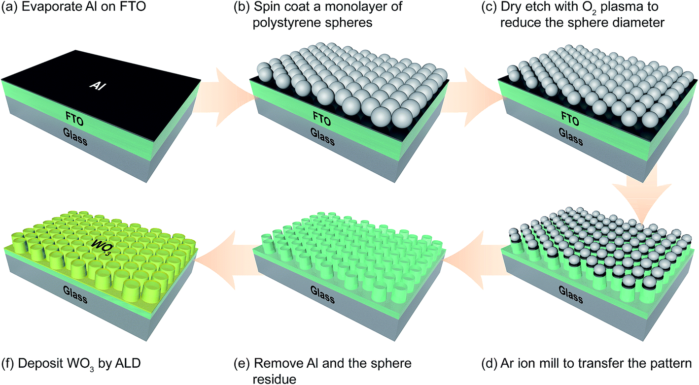 | ||
| Fig. 1 Fabrication process of the WO3 coated FTO nanopillars for the photoelectrochemical water oxidation reaction. (a) A 12 nm sacrificial Al layer is deposited on commercial FTO-coated glass by physical vapor deposition. (b) A monolayer of polystyrene nanospheres (500 or 260 nm in diameter) is formed on the Al layer by spin coating. (c) The nanosphere mask is further reduced in size by dry etching with O2 plasma. (d) FTO columns are formed by anisotropic etching of the FTO substrate with argon ion milling. (e) The mask is then lifted off in 10 M NaOH and cleaned in piranha solution. (f) Lastly, crystalline WO3 is deposited by plasma-assisted atomic layer deposition. | ||
The nanospheres were used as deposited or were reduced in size by exposure to indirect O2 plasma for 60 s (260 nm sphere diameter) or 180 s (500 nm sphere diameter), then mounted on a carrier wafer with Kapton tape and ion-milled for 11 minutes in an Intlvac Nanoquest Research Ion Beam Mill System at 400 V, 50 mA, 15 sccm argon, and 90 degree stage angle. After ion-milling, the polystyrene sphere residues and sacrificial Al were removed by sonication in 10 M NaOH. The substrates were then rinsed in water and cleaned a final time in a piranha solution (3:1 H2SO4:H2O2).
2.2 WO3 photoabsorber synthesis
Prior to WO3 synthesis, the native FTO and FTO nanopillars were cleaned in O2 plasma for 5 minutes to remove any adventitious organics (Drytek Model DRIE-100 Plasma Etcher). 5 Å of Al2O3 was then applied onto the FTO substrates as an adhesion layer (5 cycles of atomic layer deposited Al2O3 at 200 °C). An ultrathin WO3 film was synthesized by atomic layer deposition (ALD) in a Fiji F202 system (Cambridge Nanotech) at 350 °C. An ALD cycle of WO3 consisted of pulsing bis(tert-butylimino)-bis(dimethylamino)tungsten(VI) (BTBMW, Sigma-Aldrich) at 85 °C followed by O2 plasma for 20 s (300 W). The pulse time of BTBMW was varied from 0.1–3 s in order to verify the surface absorption window of the W precursor. The reactor chamber was purged for 20 s with 30 sccm of argon between each precursor pulse. The thickness of ALD tin oxide films grown on silicon wafers was measured by a spectroscopic ellipsometer (Woollam M2000). 20 nm of WO3 was deposited on various FTO substrates and then calcined in a tube furnace at 550 °C in air for 1 hour.2.3 Characterization
The structures and morphologies of the bare FTO nanopillars and the WO3 coated FTO electrodes were imaged using scanning electron microscopy (SEM) (FEI Magellan XHR microscope operated with a beam voltage of 5.0 kV and current of 25 pA). The surface roughness was characterized by atomic force microscopy (AFM) using a Park XE-70 in non-contact mode with Si tip and 37 N m−1 force. The average roughness factor (RF) value, which is a ratio between a true surface area and a geometric surface area, was calculated using the XEI data analysis program. The sheet resistance was measured by a round-tip 4-point probe with 1.0 mm distance between each probe tip. The crystallinity of the WO3 was studied with ambient temperature grazing incidence X-ray diffraction (GIXRD) (Phillips PANanalytical X'Pert Pro) using Cu Kα radiation (λ = 1.54056 Å). The incidence angle (ω) was 0.75° and the attenuator slit was 1/8°. X-ray photoelectron spectroscopy (XPS) was performed using a Phi VersaProbe spectrometer with an Al Kα source. The absorbance was collected inside a custom-fitted integrating sphere (8′′ AdaptaSphere, Labsphere Inc.) with illumination from a 1000 W Xe lamp (Newport-Oriel). The ideal current density was calculated from the absorbance above the band gap, subtracted by the blank substrate absorbance.2.4 Photoelectrochemical testing
All electrochemistry was performed using a BioLogic VSP potentiostat with the EC-Lab software. Capacitance measurements were performed as previously described.36 Cyclic voltammetry was performed in 0.5 M H2SO4 with a platinum counter electrode and Ag/AgCl reference electrode. The electrode potential was swept from 0.05 to 0.15 V vs. reference at scan rates from 50 to 1000 mV s−1, and the capacitive current was obtained by averaging the anodic and cathodic current at 0.10 V vs. Ag/AgCl.A photoelectrode was prepared by contacting a Cu wire to the FTO substrate with conductive paint (Electrodag 502, Ted Pella Inc.) and encasing the contact in insulating epoxy (Loctite Hysol, 9462). The geometric surface areas were measured from photographs with ImageJ software. Photoelectrochemical testing was done in a three-electrode electrochemical setup with a Pt coil counter electrode and a Ag/AgCl (4 M KCl) reference electrode. The electrode was fully submerged in argon-saturated 0.1 M H2SO4 electrolyte (pH 1) in a heart-shaped glass cell (pine) with a flat front-facing window for illumination. The cyclic voltammetry measurements were performed at a 25 mV s−1 scan rate under 2 s chopped illumination from the front side (through the WO3 layer). All the photoelectrochemistry data in this work are reported at the potential vs. RHE scale without iR compensation.
A 1000 W xenon lamp (Newport-Oriel) provided concentrated broadband illumination. The power density of the utilizable photons (wavelength from 280 to 460 nm) was 15.52 mW cm−2, which matches the power density of AM 1.5 G spectrum (ASTM G-173-03) for that same wavelength range. The power was measured by a spectrometer (Jaz, Ocean Optics Inc.).
3. Results and discussion
3.1 Formation of FTO nanopillars
SEM images of the FTO nanopillars at various stages of processing are shown Fig. 2. Fig. 2a and e show the excellent ordering obtained by the spin-coating process. Comparing (a) and (e) reveals that fewer defects are present for the 500 nm spheres, likely because the larger spheres are less influenced by the native roughness of the FTO substrate. Fig. 2b and f show the reduction in sphere size upon exposure to the O2 plasma. The reduction of the sphere size is a critical step for the formation of the pillar structure, as will be further discussed below.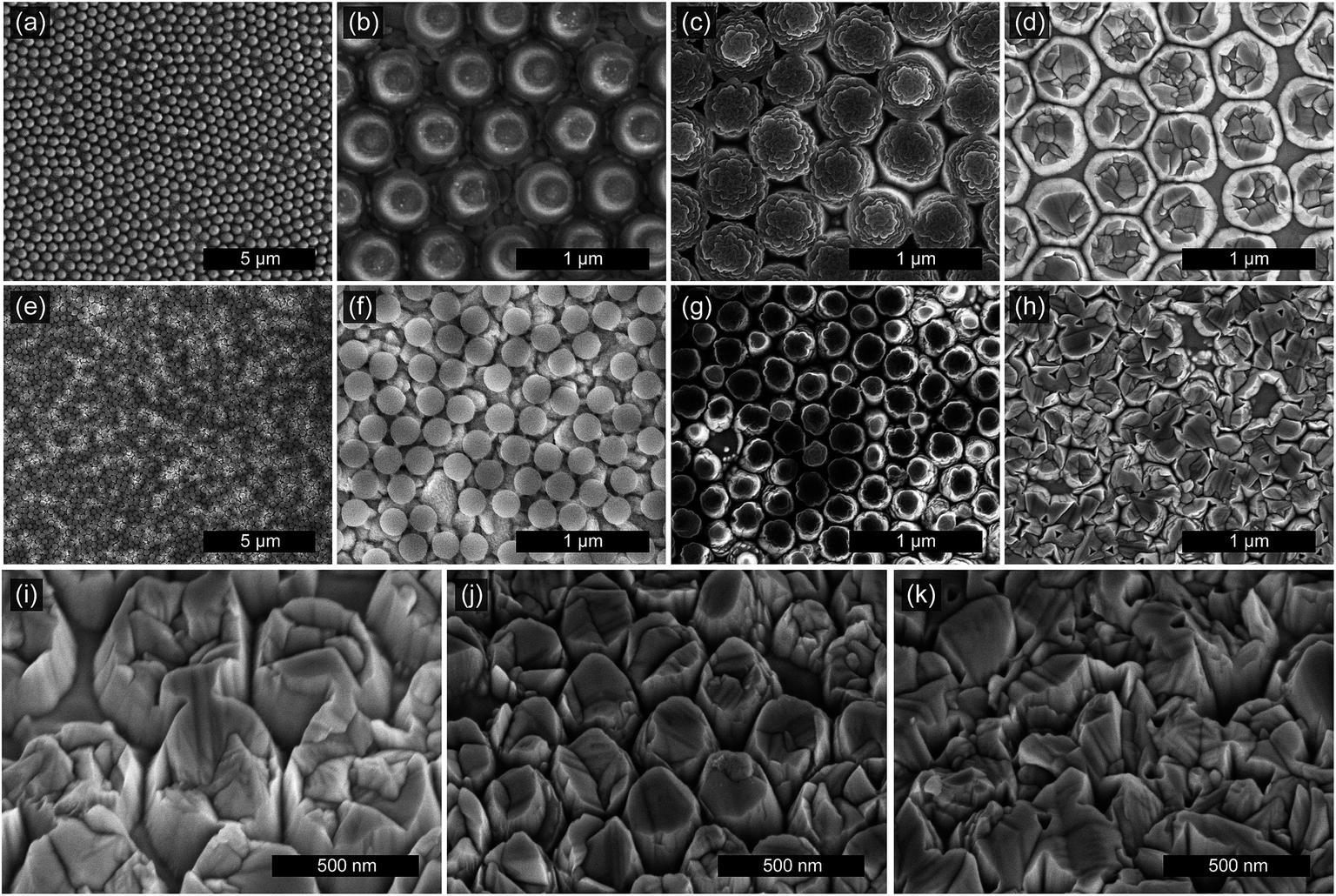 | ||
| Fig. 2 SEM images of the FTO nanopillars at various processing stages using 500 nm spheres (first row) and 260 nm spheres (second row) as patterning masks. (a and e) A monolayer of nanospheres was deposited on FTO substrate by spin-coating. (b and f) The spheres were shrunk in O2 plasma. (c and g) The FTO substrates were milled by argon ion beam. (d and h) After mask removal, nanopillar structures were achieved. 30° tilt and higher magnification SEM images of nanostructured FTO substrates (third row). Reducing the diameters of the (i) 500 nm or (j) 260 nm spheres in O2 plasma prior to milling was necessary to form nanopillars, otherwise only narrow pits are formed between fused spheres, as shown in (k) where no sphere reduction was employed. | ||
Fig. 2c and g demonstrate the anisotropy and selectivity of the ion milling process. Despite etching hundreds of nm deep into the FTO, the feature diameter in Fig. 2c only decreased from 430 to approximately 420 nm. This high Ar-milling selectivity is unique to polystyrene nanospheres and is not observed when using silica or alumina nanospheres as masks. This is because, upon exposure to the argon ions, the polymer becomes highly cross-linked and resistive to further etching, while silica and alumina masks are etched by argon ions at roughly the same rate as the underlying FTO.
Fig. 2d and h show the FTO nanopillars after a mask lift-off process. In the absence of the sacrificial Al layer, we were unable to remove the sphere residues using organic solvents, aggressive oxygen plasmas, calcination, or piranha etchants. However, the deposition of 12 nm of aluminum before spin-coating provides a sacrificial layer that is soluble in strong base. Dissolving the aluminum also lifts off the sphere residues, yielding a clean surface of FTO nanopillars.
Fig. 2i–k show additional SEM images of three samples at 30° tilt and at higher magnification, revealing the importance of reducing sphere diameter in the O2 plasma prior to ion milling. Fig. 2i and j show a different view of the nanopillars formed from 500 nm and 260 nm spheres respectively, consistent with images shown in Fig. 2a–h. If the sphere diameter is not reduced, necking between the spheres limits ion milling to narrow channels, and distinct nanopillars are not formed, as shown in Fig. 2k. We expect that further decreasing the sphere diameter could provide a method to separately tune the nanopillar diameter and spacing, motivating future work. Fig. 2i and j show slight tapering of the nanopillars. This is partly caused by imperfect anisotropy during the milling, but also because initially, the polymer nanospheres have not yet formed the crosslinked network, and the perimeter of the sphere is also milled away. Because the smaller spheres have a higher surface-area-to-volume ratio, this preliminary milling at the edge is relatively more significant and results in lower overall milling selectivity and more tapered nanopillars.
3.2 Roughness factors and optical properties of FTO nanopillars
For PEC, DSSC, and catalysis applications, higher roughness factors are often desired. The roughness factors of the nanostructured FTO substrates were measured using AFM and double-layer capacitance. AFM images are shown in Fig. 3a–c and a representative double-layer capacitance chart is shown in Fig. 3e and f. The resulting roughness factors, normalized to a native FTO, are summarized in Table 1. Good agreement is observed between the two methods of surface area measurement. Also shown in Table 1 is the sheet resistance of different FTO substrates, which only slightly increases with the roughness factor. Although the observed relative roughness factors are relatively small (a factor of 1.4X over native FTO), the etch depth in Fig. 3d is limited not by the selectivity of the mask, but by the thickness of the native FTO. A thicker FTO layer starting material would permit deeper milling and thus a higher roughness factor. FTO that was nanostructured without reducing the sphere diameter exhibits a lower surface area, consistent with the SEM images of interconnected spheres.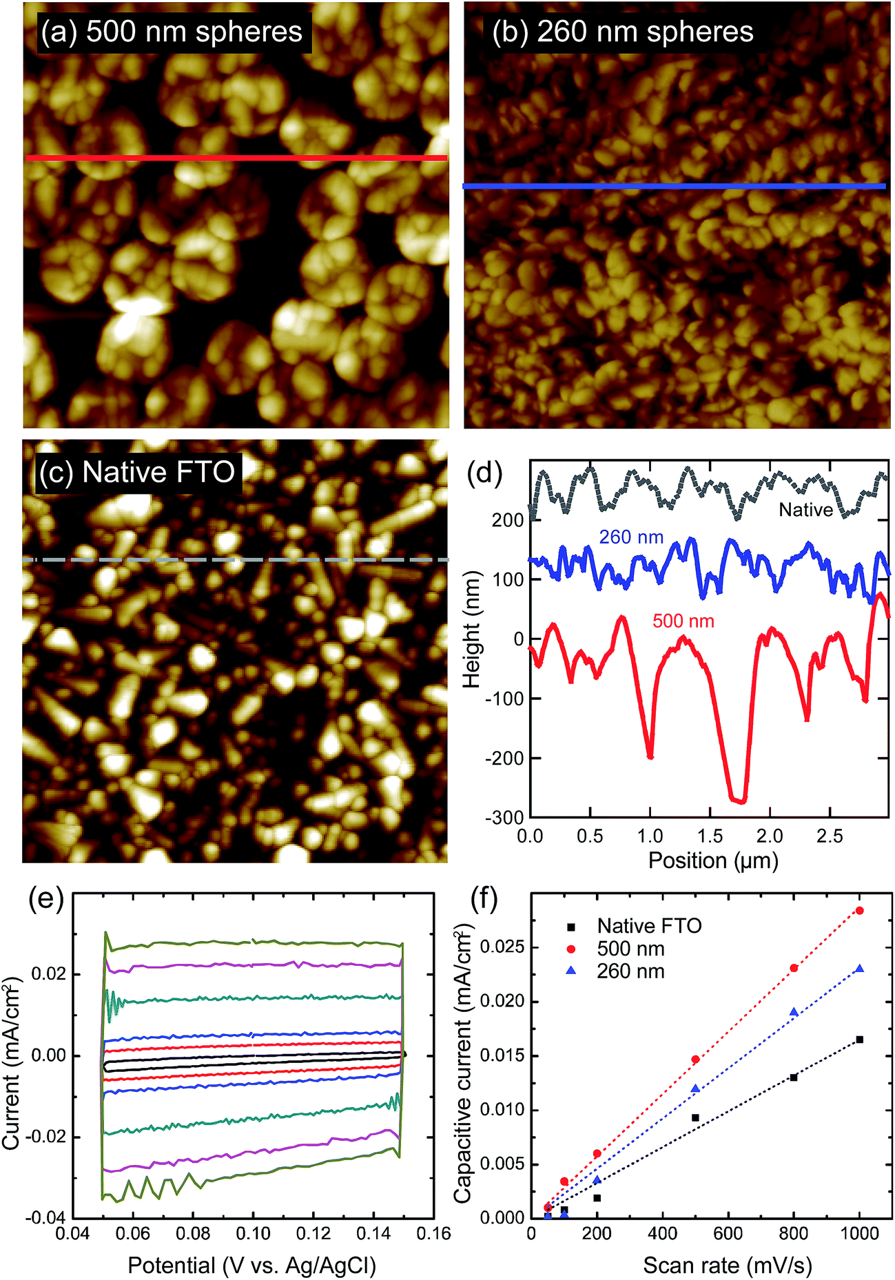 | ||
| Fig. 3 AFM images of the FTO nanopillars: (a) FTO nanopillars formed by 500 nm-sphere mask, (b) 260 nm-sphere mask, and (c) a native FTO. (d) The height measured by AFM conveys the roughness factor of each substrate. (e) Double layer capacitance current densities of 500 nm FTO nanopillars measured by cyclic voltammetry at different scan rates from 50 to 1000 mV s−1. (f) The capacitance current densities extracted from the CVs at 0.10 V vs. Ag/AgCl are linear functions of the scan rate. | ||
| Sample | Normalized RF | Sheet resistance (Ω sq−1) | |
|---|---|---|---|
| AFM | Capacitive current | ||
| Baseline FTO | 1 | 1 | 7.2 |
| 500 nm nanopillars, no sphere reduction | 1.2 | 1.3 | 8.2 |
| 500 nm nanopillars, sphere reduction | 1.2 | 1.4 | 10.0 |
| 260 nm nanopillars, no sphere reduction | 1.0 | 1.3 | 9.6 |
| 260 nm nanopillars, sphere reduction | 1.1 | 1.2 | 9.3 |
For PEC applications, substrates must also be optically transparent. UV-vis absorbance of the nanostructured FTO, as shown in Fig. 4, does not result in significant increases in absorption after the texturing process.
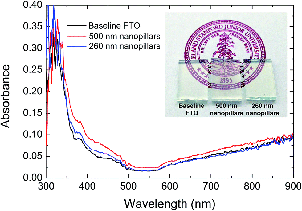 | ||
| Fig. 4 UV-vis absorbance of native FTO substrate and FTO nanopillars. | ||
3.3 WO3 ALD characterizations
Before coating the FTO nanopillars, the ALD WO3 process was investigated on Si planar substrates to determine the surface saturation regime and to verify a linear growth rate. A BTBMW pulse time of 2 s was chosen to ensure high coverage of the W precursor on the substrate surface, resulting in the WO3 growth rate of 0.9 Å per cycle (Fig. S1†). XRD patterns show that the as-deposited ALD WO3 film exhibits an orthorhombic structure, and the post-annealed film is converted to monoclinic WO3 (Fig. 5a), similar to active WO3 reported in literature.33 XPS spectra confirm that the surface of the films consist of WO3 with a carbon content typical of adventitious sources (Fig. 5b).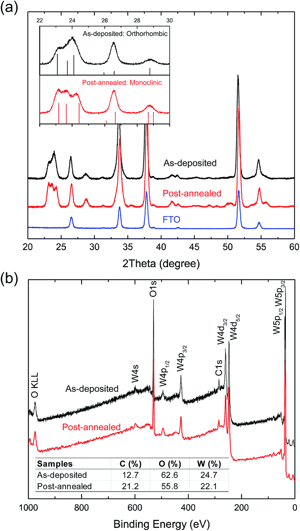 | ||
| Fig. 5 GIXRD and XPS spectra of ALD WO3. (a) GIXRD patterns and (b) XPS spectra of the as-deposited and post-annealed ALD WO3 show that the films consist of crystalline WO3. | ||
3.4 PEC performance
Fig. 6a shows the PEC performance of 20 nm thick WO3 photoanodes. All the WO3-coated FTO nanopillar samples exhibit higher photocurrent density than the equivalent WO3 coated onto a native FTO electrode. The highest photocurrent density was achieved with nanopillar substrates fabricated with 500 nm diameter nanospheres reduced in oxygen plasma for 180 s, a 40% improvement over the use of a native FTO substrate.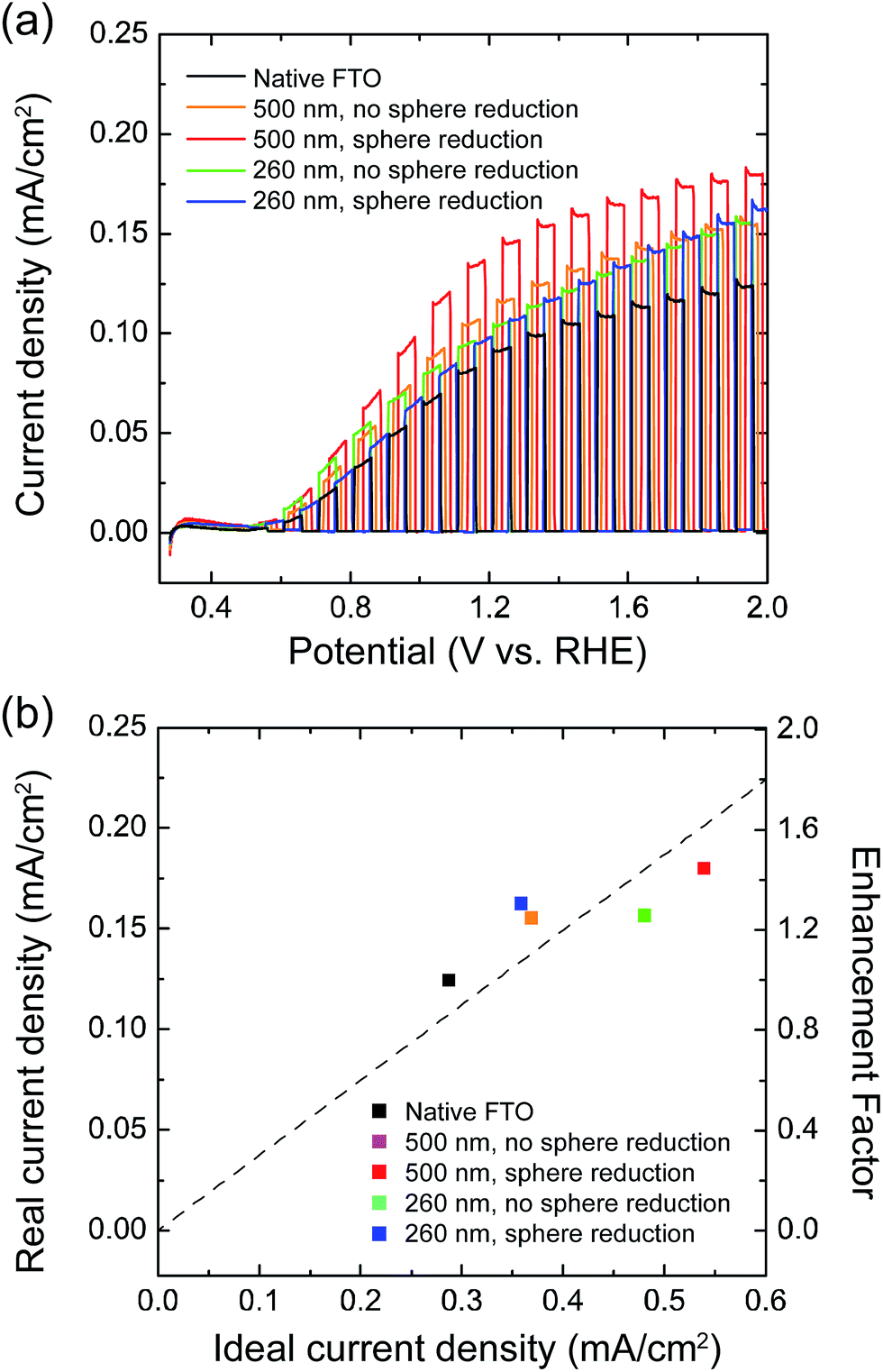 | ||
| Fig. 6 Photoelectrochemical performances ALD WO3 on FTO nanopillars. (a) Photoelectrochemical performance of 20 nm WO3 photoanodes on various FTO substrates under chopped 1-sun illumination. (b) The real current density at 2 V vs. RHE and the photocurrent enhancement factor (WO3 on native FTO = 1) vs. the ideal current density calculated from the absorption. | ||
Fig. 6b shows that the current density (at 2 V vs. RHE) increases linearly with the ideal current density calculated from absorption properties, which indicates direct use of the increased material deposited with no apparent loss from charge transport. Because the current density enhancement factors on nanostructured FTO substrates are similar to their roughness factors reported in Table 1, we can conclude that the increased roughness is the primary cause for this performance enhancement. The proportionate relationship of roughness factor and current enhancement factor implies that the interfacial recombination is not a performance limiting factor because of the negligible change in the substrate quality and the relatively low roughness factor. To improve the PEC performance even further, a thicker native FTO could be used to for higher aspect ratio structures with greater roughness factors.
4. Conclusion
FTO nanopillars were successfully fabricated using a top-down fabrication process consisting of nanosphere lithography and argon ion milling. By varying the sphere size, the sphere reduction time, and the milling duration, the profile and the roughness factor of the FTO nanopillars can be tuned. These FTO nanopillars exhibit the desired properties of excellent ordering, low optical absorption, and low sheet resistivity. The nanopillars were used as a transparent conductive substrate for an ultrathin WO3 PEC electrode synthesized by plasma-assisted ALD. Although the enhanced roughness factor of the FTO nanopillars was limited by the thickness of the starting film of FTO, it was proven to be beneficial for the WO3 photoanode; the enhancement in photocurrent was found to be equal to the increase in roughness factor of the substrate. This result demonstrates that the FTO nanopillars can increase the optical density of the absorber material while maintaining short charge transport distances. Our top-down approach to nanostructuring enhances the roughness factor on commercial FTO without sacrificing the high quality of the substrate, and can be readily generalized for other commercially available conductive substrates and other photoabsorber materials for a variety of applications.Acknowledgements
This paper presents results from an NSF project (award number CBET-1433442) competitively-selected under the solicitation “NSF 14-15: NSF/DOE Partnership on Advanced Frontiers in Renewable Hydrogen Fuel Production via Solar Water Splitting Technologies”, which was co-sponsored by the National Science Foundation, Division of Chemical, Bioengineering, Environmental, and Transport Systems (CBET), and the U.S. Department of Energy, Office of Energy Efficiency and Renewable Energy, Fuel Cell Technologies Office. The authors would like to thank Dr Blaise Pinaud, Ieva Narkeviciute, Dr Michelle Rincon, and Dr J Provine for helpful discussions.References
- J. Moir, N. Soheilnia, P. O'Brien, A. Jelle, C. M. Grozea, D. Faulkner, M. G. Helander and G. A. Ozin, ACS Nano, 2013, 7, 4261–4274 CrossRef CAS PubMed.
- Z. Zhang, J. Liu, J. Gu, L. Su and L. Cheng, Energy Environ. Sci., 2014, 7, 2535–2558 CAS.
- M. G. Walter, E. L. Warren, J. R. McKone, S. W. Boettcher, Q. Mi, E. A. Santori and N. S. Lewis, Chem. Rev., 2010, 110, 6446–6473 CrossRef CAS PubMed.
- B. P. Chaplin, Environ. Sci.: Processes Impacts, 2014, 16, 1182–1203 CAS.
- Y. Shao, J. Liu, Y. Wang and Y. Lin, J. Mater. Chem., 2008, 19, 46–59 RSC.
- J. D. Benck, B. A. Pinaud, Y. Gorlin and T. F. Jaramillo, PLoS One, 2014, 9, e107942 Search PubMed.
- Q. Peng, B. Kalanyan, P. G. Hoertz, A. Miller, D. H. Kim, K. Hanson, L. Alibabaei, J. Liu, T. J. Meyer and G. N. Parsons, Nano Lett., 2013, 13, 1481–1488 CrossRef CAS PubMed.
- E. Fabbri, A. Rabis, R. Kotz and T. J. Schmidt, Phys. Chem. Chem. Phys., 2014, 16, 13672–13681 RSC.
- Y. Liang, T. Tsubota, L. P. A. Mooij and R. van de Krol, J. Phys. Chem. C, 2011, 115, 17594–17598 CAS.
- Y. J. Hwang, C. Hahn, B. Liu and P. Yang, ACS Nano, 2012, 6, 5060–5069 CrossRef CAS PubMed.
- R. Brimblecombe, A. Koo, G. C. Dismukes, G. F. Swiegers and L. Spiccia, J. Am. Chem. Soc., 2010, 132, 2892–2894 CrossRef CAS PubMed.
- G. K. Mor, H. E. Prakasam, O. K. Varghese, K. Shankar and C. A. Grimes, Nano Lett., 2007, 7, 2356–2364 CrossRef CAS PubMed.
- T. Hoshikawa, M. Yamada, R. Kikuchi and K. Eguchi, J. Electrochem. Soc., 2005, 152, E68–E73 CrossRef CAS.
- J. J. Concepcion, J. W. Jurss, M. K. Brennaman, P. G. Hoertz, A. O. T. Patrocinio, N. Y. Murakami Iha, J. L. Templeton and T. J. Meyer, Acc. Chem. Res., 2009, 42, 1954–1965 CrossRef CAS PubMed.
- Pilkington Group Limited, Energy Saving Glass - Warm Coatings, http://www.pilkington.com/pilkington-information/about+pilkington/education/glass+in+buildings/coatings.htm, accessed Jan 18, 2017.
- B. Stjerna, E. Olsson and C. Granqvist, J. Appl. Phys., 1994, 76, 3797–3817 CrossRef CAS.
- T. P. Chou, Q. Zhang, B. Russo and G. Cao, J. Nanophotonics, 2008, 2, 023511 CrossRef.
- Z. Yang, S. Gao, T. Li, F.-Q. Liu, Y. Ren and T. Xu, ACS Appl. Mater. Interfaces, 2012, 4, 4419–4427 CAS.
- J. Xiao, L. Yang, Y. Luo, D. Li and Q. Meng, J. Mater. Chem. C, 2013, 1, 5450–5453 RSC.
- Z. Yang, S. Gao, W. Li, V. Vlasko-Vlasov, U. Welp, W.-K. Kwok and T. Xu, ACS Appl. Mater. Interfaces, 2011, 3, 1101–1108 CAS.
- B. Russo and G. Cao, Appl. Phys. A, 2008, 90, 311–315 CrossRef CAS.
- K. Murakami, A. Bandara, M. Okuya, M. Shimomura and R. M. G. Rajapakse, Synthesis and characterization of one-dimensional nanostructured fluorine-doped tin dioxide thin films, Proc. SPIE 9929, Nanostructured Thin Films IX, 99290X, 2016 Search PubMed.
- A. Bandara, K. Murakami, R. M. G. Rajapakse, P. V. V. Jayaweera, M. Shimomura, H. M. N. Bandara, D. Liyanage and E. V. A. Premalal, Thin Solid Films, 2017, 621, 229–239 CrossRef CAS.
- T. Minami, Semicond. Sci. Technol., 2005, 20, S35 CrossRef CAS.
- H. Bisht, H.-T. Eun, A. Mehrtens and M. Aegerter, Thin Solid Films, 1999, 351, 109–114 CrossRef CAS.
- F. Wang, N. K. Subbaiyan, Q. Wang, C. Rochford, G. Xu, R. Lu, A. Elliot, F. D'Souza, R. Hui and J. Wu, ACS Appl. Mater. Interfaces, 2012, 4, 1565–1572 CAS.
- J. C. Park, J. K. Kim, T. G. Kim, D. W. Lee, H. Cho, H. S. Kim, S. J. Yoon and Y.-G. Jung, Int. J. Mod. Phys. B, 2011, 25, 4237–4240 CrossRef CAS.
- T. Minami, T. Miyata, A. Iwamoto, S. Takata and H. Nanto, Jpn. J. Appl. Phys., Part 2, 1988, 27, L1753 CrossRef CAS.
- S. M. Kong, Y. Xiao, K. H. Kim, W. I. Lee and C. W. Chung, Thin Solid Films, 2011, 519, 3173–3176 CrossRef CAS.
- C. L. Haynes and R. P. Van Duyne, J. Phys. Chem. B, 2001, 105, 5599–5611 CrossRef CAS.
- X. Liu, F. Wang and Q. Wang, Phys. Chem. Chem. Phys., 2012, 14, 7894–7911 RSC.
- J. Malm, T. Sajavaara and M. Karppinen, Chem. Vap. Deposition, 2012, 18, 245–248 CrossRef CAS.
- R. Liu, Y. Lin, L. Y. Chou, S. W. Sheehan, W. He, F. Zhang, H. J. Hou and D. Wang, Angew. Chem., 2011, 123, 519–522 CrossRef.
- C. L. Cheung, R. Nikolić, C. Reinhardt and T. Wang, Nanotechnology, 2006, 17, 1339 CrossRef CAS.
- B. A. Pinaud, Fundamental studies for the design of tantalum nitride photoanodes for solar water splitting, Stanford University, 2013 Search PubMed.
- A. J. Forman, Z. Chen, P. Chakthranont and T. F. Jaramillo, Chem. Mater., 2014, 26, 958–964 CrossRef CAS.
Footnotes |
| † Electronic supplementary information (ESI) available. See DOI: 10.1039/c7ra02937c |
| ‡ ORCID: 0000-0003-0037-4814These two authors contribute equally to this work. |
| This journal is © The Royal Society of Chemistry 2017 |