
 Open Access Article
 This Open Access Article is licensed under a
 Creative Commons Attribution 3.0 Unported Licence
The effect and nature of N–H complexes in the control of the dominant photoluminescence transitions in UV-hydrogenated GaInNAs
C. R. Brown a,
N. J. Estesa,
V. R. Whitesidea,
B. Wangb,
K. Hossainc,
T. D. Goldingc,
M. Lerouxd,
M. Al Khalfiouid,
J. G. Tischlere,
C. T. Ellise,
E. R. Glasere and
I. R. Sellers*a
a,
N. J. Estesa,
V. R. Whitesidea,
B. Wangb,
K. Hossainc,
T. D. Goldingc,
M. Lerouxd,
M. Al Khalfiouid,
J. G. Tischlere,
C. T. Ellise,
E. R. Glasere and
I. R. Sellers*a
aHomer L. Dodge Department of Physics & Astronomy, University of Oklahoma, Norman, Oklahoma 73019, USA. E-mail: sellers@ou.edu
bSchool of Chemical, Biological and Materials Engineering, University of Oklahoma, Norman, Oklahoma 73019, USA
cAmethyst Research Inc., 123 Case Circle, Ardmore, Oklahoma 73401, USA
dCRHEA-CNRS, Rue Bernard Gregory, Valbonne, France
eU.S. Naval Research Laboratory, 455 Overlook Ave SW, Washington D.C. 20375, USA
First published on 11th May 2017
Abstract
Due to its 1 eV band gap and GaAs-matched lattice constant, GaInNAs has long been considered for use in four-junction multi-junction solar cells; but, material quality issues have impeded its use in highly efficient devices. Here, we present an analysis of GaInNAs samples partially hydrogenated via a UV-activated process in which nitrogen-related alloy fluctuations, impurities, and defects have been passivated; remarkably, removing completely the ‘s-shape’ dependence of the photoluminescence while keeping intact the effects of nitrogen substitution, i.e., the band gap of the alloy prior to passivation. Hydrogenation of the optical samples by a UV-activated process has resulted in GaInNAs photoluminescence dominated by the free-excitonic band gap transition, rather than radiative recombination processes from the shallow localized centers that result due to unavoidable alloy fluctuations. This behavior is unique since these centers dominate the low temperature photoluminescence even in the highest quality dilute nitrides. Density functional theory calculations show that the hydrogenation of the N and Ga atoms eliminates the defect levels from the band gap through the formation of H–N centers that act as donors; while at high concentration of hydrogen, Ga–H2–N complexes reside within the continuum. The formation of these hydrogen complexes, along with the incumbent change of the band structure, explains the reduction of emission from the localized centers upon hydrogenation.
1 Introduction
The physical and electrical properties of InGaAs are altered significantly with the introduction of small amounts of nitrogen into the lattice. Notably, it is possible to grow GaInNAs such that it exhibits a band gap of 1 eV with a lattice constant matched to GaAs.1 These properties make GaInNAs appealing for use in four-junction multi-junction solar cells (MJSCs).2 Nevertheless, the short minority carrier diffusion length of dilute nitride materials has impeded their large-scale implementation in high-efficiency photovoltaic devices.3Material quality problems arise in part due to non-idealities during the growth process and the formation of gallium vacancies upon the incorporation of nitrogen into these materials.4 Since the temperature required for ideal InGaAs growth conditions produces phase separation when introducing nitrogen, their growth is typically performed at relatively low temperatures, and with careful control of the III/V flux ratio.5 This results in large nitrogen-related defects such as Ga–N4 and Ga–In–N3 (ref. 6) that are detrimental for solar cells.7
Rapid thermal annealing (RTA) in a nitrogen rich environment has been shown to passivate defects associated with the non-ideal growth conditions: increasing N–As substitution, reducing the density of vacancies and interstitials, and facilitating the rearrangement of nearest neighbors from Ga–N to the more favorable In–N configuration.4,8–11 Time resolved measurements of RTA samples show a nearly twofold increase in the PL decay time compared to as grown material, which corresponds to a large reduction in nonradiative recombination rate.12 However, RTA cannot remove all defects and inhomogeneities, some larger N–N clusters and alloy fluctuations remain.6,13–15 Additionally, laser annealing has also been observed to improve material quality in GaNAs quantum wells and to a much lesser degree in quaternary GaInNAs.16 This effect is neglected here since the effects of laser annealing are irreversible and would produce a permanent change to the PL spectra. This is not evident in the material system studied here, as shown in Fig. 5. Moreover, regardless of material quality, nitrogen–arsenic substitution results in the formation of isoelectronic impurities that have locally distinct electrical properties due to the relatively small size and high electronegativity of nitrogen.17
The formation of single nitrogen centers or clusters of such isoelectronic impurities18 are an intrinsic property of these systems and as such is present even in the highest quality dilute nitrides. In dilute GaAsN single nitrogen centers result in localized states that reside within the continuum of the conduction band, while nearest neighbor N–N pairs and larger nitrogen clusters have been observed below the band gap.19,20 Similar behavior is also observed in GaInNAs.21,22 The presence of these N-based isoelectronic impurities close to, and in resonance with, the conduction band minima results in an unexpected lowering of the band gap in Ga(In,N)As systems. This occurs due to the interaction of, and subsequent repulsion between, the conduction band states and localized states associated with resonant NAs isoelectronic impurities in the alloy.23 In addition, alloy fluctuations driven by indium segregation are also problematic in GaInNAs.9–11 The presence of indium rich regions in the material serve to mimic quantum dots that localize photogenerated carriers at low temperature9,11 increasing the efficiency of radiative recombination; while, decreasing the carrier diffusion length and lifetime.13 These properties – coupled with the presence of deeper donor or acceptor related defects due to N–N clusters – have the dual effect of increasing the potential to improve the radiative efficiency of optical emitters, while inhibiting carrier collection in photodetectors and solar cells. As a result, dilute nitride solar cells have traditionally suffered from poor quantum efficiencies.3,7,13,24
The effects of hydrogenation have been studied extensively in dilute nitride materials as a means of passivating deleterious nitrogen-based defects and impurities; however, previous research has found that hydrogenation has the effect of removing the effect of substitutional nitrogen25 and to stabilize gallium vacancies.26,27 Upon formation of strong H–N complexes, the band gap redshift induced in the III–V with substitutional nitrogen is effectively reversed upon hydrogenation.21 This is observed in the photoluminescence (PL) with a blueshift of the band gap back to that of the nitrogen-free alloy.25
Moreover, in MOCVD grown samples, excess hydrogen has been observed to change the background impurity concentration from p-type – due to the presence of gallium vacancies – to n-type.28 This p- to n-type conversion has been attributed to the formation of stable H–N complexes that act as donors in GaAsN and GaInNAs, in contrast to the strongly amphoteric nature of H in most other III–V semiconductors.24,25 The complete removal of the effects of (nitrogen-related) defects and impurity centers upon hydrogenation is unique to the dilute nitrides. Indeed, such saturation – or complete removal – of defects is not typically observed in other III–V systems, or the well-studied silicon system. Furthermore, the reversibility of this process when the system is subjected to high temperatures is also unique, resulting in the breaking of H–N bonds and a return to the properties of the original GaInNAs material.6
The interesting effects observed upon the hydrogenation of dilute nitrides have been described extensively in the literature.25,29 However, the removal of the associated ‘s-shape’ dependence of the photoluminescence energy as a function of temperature has only been reported recently;22,26,30 most unusual is the control of the effects of shallow localized centers related to alloy fluctuations. In these works, it was shown that not only could deep defects be passivated by careful regulation of the hydrogen concentration; but, it is possible to also control – through the formation of N–H complexes – the prevalence and radiative efficiency of localized states due to indium fluctuations. Having the ability to control the radiative efficiency of the centers is unique since these centers are difficult to remove and typically dominate the low temperature PL in dilute nitrides.
Here, the role of hydrogen in controlling the nature of the photoluminescence is taken further and more explicitly investigated through variable temperature and power dependent PL: these experiments are supported by complementary DFT calculations that are used to predict the most probable role of hydrogen in passivating localization centers. It is shown that with increasing hydrogen concentration that larger molecular N–H2 complexes form. These complexes push into and reside energetically within the continuum; as such, the formation of these centers serves to detune the low energy alloy related transitions, removing their role in photoluminescence.
2 Experimental details
The three samples studied consisted of a 1 μm-thick Ga0.91In0.1N0.03As0.97 layer (composition determined using a calibration epilayer) grown by molecular beam epitaxy at 420 °C on a GaAs substrate and capped by a 75 nm GaAs layer (see Fig. 1(a)). A radio frequency plasma source (ADDON) was used to generate nitrogen radicals from high-purity (6N5) N2 gas. A 550 nm GaAs buffer was also deposited at 580 °C prior to growth of the GaInNAs film. The samples were first annealed post-growth in high-nitrogen conditions at 800 °C for 30 seconds. This temperature was selected based on an annealing study to maximize the PL signal.31 After annealing, one piece – the reference sample – is left unhydrogenated; two of the samples were then hydrogenated using a UV-activated process32 at dosages of 0.5 × 10¹⁵ atoms per cm2 (“intermediate”) and 1.1 × 10¹⁵ atoms per cm2 (“highest”), respectively. | ||
| Fig. 1 (a) Schematic of GaInNAs double heterostructure sample (b) qualitative energy location of localized states due to alloy fluctuations (Eloc) (dashed lines). (c) Example PL spectrum at 4 K of the unhydrogenated reference sample showing two main peaks: at the band gap (EG) and the localized states (Eloc). | ||
The UV-activated process involves the use of energetic photons to irradiate the surface of a material in the presence of hydrogen. Since hydrogen is a non-polar molecule, the UV light does not dissociate hydrogen in the gas phase, but can at the surface; therefore, only the irradiated portions of the surface are hydrogenated. In addition, since the photon energy is less than the ionization energy of hydrogen, photon-activated dissociation of molecular hydrogen yields only neutral atomic hydrogen. Lastly, the process ambient is not constrained to lower pressures but can range from very low pressure (<10−6 Torr) to high pressure (∼100 atmospheres). The conditions for the hydrogenation process used were: excitation wavelength < 325 nm, pressure = 42 Torr, time = 4 h, temperature = 330 °C and 382 °C, for the intermediate and highest dosages, respectively. Analysis of the hydrogen penetration using ion beam analysis indicated a penetration depth of 2 μm; therefore, hydrogenation throughout the whole of the nitride layer. The samples placed in a closed-cycle cryostat were excited with an Ar+ laser at 532 nm and the PL spectra were detected using a LN2-cooled InGaAs array.
3 Results
The 4.2 K PL spectra of the reference sample is shown in Fig. 1(c); there are two main overlapping features: the low energy, slightly more intense peak is associated with carriers localized at states related to alloy fluctuations (Eloc); while, the higher energy (shorter wavelength) peak is attributed to the fundamental band gap transition of the GaInNAs (EG). A schematic of the bands with the approximate position in energy of the localized transitions related to indium based alloy fluctuations (Eloc) (dashed blue line) is shown in Fig. 1(b). Thermopower measurements qualitatively indicate that the samples are weakly p-type, as expected for nominally undoped GaInNAs; this is attributed to the prevalence of gallium vacancies resulting from the non-optimum (low) growth temperatures used to facilitate nitrogen incorporation in these systems. The PL feature ED will be discussed later.Fig. 2(a) shows the temperature-dependent spectra of the reference sample plotted on a log scale. As previously discussed, it exhibits two overlapping peaks characteristic of the band gap (EG) and QD-like localized states (Eloc). At low temperature, the luminescence is dominated by the lower energy Eloc transition. As the temperature increases, carriers gain enough thermal energy to escape and redistribute in the material; thus the PL transitions to emission dominated by the higher energy EG at T > 40 K. This behavior is more clearly demonstrated in the inset to Fig. 2(a), which shows a magnified image of the peaks observed in the main panel of this figure.
 | ||
| Fig. 2 (a) PL spectra for reference sample from 4–300 K. Inset: Magnification of the PL spectra at low temperatures (T < 100 K) reveals marked diminution in peak at (Eloc) with increasing T. The small dip at 1075 nm is an artifact due to a grating response. (b) Energy of the highest intensity feature in each PL spectrum as a function of temperature for the different excitation powers. P0 corresponds to 13 kW cm−2. | ||
When the peak energy of this PL at each temperature is extracted and plotted versus temperature as in Fig. 2(b), the transition from PL dominated by localized states (Eloc) to that dominated by free carrier emission is evident in the ‘s-shape’ temperature dependence typical of these materials.33 This behavior derives from the fact that photogenerated carriers are frozen at local potential minima, transferring to a higher energy state upon increasing thermal excitation. This is illustrated by the change in PL energy at 25 K in Fig. 2(b). At T > 25 K the carriers gain enough thermal energy to escape the localized potential and the free carriers redistribute in the bands of the GaInNAs; the effect of localization is limited at T > 40 K.
Fig. 2(b) also shows the effect of this carrier redistribution for increasing excitation power. At the lowest power (closed circles) the PL spectra show the presence of a (20 meV) deep localization potential observed below 25 K. The photogenerated carriers are readily localized and trapped at these centers for T < 25 K. As the power is increased from intermediate (0.1P0) to the highest power (P0) of 13 kW cm−2, the depth of this localization decreases and the temperature minimum shifts to a slightly lower value; this behavior is indicative of localized state filling upon increasing carrier excitation and occupation.34–36 The blueshift in the minima of the ‘s-shape’ profile reflects increasing occupation of the states. As the temperature is increased the thermal activation and redistribution of the carriers screens the effects of the localized emission; at T > 40 K the energy dependence of the peak PL follows the typical Varshni-type37 band gap dependence with increasing temperature.
Fig. 3(a and b) shows the power and temperature dependent PL spectra and associated peak energy for the ‘highest’ hydrogenated sample. This sample also exhibits a feature related to carriers localized in alloy fluctuations (Eloc) that resides beneath the band gap; but, whose intensity has been lowered to the point where the band gap transition (EG) becomes the dominant (most intense) luminescence even at low temperatures (see inset to Fig. 3(a)). Power-dependent measurements of this sample reveal some re-emergence of the ‘s-shape’ dependence at low temperature and intensity; indicating that the hydrogen dose used (1015 cm−2) is not high enough to produce complete passivation of all defects in the sample.
 | ||
| Fig. 3 (a) PL spectra for highest hydrogenated sample as a function of temperature, no attenuation. Inset: Magnification of the PL spectra at low temperatures (T < 100 K). (b) Re-emergence of the s-shape temperature dependence with decreasing excitation intensity. P0 corresponds to 13 kW cm−2. | ||
In order to properly characterize the features observed in the PL spectra, the individual peaks for all three samples were tracked as a function of attenuation, or excitation power, as shown in Fig. 4 and 5. Gaussian fitting was used to de-convolute the spectra; error bars on the order of the symbol size indicate the quality of the fits as shown in Fig. 4 and 5. Fitting of the peak intensities as a function of power to a power function k(I ∝ Pk) yields the values shown in the graphs. The fitting parameter k falls within one of two regimes according to the dominant recombination center or mechanism: wherein k < 1 is indicative of defect-related states; 1 < k < 2 indicates the recombination is excitonic in nature.34,38
 | ||
| Fig. 4 (a) PL spectra for the reference sample with several excitation powers. (b) Log plot of tracked peak intensities as a function of attenuation. Error bars included are on the order of the symbol size. (c) Energy of tracked peaks, T = 4.2 K. Norm. incident power of 1 corresponds to 13 kW cm−2. | ||
 | ||
| Fig. 5 (a) PL spectra for highest hydrogenated sample at several excitation powers. (b) Log plot of tracked peak intensity, as a function of attenuation. Error bars included are on the order of the symbol size. Peak behavior with attenuation is similar to that of the reference. (c) Energy of tracked peaks. T = 4.2 K. Norm. incident power of 1 corresponds to 13 kW cm−2. | ||
The effect of increasing absolute excitation power from ∼13 W cm−2 to ∼13 kW cm−2 for the reference sample at 4.2 K is shown in Fig. 4(a–c). Fig. 4(a) shows the increasing contribution of the band gap transition (EG) with increasing power. This behavior likely reflects the increased occupation of the finite concentration of localized states in the layer; as well as, the different capture cross-sections for the photogenerated carriers associated with the EG and Eloc radiative recombination processes as the power increases. At 4.2 K despite the increased contribution of (EG), transition (Eloc) still dominates at the highest power in the reference sample. Fig. 4(b) shows the integrated peak intensity versus power for the individual peaks extracted from Gaussian fits of Fig. 4(a) on a log–log plot. This is then used to extract k-values for each of the transitions. The extracted k-values of kG = 1.59 and kloc = 0.95 confirm their origin as the transitions associated with the fundamental GaInNAs band gap and localized states, respectively.
Fig. 4(c) shows the extracted peak energy dependence of the transitions in Fig. 4(a) as a function of power at 4.2 K. In all cases, there is an increase in the energy of the transitions with increasing power. Such blueshifts in energy with power may indicate type-II behavior.39,40 However, the GaInNAs samples investigated are type-I systems. So, this behavior is more likely caused by a combination of local heating, state filling effects and/or spatial separation of the carriers from alloy fluctuations.22,30 Evidence for state filling is observed in Fig. 2(b), where the filling of localized states increases the energy of the resultant PL, which agrees with the simultaneous increase in the localized state transition (Eloc) in Fig. 4(b). The role of alloy fluctuations in spatially separating photogenerated electrons and holes is a well-known effect in GaInNAs systems;22 previously, this effect has been shown to inhibit solar cell operation.13
Fig. 5 shows the effect of excitation power on the ‘highest’ hydrogenated sample at 4.2 K. At the highest excitation density, the PL is dominated by the band gap transition (EG). However, as the excitation power is decreased, the occupation of sub-gap localized states (Eloc) is no longer saturated; these lower energy transitions dominate the PL at lower powers and temperatures. Extraction of the k-parameter for this sample through the linear fit of the log intensity versus log power plot shown in Fig. 5(b) reveals values of kG = 1.75 and kloc = 0.90 for the fundamental band gap and localized states related to alloy fluctuations, respectively. These values are consistent with those extracted for the same transitions determined in the reference sample (see Fig. 4(b)), indicating that these transitions are of the same origin in both samples.
Both reference and hydrogenated samples exhibit a lower energy feature at approximately 1120 nm labeled peak (ED) in Fig. 4(a) and 5(a). Although the exact nature of this feature requires further investigation, several recent works in these systems have shown that larger N–N clusters41–43 result in deep donor and/or acceptor defect states that serve as non-radiative centers at elevated temperatures.11 Such centers are located at energies consistent with their binding energy and serve as deleterious mid-gap states at higher temperature. Since ED is relatively unaffected by temperature, it is consistent with a defect center associated with nitrogen clusters in the material – the origin of these deep donor/acceptor states.
ED has qualitatively similar behavior in that the extracted k-value is less than 1, and (within errors) the same in each sample, kD(ref) = 0.57 and kD(hyd) = 0.51. The extracted k-value (k < 1) for ED confirms its origin as related to a lower energy impurity or defect state. Interestingly, however, ED appears not to be significantly affected by hydrogenation; which is inconsistent with the selective passivation and removal of lower energy states associated with large nitrogen clusters as has been observed previously in these systems.29
Indeed, the resolution of ED actually improves upon hydrogenation (see Fig. 6(b)). The relative insensitivity of the energy of this feature to excitation power (see Fig. 4(c) and 5(c)) and its similarity to that of EG in this regard, suggests this ED is intimately related to the bulk GaInNAs. One potential reason for the apparent non-hydrogen passivation of these states may relate to their physical position in the GaInNAs. Recently, it has been shown that the hydrogen concentration upon UV-assisted hydrogenation in these samples has a non-uniform depth profile, the concentration of which decreases with increasing depth in the structure. Since most of the strain and homogeneities in the quaternary likely occurs close to the GaAs/GaInNAs interface due to the high strain fields at this surface, a lack of defect passivation may indicate a higher defect to hydrogen concentration ratio deeper within the GaInNAs film. Additional studies are now underway to further illuminate this point.
 | ||
| Fig. 6 (a) Comparison of peak energies for each sample vs. temperature at full power (P0). (b) Superposition of PL spectra for reference and highest hydrogenated samples at 4 K and (c) 200 K. | ||
Alternative explanations to the origin of ED are: first, that this feature is related to a donor–acceptor or electron–acceptor transition in the (unintentionally) p-type GaInNAs investigated here. This hypothesis derives from the fact that a strong conduction band (CB) to acceptor impurity transition has been observed previously in p-type GaInNAs grown by MBE.44 This transition was evident 42 meV below the conduction band, which is much deeper than observed in GaAs;45 yet at 4.2 K, consistent with the position (1130 nm) of ED in Fig. 4(a) and 5(a). The second alternative is that this transition is LO-phonon related, which is supported by the constant energy separation between EG and ED (∼40–50 meV), which may suggest a LO-phonon related resonance (i.e. 2LO).46
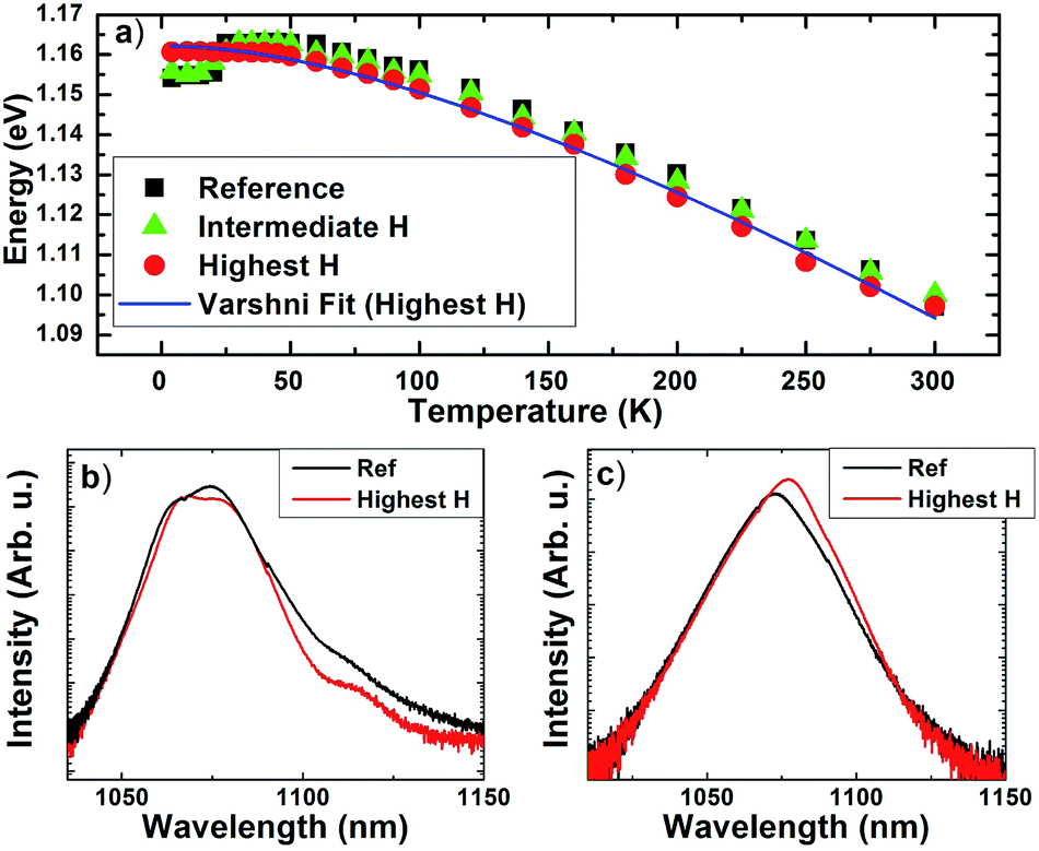
Fig. 6 shows a comparison of the temperature dependent PL energy for the reference (black squares) and ‘highest’ hydrogenated sample (red circles); along with a ‘intermediate’ hydrogenated sample (green triangles). At power P0 the free band-to-band transition in the GaInNAs dominates the PL above 30 K, with the peak energy following that of a conventional semiconductor (Varshni-behavior).37 As the hydrogenation dosage is increased from the reference – to 0.5 × 1015 cm−2 (intermediate) – to 1.1 × 1015 cm−2 (highest) – the ‘s-shape’ is systematically reduced; such that, it is removed at the highest hydrogenation dosage – leading to the dominance of the band gap PL in this sample as discussed above.
Interestingly, as the hydrogen dose is increased, the peak PL energy of the band gap transition (T > 25 K) decreases from ∼1.164 eV for reference sample (black squares) to ∼1.160 eV for the sample subjected to the highest hydrogen concentration (red circles). This reduction in the energy of the GaInNAs band gap with increasing hydrogenation likely reflects the effect of the formation of N–H complexes that relax the tensile strain induced by the presence of the N in the GaInNAs alloy.21 This process occurs through the displacement of the Ga-atoms and the subsequent expansion of the Ga–N bond, all of which results in a redshift in the band gap energy after hydrogenation.26 Although the out-diffusion of nitrogen and/or indium from the alloy upon hydrogenation cannot be completely discounted, the effect of this process would be to increase the energy of the GaInNAs; which is not the case here.
The effect of hydrogen passivation on the relative PL intensity for the samples is shown more in Fig. 6(b) and (c). These spectra show a direct comparison of the PL intensities for the reference (black curve) and highest hydrogenated (red curve) samples at 4.2 K and 200 K, respectively. The intensity of the reference sample is slightly larger than that of the hydrogenated sample at 4.2 K, while slightly less at 200 K. This behavior is consistent with the localized nature of the carriers in the reference sample; i.e., the dominance of radiative recombination processes for photogenerated carriers localized at alloy fluctuations at low temperatures. In the case of the hydrogenated samples, the localization of the carriers is weaker – increasing the spatial diffusion of the carriers, particularly, at higher temperatures; which decreases the radiative recombination rate of the excitons in the hydrogenated samples. This property is particularly attractive for solar cell applications, where the radiative recombination lifetime has been observed to limit carrier collection in GaInNAs solar cells;13 as well as, related systems such as quantum dot solar cells.47
Solar cells based on GaInNAs:Sb now produce high performance in MJSCs.48,49 However, it is known that alloy fluctuations are more prevalent in Sb-containing dilute nitrides than GaNAs or GaInNAs.10 Although Sb improves the material quality, unavoidable defects undoubtedly form in this system, but are screened through carrier localization at alloy fluctuations: behavior similar to that evident in InGaN materials where QD-like structures isolate carriers from deleterious defects in those materials.9,11 In solar cells, the presence of defects and localized states will serve to reduce the performance and/or lifetime of the systems. Therefore, the ability to preferentially passivate deep-level defects and the localization states associated with alloy fluctuations could further serve to improve the lifetime and stability of GaInNAs:Sb solar cells.9,10
4 Discussion
In order to properly address the mechanism by which the localized states and impurities are passivated prior to removal of the effects of substitutional nitrogen, the nature of N–H complexes formed through hydrogenation should be investigated. Functionally, hydrogenation removes the local electronic effects of nitrogen by shielding the atom with hydrogen atoms. The left inset of Fig. 7(a) shows the supercell for first-principles density functional theory calculations using the VASP package.50 A supercell of 64 atoms is used throughout; for InGaAs: 3 In atoms are incorporated with 29 Ga atoms and 32 As atoms; for GaInNAs the supercell is altered by substituting one N for an As atom. The N concentration is thus 3%, which is similar to that of the studied samples. Fig. 7(a) shows the calculated density of states (DOS) for InxGa1−xAs (black curve), GaxIn1−xNyAs1−y (red curve), and for hydrogenated GaxIn1−xNyAs1−y–(H) (blue curve) using hybrid functionals51 with a k-point sampling of 3 × 3 × 3. | ||
| Fig. 7 Density of states associated with as-grown and hydrogenated nitrogen centers as calculated by DFT. (a) DOS of unhydrogenated GaxIn1−xNyAs1−y (red) and N-single-hydrogenated (blue). The colored isosurface (0.02 eÅ−3) shows decomposed charge density within an energy window of 0.4 eV close to the band edge. DOS of the same supercell without N substitution (i.e., InGaAs) is shown in black for comparison. (b) DOS of GaxIn1−xNyAs1−y–(H2) with both N- and Ga-hydrogenated. The three configurations N–H–H–Ga (green, dashed), N–H–Ga–H (orange, solid) and H–N–H–Ga (purple, dashed) are named based on their relative location, as shown in the insets. Ef marks the DFT-calculated Fermi energy. In (b), only Ef of N–H–H–Ga configuration is shown since the three have very similar Ef. | ||
With the incorporation of nitrogen there is a noticeable localized maximum in the density of states in the conduction band (red curve); also, there are available states at lower energy as compared to InGaAs (black curve in Fig. 7(a)). These states at the bottom of the GaInNAs band are localized at the N atom as shown by the left inset in Fig. 7(a), which plots the charge density within 0.4 eV above the conduction band edge; indicating that photo-excited electrons will be mainly located at the N center. The Fermi energy (Ef), which represents the highest occupied state in the system, is located at the top of the valence band (red label) in both unhydrogenated cases: i.e., InGaAs (black) and GaInNAs (red).
The right inset to Fig. 7(a) shows the charge density within 0.4 eV below the Fermi energy in the singly hydrogenated case and these electrons are now localized mainly at the Ga atom. Charge density of the unoccupied states above the Fermi energy shows very similar features (not shown here). These states located at Ga are caused by hydrogenation of N, which leaves dangling bonds at the Ga atom. The effect of single-hydrogen bonding at nitrogen centers shows that the Fermi energy shifts to a position within the defect level (blue curve) suggesting that the N–H complex acts as an electron donor.
Further hydrogenation of the Ga atom pushes these localized states up (down) into the conduction (valence) band resulting in elimination of transitions related to localized states in the band gap, producing a band structure very similar to that of GaInAs (Fig. 7(b)). This may explain the behavior that has been observed previously during MOCVD growth of dilute nitrides using hydrogen precursors of varying composition (and at different temperatures); where the nature of the background doping was observed to change depending on the growth conditions.28,52
Upon increasing hydrogenation there is a tendency to form H2 complexes, three of the most likely of which have been considered: N–H–H–Ga (green), N–H–Ga–H (orange) and H–N–H–Ga (purple), with their density of states shown in Fig. 7(b). It should be noticed that the N–H–H–Ga and H–N–H–Ga configurations have a similar electronic structure, with less states at the conduction band edge than the N–H–Ga–H configuration. The observed elimination of the states in the band gap with hydrogenation agrees with a previous report,26 which studied the latter two of the above configurations by calculating the formation energy of these two defects.
Calculation of binding enthalpy performed here referenced to H2 gas molecule show that the hydrogen binding energy to the N-center is −0.49 eV per H when only the N-center is hydrogenated. The binding energy is −0.72 eV per H for the N–H–H–Ga configuration, −0.60 eV per H for N–H–Ga–H, and −0.75 eV per H for H–N–H–Ga when both N and Ga are hydrogenated. The more negative binding energy suggests that a complex formed with N with two H atoms is more likely to dominate the samples at high H concentration. These binding energy values also indicate that thermal annealing at moderate temperatures is able to remove the hydrogen atoms; particularly, when entropy gain is taken into account. The N–H–H–Ga configuration may facilitate the release of hydrogen, under thermal annealing, as compared to the other two configurations, because the two H atoms are in the proximity of each other, which makes them easier to recombine.
Based on the calculations and the observed behavior in the PL measurements, it is likely that during hydrogenation the formation of N–H complexes proceeds; making the samples less p-type – as the incorporation of hydrogen increases and Ga–H2–N complexes begin to form. Through a combination of electron occupation of these centers and the increasing formation of Ga–H–H–N complexes that reside in the continuum of the valence and conduction bands, the concentration of unoccupied localized states below the conduction band is reduced. These two processes lead to a reduction in the concentration and therefore contribution of the PL efficiency of localized states (below the band gap) relative to the PL from the fundamental band gap of the GaInNAs.
Since the contribution of low energy localized states are not completely eliminated when inspecting the PL measurements – even for the highest concentration of hydrogen – further hydrogenation dosage would be required to completely eliminate the localization complexes formed upon nitrogen incorporation (see Fig. 7(a) – red curve). An important additional point concerning the formation of these larger Ga–H2–N complexes is that, although their formation reduces the effects of the localized states, their effect on the mobility remains uncertain since the scattering centers will not be removed. Transport measurements are required to further understand these effects.
5 Conclusion
Hydrogenation of GaInNAs epitaxial layers by a UV-activated process has resulted in PL dominated by free-excitonic band gap transitions rather than radiative recombination processes localized by alloy fluctuations. DFT calculations show that the hydrogenation of the N and Ga atoms eliminates the defect levels from the band gap through the formation of H–N centers that act as donors; while, at high concentration of hydrogen, Ga–H2–N complexes reside within the continuum. These effects explain the reduction of the PL emission from the localized (due to alloy fluctuations) states upon hydrogenation, since the nature of these states is changed. The lower chemical potential of these interstitial H in the bulk compared to that in the gas phase suggests that formation of N–H (particularly N–H2–Ga) complexes is energetically favorable.The effect of this hydrogenation on the carrier diffusion length warrants further investigation. Additionally, this hydrogenation process typically alters the doping concentration of the material; but, to what extent background doping changes with hydrogenation is currently unknown. Photoluminescence of samples post-hydrogenation annealed at progressively higher temperatures can help identify specific N–H formations. Ultimately, the effect this hydrogenation has on these samples indicates this process may be able to help increase quantum efficiency without impacting the band gap and lattice constant of the GaInNAs layers in optoelectronic devices. Further research is needed to properly characterize the nature of the various N–H centers and their binding energies; as well as, the resulting background carrier and impurity concentrations: before and after hydrogenation in dilute nitrides.
Acknowledgements
The authors would like to thank the Oklahoma Center for the Advancement of Science and Technology for funding this program (OARS 12.2-040). The DFT calculations were performed at the OU Supercomputing Center for Education & Research (OSCER) at the University of Oklahoma.References
- M. Kondow, T. Kitatani, S. Nakatsuka, M. C. Larson, K. Nakahara, Y. Yazawa, M. Okai and K. Uomi, IEEE J. Sel. Top. Quantum Electron., 1997, 3, 719–730 CrossRef CAS.
- J. F. Geisz, D. J. Friedman, J. M. Olson, C. Kramer, A. Kibbler and S. R. Kurtz, American Institute of Physics Conference Series, 1999, pp. 372–377 Search PubMed.
- D. Friedman, J. Geisz, S. Kurtz and J. Olson, J. Cryst. Growth, 1998, 195, 409–415 CrossRef CAS.
- E.-M. Pavelescu, J. Wagner, H.-P. Komsa, T. T. Rantala, M. Dumitrescu and M. Pessa, J. Appl. Phys., 2005, 98, 083524 CrossRef.
- V. Polojarvi, A. Aho, A. Tukiainen, M. Raappana, T. Aho, A. Schramm and M. Guina, Sol. Energy Mater. Sol. Cells, 2016, 149, 213–220 CrossRef CAS.
- I. Ho and G. Stringfellow, J. Cryst. Growth, 1997, 178, 1–7 CrossRef CAS.
- J. F. Geisz and D. J. Friedman, Semicond. Sci. Technol., 2002, 17, 769–777 CrossRef CAS.
- X. J. Wang, Y. Puttisong, C. W. Tu, A. J. Ptak, V. K. Kalevich, A. Y. Egorov, L. Geelhaar, H. Riechert, W. M. Chen and I. A. Buyanova, Appl. Phys. Lett., 2009, 95, 241904 CrossRef.
- A. M. Mintairov, K. Sun, J. L. Merz, H. Yuen, S. Bank, M. Wistey, J. S. Harris, G. Peake, A. Egorov, V. Ustinov, R. Kudrawiec and J. Misiewicz, Semicond. Sci. Technol., 2009, 24, 075013 CrossRef.
- R. Kudrawiec, M. Latkowska, M. Baranowski, J. Misiewicz, L. H. Li and J. C. Harmand, Phys. Rev. B: Condens. Matter Mater. Phys., 2013, 88, 125201 CrossRef.
- R. Kudrawiec, M. Syperek, M. Latkowska, J. Misiewicz, V.-M. Korpijärvi, P. Laukkanen, J. Pakarinen, M. Dumitrescu, M. Guina and M. Pessa, J. Appl. Phys., 2012, 111, 063514 CrossRef.
- M. Baranowski, R. Kudrawiec, M. Syperek, J. Misiewicz, T. Sarmiento and J. S. Harris, Nanoscale Res. Lett., 2014, 9, 81 CrossRef PubMed.
- I. R. Sellers, W.-S. Tan, K. Smith, S. Hooper, S. Day and M. Kauer, Appl. Phys. Lett., 2011, 99, 151111 CrossRef.
- S. G. Spruytte, C. W. Coldren, J. S. Harris, W. Wampler, P. Krispin, K. Ploog and M. C. Larson, J. Appl. Phys., 2001, 89, 4401–4406 CrossRef CAS.
- W. Li, M. Pessa, T. Ahlgren and J. Decker, Appl. Phys. Lett., 2001, 79, 1094–1096 CrossRef CAS.
- J. Toivonen, T. Hakkarainen, M. Sopanen and H. Lipsanen, IEE Proc.: Optoelectron., 2003, 150, 68–71 CrossRef CAS.
- M. Grundmann, The Physics of Semiconductors: An Introduction Including Nanophysics and Applications, Springer Berlin Heidelberg, 2010 Search PubMed.
- S. Francoeur, J. F. Klem and A. Mascarenhas, Phys. Rev. Lett., 2004, 93, 067403 CrossRef CAS PubMed.
- X. Liu, M. Pistol, L. Samuelson, S. Schwetlick and W. Seifert, Appl. Phys. Lett., 1990, 56, 1451–1453 CrossRef CAS.
- B. A. Weinstein, S. R. Stambach, T. M. Ritter, J. O. Maclean and D. J. Wallis, Phys. Rev. B: Condens. Matter Mater. Phys., 2003, 68, 035336 CrossRef.
- M. Bissiri, G. Baldassarri Höger von Högersthal, A. Polimeni, V. Gaspari, F. Ranalli, M. Capizzi, A. A. Bonapasta, F. Jiang, M. Stavola, D. Gollub, M. Fischer, M. Reinhardt and A. Forchel, Phys. Rev. B: Condens. Matter Mater. Phys., 2002, 65, 235210 CrossRef.
- M. Fukuda, V. R. Whiteside, J. C. Keay, A. Meleco, I. R. Sellers, K. Hossain, T. D. Golding, M. Leroux and M. Al Khalfioui, Appl. Phys. Lett., 2015, 106, 141904 CrossRef.
- W. Shan, W. Walukiewicz, J. W. Ager, E. E. Haller, J. F. Geisz, D. J. Friedman, J. M. Olson and S. R. Kurtz, Phys. Rev. Lett., 1999, 82, 1221–1224 CrossRef CAS.
- D. B. Jackrel, S. R. Bank, H. B. Yuen, M. A. Wistey, J. S. Harris, A. J. Ptak, S. W. Johnston, D. J. Friedman and S. R. Kurtz, J. Appl. Phys., 2007, 101, 114916 CrossRef.
- A. Polimeni, G. B. H. von Hogersthal, M. Bissiri, M. Capizzi, A. Frova, M. Fischer, M. Reinhardt and A. Forchel, Semicond. Sci. Technol., 2002, 17, 797 CrossRef CAS.
- A. Janotti, S. B. Zhang, S.-H. Wei and C. G. Van de Walle, Phys. Rev. Lett., 2002, 89, 086403 CrossRef CAS PubMed.
- A. Janotti, S.-H. Wei, S. B. Zhang, S. Kurtz and C. G. Van de Walle, Phys. Rev. B: Condens. Matter Mater. Phys., 2003, 67, 161201 CrossRef.
- S. Kurtz, J. F. Geisz, D. J. Friedman, W. K. Metzger, R. R. King and N. H. Karam, J. Appl. Phys., 2004, 95, 2505–2508 CrossRef CAS.
- A. Polimeni and A. Capizzi, in Physics and Applications of Dilute Nitrides, Taylor & Francis, 2004, ch. 6, p. 166 Search PubMed.
- M. Fukuda, V. R. Whiteside, J. C. Keay, M. A. Khalfioui, M. Leroux, K. Hossain, T. D. Golding and I. R. Sellers, Photovoltaic Specialist Conference (PVSC), IEEE, 42nd edn, 2015, pp. 1–3 Search PubMed.
- S. R. Bank, H. B. Yuen, H. Bae, M. A. Wistey and J. S. Harris, Appl. Phys. Lett., 2006, 88, 221115 CrossRef.
- O. W. Holland, R. J. Cottier, T. D. Golding, K. Hossain and R. P. Hellmer, US Pat. 9,196,497, 24 November 2015.
- S. Mazzucato, R. Potter, A. Erol, N. Balkan, P. Chalker, T. Joyce, T. Bullough, X. Marie, H. Carrère, E. Bedel, G. Lacoste, A. Arnoult and C. Fontaine, Phys. E, 2003, 17, 242–244 CrossRef CAS.
- K. Matsuda, S. V. Nair, H. E. Ruda, Y. Sugimoto, T. Saiki and K. Yamaguchi, Appl. Phys. Lett., 2007, 90, 013101 CrossRef.
- T. Nuytten, M. Hayne, B. Bansal, H. Y. Liu, M. Hopkinson and V. V. Moshchalkov, Phys. Rev. B: Condens. Matter Mater. Phys., 2011, 84, 045302 CrossRef.
- J. Tang, V. R. Whiteside, H. Esmaielpour, S. Vijeyaragunathan, T. D. Mishima, M. B. Santos and I. R. Sellers, Appl. Phys. Lett., 2015, 106, 061902 CrossRef.
- Y. Varshni, Physica, 1967, 34, 149–154 CrossRef CAS.
- L. C. Hirst, M. P. Lumb, J. Abell, C. T. Ellis, J. G. Tischler, I. Vurgaftman, J. R. Meyer, R. J. Walters and M. González, J. Appl. Phys., 2015, 117, 215704 CrossRef.
- C. Weisbuch and B. Vinter, Quantum Semiconductor Structures: Fundamentals and Applications, Academic Press, 1991 Search PubMed.
- Y. Cheng, M. Fukuda, V. R. Whiteside, M. C. Debnath, P. J. Vallely, T. D. Mishima, M. B. Santos, K. Hossain, S. Hatch, H. Y. Liu and I. R. Sellers, Sol. Energy Mater. Sol. Cells, 2016, 147, 94–100 CrossRef CAS.
- P. R. C. Kent and A. Zunger, Appl. Phys. Lett., 2003, 82, 559–561 CrossRef CAS.
- A. Lindsay and E. P. O'Reilly, Phys. Rev. Lett., 2004, 93, 196402 CrossRef CAS PubMed.
- R. Kudrawiec, M. Latkowska, M. Welna, J. Misiewicz, M. Shafi, R. H. Mari, M. Henini and W. Walukiewicz, Appl. Phys. Lett., 2012, 101, 082109 CrossRef.
- Y. Tsai, B. Barman, T. Scrace, M. Fukuda, V. R. Whiteside, I. R. Sellers, M. Leroux, M. A. Khalfioui and A. Petrou, J. Appl. Phys., 2015, 117, 045705 CrossRef.
- F. Willmann, W. Dreybrodt, M. Bettini, E. Bauser and D. Bimberg, Phys. Status Solidi B, 1973, 60, 751–759 CrossRef CAS.
- S. Shirakata, M. Kondow and T. Kitatani, J. Phys. Chem. Solids, 2005, 66, 2119–2122 CrossRef CAS.
- A. Pusch, M. Yoshida, N. P. Hylton, A. Mellor, C. C. Phillips, O. Hess and N. J. Ekins-Daukes, Progress in Photovoltaics: Research and Applications, 2016, 24, 656–662 CrossRef CAS.
- J. Allen, V. Sabnis, M. Wiemer and H. Yuen, Proceedings of 9th International Conference on Concentrator Photovoltaic Systems, Miyazaki, Japan, 2013 Search PubMed.
- D. Derkacs, R. Jones-Albertus, F. Suarez and O. Fidaner, J. Photonics Energy, 2012, 2, 021805 Search PubMed.
- G. Sun, J. Kürti, P. Rajczy, M. Kertesz, J. Hafner and G. Kresse, J. Mol. Struct.: THEOCHEM, 2003, 624, 37–45 CrossRef CAS.
- J. Heyd, G. E. Scuseria and M. Ernzerhof, J. Chem. Phys., 2003, 118, 8207–8215 CrossRef CAS.
- S. Kurtz, R. King, D. Law, A. Ptak, J. Geisz and N. Karam, Photovoltaic Specialists Conference (PVSC), IEEE, 39th eqn, 2013, pp. 2095–2099 Search PubMed.
| This journal is © The Royal Society of Chemistry 2017 |