
 Open Access Article
 This Open Access Article is licensed under a
 Creative Commons Attribution 3.0 Unported Licence
Quad-band terahertz absorption enabled using a rectangle-shaped resonator cut with an air gap
Ben-Xin Wang *,
Gui-Zhen Wang and
Huaxin Zhu
*,
Gui-Zhen Wang and
Huaxin Zhu
School of Science, Jiangnan University, Wuxi, 214122, China. E-mail: wangbenxin@hnu.edu.cn
First published on 19th May 2017
Abstract
Quad-band terahertz absorption responses were theoretically investigated in a compact and simple design of a metamaterial absorber, which consisted of a rectangle-shaped metallic resonator with an air gap and an insulating medium layer on top of a metallic mirror. Herein, four resonance peaks with nearly unity absorption were achieved in this structure. The patterned structures on the layer couple strongly to the incident waves at four different resonance modes, leading to the quad-band absorption responses. For the design of the absorber, complex and accurate alignment of elements can be avoided compared to previous multimer structures. Moreover, we demonstrated a tunable terahertz absorber by introducing photosensitive silicon material in the gap of the top layer resonator. Results show that the number of resonance peaks can be controlled from quad-band to dual-band by varying the silicon conductivity. This demonstration can, therefore, provide a simple and effective strategy or method for the design of multiple-band and even tunable metamaterial absorbers.
Introduction
Metamaterial perfect absorbers (abbreviated as MPAs), consisting of periodic arrangements of sub-wavelength or deep-sub-wavelength metallic patterns, have attracted significant research interest.1–10 By carefully designing the parameters of the metamaterials, MPAs with nearly perfect absorption in an ultra-thin thickness of a dielectric layer can be obtained. The first narrow-band MPA at microwave frequency, consisting of three layers of metallic resonator, dielectric layer, and a cut strip, was presented in 2008.1 Compared with previous absorbers,11,12 the MPA possesses the merits of ultra-thin thickness of dielectric layer, high absorption rate, simple structure design and so on. Thereafter, a large number of MPAs from microwave to optical frequencies based on various kinds of structures have been demonstrated.3–10,13–16 However, these MPAs have the absorption features of narrow-band or single-band. Although narrow-band or single-band MPAs have important applications in thermal imaging, detection of materials, and biological sensing, in many cases, such as in the simultaneous monitoring and detection of some explosive materials or hazardous substances, multiple-band and even broadband MPAs are necessary.To extend the application prospects of MPAs, the research interests of scientists gradually turned to multiple-band and broadband MPAs. These two kinds of MPAs can be easily obtained by blending or combining the resonance frequencies of metallic resonators or elements in coplanar or stacked resonance structures.17–48 Broadband MPAs can be obtained by integrating several frequencies, and these frequencies of metallic elements are relatively close, whereas multiple-band MPAs can be obtained when these metallic patterns are resonating at several separated frequencies. For example, ref. 17–35 presented the design of multiple-band MPAs by employing multiple different-sized patterns that were resonating at several separated frequencies. Ref. 36–48 demonstrated broadband MPAs based on the coplanar or layered resonance structures, which had different but close frequencies.
Despite the fact that the multiple-band or broadband MPAs can be easily achieved using the abovementioned methods, it is a big challenge for current manufacturing technology to integrate multiple metallic patterns with different shapes or sizes on the coplanar or stacked structures. More importantly, to date, most of these MPAs have been based on multiple different-shaped metallic elements to achieve the multiple-band or broadband absorption responses. From the point of the physical mechanism, this kind of design method or strategy lacks novelty. Therefore, it is necessary to design novel and simple design of multiple-band or broadband MPAs.
In this study, we demonstrated that only one metallic resonator has the ability to achieve the quad-band nearly perfect absorption. MPA consists of a rectangle-shaped metallic resonator with an air gap and a metallic board spaced by an insulating medium layer. The single patterned resonator on the layer of MPA strongly interacts with the incident waves at four separated frequencies, leading to quad-band absorption responses with the average absorption rates of 97.74%. Moreover, four separated frequencies of the single metallic resonator provide a novel, simple, and compact approach to design multiple-band MPA. Furthermore, we presented an absorption peak number tunable MPA by embedding photosensitive silicon material in the gap of the metallic resonator. It was found that the absorption peak number of the device can be actively controlled (from quad-band to dual-band) through varying the conductivity of silicon. The investigation and study of the quad-band MPA will be beneficial in various engineering and technical fields such as materials detection, thermal imaging, and multiple-spectral sensing.
Structure and design
The side- and top-view of the quad-band MPA are respectively shown in Fig. 1(a) and (b). The parameters of unit structure are given in μm as follows: l = 80, w = 35, lx = 12, ly = 12.5, t = 13, Px = 90, and Py = 50. The dielectric constant of the insulating medium layer is 3(1 + i0.06). We employed Au as the metallic layers of MPA, and its conductivity was found to be 4.09 × 10⁷ S m−1. Numerical simulations were carried out using the commercial software FDTD Solutions, which was based on the finite-difference time domain method. In this calculation model, periodic boundary conditions were used in the x and y directions and perfectly matched layers were applied in the z direction. In addition, a plane wave with the E field along the direction of the x-axis was normally radiated into the resonance structure.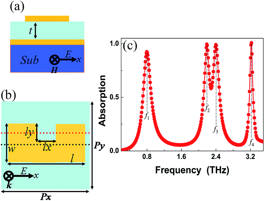 | ||
| Fig. 1 (a) and (b) show the side-view and top view of the design of the quad-band MPA; (c) is the absorption response of the quad-band MPA. | ||
Results and discussion
The absorption response of the quad-band MPA is illustrated in Fig. 1(c). Moreover, four separated frequencies (f1, f2, f3, and f4) can be seen in this figure. For the mode f1, its frequency and absorption rate are 0.80 THz and 92.44%, respectively. For resonance at 2.19 THz (mode f2), it has an absorption of 99.50%. The absorption coefficients of modes f3 at 2.40 THz and f4 at 3.22 THz are respectively 99.05% and 99.99%. These results suggest that we can achieve quad-band nearly perfect absorption by only utilizing one patterned resonator, which is different from previous multimer systems.17–35 In contrast to previous MPAs, the presented device can avoid complex and accurate alignments of multiple patterns with different shapes or sizes. These characteristics are quite useful in the design of innovative multiple-band MPAs.To preliminarily understand the mechanism of the quad-band MPA, we introduced a new MPA that consisted of a rectangle-shape patch structure and a dielectric layer on top of a metallic board. The only difference between the new MPA and the original quad-band MPA is that the new MPA has no air gap. That is to say, the parameters of the new MPA are the same as the original quad-band MPA, except for no air gap. Fig. 2(a) shows the absorption response of the new MPA. Moreover, two resonance modes at the frequencies of 0.83 THz and 2.42 THz are observed for the new MPA. It can be seen from Fig. 2(a) and (b) that the first and third resonance modes of quad-band MPA are very close to that of the modes of the new MPA. The slight frequency deviations should be caused by the introduction of the air gap. In other words, the absorption mechanisms of the modes f1, and f3 of quad-band MPA are consistent with the mechanisms of the dual-band absorption in the new MPA. Compared with the absorption of the new MPA, the quad-band MPA shows two new modes: the f2, and f4. These two new modes should be due to the introduction of the air gap in the patch structure.
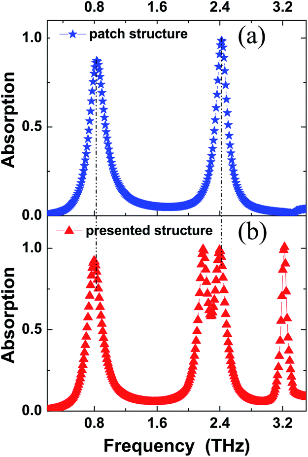 | ||
| Fig. 2 (a) Is the absorption response of the rectangle-shape patch structure (without air gap) of MPA; (b) shows the absorption response of the designed quad-band MPA. | ||
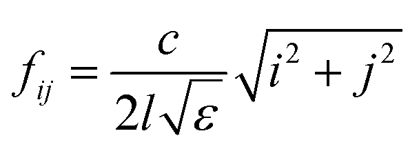
The mechanisms of the new MPA were investigated by analyzing the field distributions (|E| in the center plane of pattern structure, and |Hy| in the plane of y = 0 (the plane of black dot line in Fig. 1(a))) of resonances at 0.83 THz and 2.42 THz, as shown in Fig. 3. It can be seen from Fig. 3(b) and (d) that the |Hy| distributions of the two modes are localized at the dielectric layer of the new MPA. Large enhancement of the |Hy| field in the dielectric layer shows that the |E| distribution of the mode should be distributed at the edges of the resonator. The |E| fields shown in Fig. 3(a) and (c) clearly demonstrate this characteristic. Moreover, only one |Hy| distribution region is found in Fig. 3(b) at a frequency of 0.83 THz. Moreover, three regions can be observed for resonance at 2.42 THz, Fig. 3(d). These properties indicate that the resonances at 0.83 THz and 2.42 THz are the 1-order and 3-order responses of the new MPA, respectively.49,50 Furthermore, the frequencies of the classical metallic patch antenna can be given by51–53
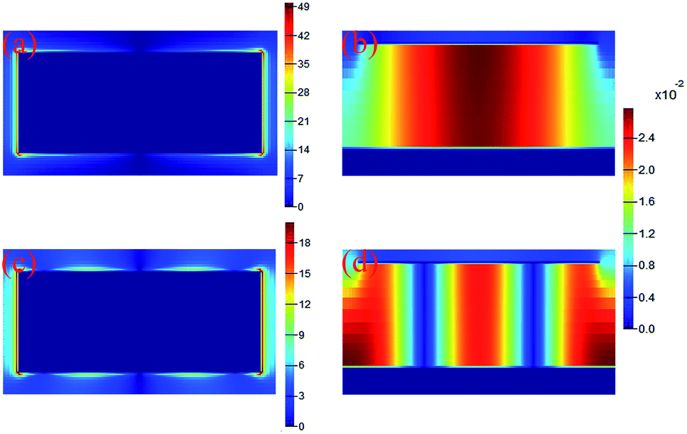 | ||
| Fig. 3 (a) and (b) are the |E| (in the center plane of the pattern structure) and |Hy| (in the plane of y = 0) distributions of new MPA at a frequency of 0.83 THz, respectively; (c) and (d) are the |E| (in the center plane of the pattern structure) and |Hy| (in the plane of y = 0) distributions of new MPA at a frequency of 2.42 THz, respectively. | ||
To reveal the physical mechanism of quad-band MPA, the field distributions (|E| in the center plane of pattern structure, and |Hy| in the plane of y = 0 (the plane of black dot line in Fig. 1(a))) of four different modes are given in Fig. 4. By comparing the field distributions in modes f1 (Fig. 4(a) and (b)) and f2 (Fig. 4(e) and (f)) and the field distributions of two resonance modes in the new MPA in Fig. 3, we can conclude that modes f1 is the 1-order response of quad-band MPA because its field (see Fig. 4(b)) has only a strong resonance region, and mode f3 is attributed to the 3-order response of quad-band MPA because three strong regions can be found in Fig. 4(f). Moreover, for resonance at 2.19 THz, its |E| fields are mainly focused on both edges of the left and right sides of pattern resonator, see Fig. 4(c). Moreover, its |Hy| fields are primarily localized at both sides of the dielectric layer of the quad-band MPA, see Fig. 4(d). Furthermore, we found that the |E| fields and the |Hy| fields are both symmetrically distributed at both sides of the MPA. These field distribution characteristics show that mode f2 is the 1-order response of the left (or right) side of the pattern resonator. In addition, because the length of the left side of the pattern structure is less than that of the total resonator, the frequency of the mode f2 is larger than that of the mode f1. For mode f4, its |E| fields are symmetrically gathered at both edges of the arms of the pattern structure, see Fig. 4(g). Different from the cases of the modes f1, f2, and f3, we observed that there is no |Hy| distributions in the dielectric layer of the MPA when we choose the plane of y = 0 (the plane of black dot line in Fig. 1(a)), see Fig. 4(h). However, the |Hy| fields can be symmetrically distributed at both sides of the dielectric layer of the MPA when the selected plane passes through the arms of the resonator (herein, we chose the plane of y = 6 μm (the plane of the red dot line in Fig. 1(a)) as an example). In other words, the |Hy| fields are symmetrically focused on both sides of the arms of the resonator. As a result, mode f4 should be attributed to the 1-order response of the arms of the pattern structure. Based on the superposition of four separated frequencies of single pattern resonator, quad-band near-perfect MPA was achieved. Compared with the previous design of multiple-band MPAs using the multimer structures, the designed MPA has only one metallic pattern, which imparts the MPA the advantages of a simple and compact unit structure, a novel physical picture. These merits are useful in the design of a new type of multiple-band MPAs.
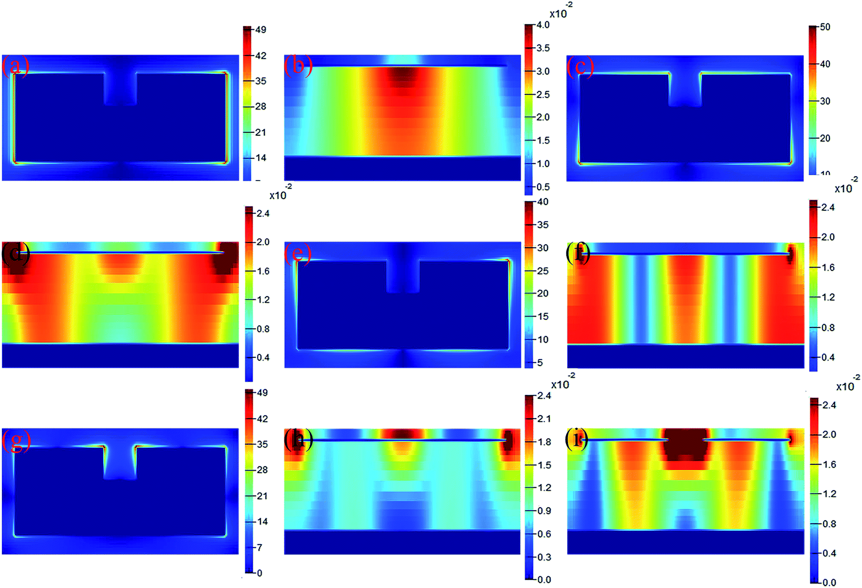 | ||
| Fig. 4 (a) and (b) are the |E| (in the center plane of resonator) and |Hy| (in the plane of y = 0) distributions of quad-band MPA at 0.80 THz, respectively; (c) and (d) are the |E| (in the center plane of resonator) and |Hy| (in the plane of y = 0) distributions of quad-band MPA at 2.19 THz, respectively; (e) and (f) are the |E| (in the center plane of resonator) and |Hy| (in the plane of y = 0) distributions of quad-band MPA at 2.40 THz, respectively; (g) and (h) are the |E| (in the center plane of resonator) and |Hy| (in the plane of y = 0) distributions of quad-band MPA at 3.22 THz, respectively; (i) is the |Hy| (in the plane of y = 6 μm) distribution of quad-band MPA at 3.22 THz. | ||
As discussed above, the appearances of the modes f2 and f4 are mainly due to the introduction of the air gap in the pattern patch structure. In other words, the introduction of the air gap in the pattern patch structure plays an important role in determining the frequencies of the modes f2 and f4. The frequencies of the modes f1 and f3 should be unchanged when the length (l) and width (w) of the patterned structures are fixed. As shown in Fig. 5(a) and (b), we observed that the frequencies of the modes f1 and f3 vary negligibly or shift when the length (lx) and width (ly) of the air gap are changed. The frequencies and absorption rates of modes f2 and f4 have a large dependence on the changes of lx and ly. Furthermore, by comparing the absorption spectra in Fig. 5, we found that the degree of dependence of the frequencies and absorption rates on ly is larger than that of lx.
 | ||
| Fig. 5 Dependence of the absorption spectra on the size changes (length lx (a), width ly (b)) of the air gap of the quad-band MPA. | ||
The number of resonance peaks can be controlled by introducing photosensitive silicon material54 in the gap of the resonator. The top view of the unit cell is shown in Fig. 6(a). As shown, the red region is the photosensitive silicon, and it is fully embedded in the air gap of the resonator. It can be seen from Fig. 6(b) that the absorption rates of the modes f2 and f4 gradually decrease with the increase in silicon conductivity, whereas the absorption rates of the modes f1 and f3 are nearly unchanged.54 Particularly, only two peaks are found when the silicon conductivity is 1 × 10⁶ S m−1. That is to say, we can achieve the tuning of the peaks via varying silicon conductivity. This property has applications in materials detection and multiple-spectral sensing. Additionally, other active materials, such as phase change materials,55–57 can be used to adjust the number of the resonance peaks.
 | ||
| Fig. 6 (a) Is the top-view of the design of the tunable MPA, of which the air gap of the pattern structure is fully embedded by the photosensitive silicon material; (b) is the absorption spectra of the designed tunable MPA at different conductivity of the photosensitive silicon. | ||
Conclusions
In conclusion, single-patterned resonator based quad-band terahertz MPA with nearly perfect absorption was numerically presented. The MPA is composed of a metallic mirror and a rectangle-shape patch with an air gap separated by an insulating dielectric layer. The patterned metallic structure strongly interacts with the incident waves at four separated frequencies, leading to quad-band nearly perfect absorption. The performance of these resonance modes, in particular, the second and fourth modes, can be controlled through changing the sizes of the air gap in the pattern patch structure. In addition to frequency adjustment, the number of resonance peaks can also be adjusted by introducing photosensitive silicon material in the air gap of the pattern structure. The results prove that the number of resonance peaks can be actively tuned by changing the conductivity of the photosensitive silicon. The simple and compact design of the multiple-band PMA is beneficial in many engineering and technical fields.Acknowledgements
This work was supported by the National Natural Science Foundation of China (Grant No. 11647143), the Natural Science Foundation of Jiangsu Province (Grant No. BK20160189), and the Fundamental Research Funds for the Central Universities (Grant No. JUSRP115A13).References
- N. I. Landy, S. Sajuyigbe, J. J. Mock, D. R. Smith and W. J. Padilla, Phys. Rev. Lett., 2008, 100, 207402 CrossRef CAS PubMed.
- H. Tao, N. I. Landy, C. M. Bingham, X. Zhang, R. D. Averitt and W. J. Padilla, Opt. Express, 2008, 16, 7181–7188 CrossRef PubMed.
- G. M. Akselrod, J. Huang, T. B. Hoang, P. T. Bowen, L. Su, D. R. Smith and M. H. Mikkelsen, Adv. Mater., 2015, 27, 8028–8034 CrossRef CAS PubMed.
- L. Cong, S. Tan, R. Yahiaoui, F. Yan, W. Zhang and R. Singh, Appl. Phys. Lett., 2015, 106, 031107 CrossRef.
- L. Huang, G. Li, A. Gurarslan, Y. Yu, R. Kirste, W. Guo, J. Zhao, R. Collazo, Z. Sitar, G. N. Parsons, M. Kudenov and L. Cao, ACS Nano, 2016, 10, 7493–7499 CrossRef CAS PubMed.
- Y. Radi, C. R. Simovski and S. A. Tretyakov, Phys. Rev. Appl., 2015, 3, 037001 CrossRef.
- R. Walter, A. Tittl, A. Berrier, F. Sterl, T. Weiss and H. Giessen, Adv. Opt. Mater., 2015, 3, 398–403 CrossRef CAS.
- V. S. Asadchy, I. A. Faniayeu, Y. Radi, S. A. Khakhomov, I. V. Semchenko and S. A. Tretyakov, Phys. Rev. X, 2015, 5, 031005 Search PubMed.
- Z. Li, S. Butun and K. Aydin, ACS Photonics, 2015, 2, 183–188 CrossRef CAS.
- B. X. Wang, X. Zhai, G. Z. Wang, W. Q. Huang and L. L. Wang, Opt. Mater. Express, 2015, 5, 227–235 CrossRef.
- B. A. Munk, Frequency selective surfaces: theory and design, John Wiley & Sons, New York, 2000 Search PubMed.
- W. W. Salisbury, US Pat., 2599944, 1952.
- H. T. Chen, Opt. Express, 2012, 20, 7165–7172 CrossRef PubMed.
- B. X. Wang, X. Zhai, G. Z. Wang, W. Q. Huang and L. L. Wang, J. Appl. Phys., 2015, 117, 014504 CrossRef.
- X. Liu, K. Bi, B. Li, Q. Zhao and J. Zhou, Opt. Express, 2016, 24, 20454–20460 CrossRef PubMed.
- C. Zou, P. Gutruf, W. Withayachumanakul, L. Zou, M. Bhaskaran, S. Sriram and C. Fumeaux, Opt. Lett., 2016, 41, 3391–3394 CrossRef PubMed.
- A. E. Cetin, S. Korkmaz, H. Durmaz, E. Aslan, S. Kaya, R. Paiella and M. Turkmen, Adv. Opt. Mater., 2016, 4, 1274–1280 CrossRef CAS.
- G. Yao, F. Ling, J. Yue, C. Luo, J. Ji and J. Yao, Opt. Express, 2016, 24, 1518–1527 CrossRef CAS PubMed.
- Y. Zhang, T. Li, Q. Chen, H. Zhang, J. F. Ohara, E. Abele, A. J. Taylor, H. T. Chen and A. K. Azad, Sci. Rep., 2015, 5, 18463 CrossRef CAS PubMed.
- B. X. Wang, IEEE J. Sel. Top. Quantum Electron., 2017, 23, 4700107 Search PubMed.
- X. Shen, Y. Yang, Y. Zang, J. Gu, J. Han, W. Zhang and T. J. Cui, Appl. Phys. Lett., 2012, 101, 154102 CrossRef.
- B. X. Wang, X. Zhai, G. Z. Wang, W. Q. Huang and L. L. Wang, IEEE Photonics J., 2015, 7, 4600108 Search PubMed.
- Y. Ma, Q. Chen, J. Grant, S. C. Saha, A. Khalid and D. R. S. Cumming, Opt. Lett., 2011, 36, 945–947 CrossRef PubMed.
- S. Bhattacharyya, S. Ghosh and K. V. Srivastava, J. Appl. Phys., 2013, 114, 094514 CrossRef.
- B. X. Wang, G. Z. Wang, L. L. Wang and X. Zhai, IEEE Photonics Technol. Lett., 2016, 28, 307–310 CrossRef.
- S. Liu, J. Zhuge, S. Ma, H. Chen, D. Bao, Q. He, L. Zhou and T. J. Cui, J. Appl. Phys., 2015, 118, 245304 CrossRef.
- G. Kajtar, M. Kafesaki, E. N. Economou and C. M. Soukoulis, J. Phys. D: Appl. Phys., 2016, 49, 055104 CrossRef.
- Z. Su, J. Yin and X. Zhao, Opt. Express, 2015, 23, 1679–1690 CrossRef CAS PubMed.
- M. P. Hokmabadi, D. S. Wilbert, P. Kung and S. M. Kim, Phys. Rev. Appl., 2014, 1, 044003 CrossRef.
- S. Li, J. Gao, X. Cao, Z. Zhang, Y. Zheng and C. Zhang, Opt. Express, 2015, 23, 3523–3533 CrossRef CAS PubMed.
- B. X. Wang, G. Z. Wang, T. Sang and L. L. Wang, Sci. Rep., 2016, 7, 41373 CrossRef PubMed.
- J. W. Park, P. V. Tuong, J. Y. Rhee, K. W. Kim, W. H. Jang, E. H. Choi, L. Y. Chen and Y. P. Lee, Opt. Express, 2013, 21, 9691–9702 CrossRef PubMed.
- D. T. Viet, N. T. Hien, P. V. Tuong, N. Q. Minh, P. T. Trang, L. N. Le, Y. P. Lee and V. D. Lam, Opt. Commun., 2014, 322, 209–213 CrossRef CAS.
- B. Zhang, J. Hendrickson and J. Guo, J. Opt. Soc. Am. B, 2013, 30, 656–662 CrossRef CAS.
- A. S. Arezoomand, F. B. Zarrabi, S. Heydari and N. P. Gandji, Opt. Commun., 2015, 352, 121–126 CrossRef CAS.
- F. Ding, Y. Cui, X. Ge, Y. Jin and S. He, Appl. Phys. Lett., 2012, 100, 103506 CrossRef.
- B. X. Wang, L. L. Wang, G. Z. Wang, W. Q. Huang, X. F. Li and X. Zhai, IEEE Photonics Technol. Lett., 2014, 26, 111–114 CrossRef.
- Y. Q. Ye, Y. Jin and S. He, J. Opt. Soc. Am. B, 2010, 27, 498–504 CrossRef CAS.
- B. X. Wang, L. L. Wang, G. Z. Wang, W. Q. Huang, X. F. Li and X. Zhai, J. Lightwave Technol., 2014, 32, 1183–1189 CrossRef.
- S. Liu, H. Chen and T. J. Cui, Appl. Phys. Lett., 2015, 106, 151601 CrossRef.
- B. X. Wang, L. L. Wang, G. Z. Wang, W. Q. Huang, X. F. Li and X. Zhai, J. Lightwave Technol., 2014, 32, 2293–2298 CrossRef.
- X. H. S. Yan, Q. Ma, Q. Zhang, P. Jia, F. Wu and J. Jiang, Opt. Commun., 2015, 340, 44–49 CrossRef.
- X. Yin, C. Long, J. Li, H. Zhu, L. Chen, J. Guan and X. Li, Sci. Rep., 2015, 5, 15367 CrossRef CAS PubMed.
- W. Guo, Y. Liu and T. Han, Opt. Express, 2016, 24, 20586–20592 CrossRef PubMed.
- Y. J. Kim, Y. J. Yoo, K. W. Kim, J. Y. Rhee, Y. H. Kim and Y. P. Lee, Opt. Express, 2015, 23, 3861–3868 CrossRef CAS PubMed.
- C. Cong, M. Zhan, J. Yang, Z. Wang, H. Liu, Y. Zhao and W. Liu, Sci. Rep., 2016, 6, 32466 CrossRef PubMed.
- N. Zhang, P. Zhou, S. Wang, X. Weng, J. Xie and L. Deng, Opt. Commun., 2015, 338, 388–392 CrossRef CAS.
- A. K. Azad, W. J. M. Kort-Kamp, M. Sykora, N. R. Weisse-Bernstein, T. S. Luk, A. J. Taylor, D. A. R. Dalvit and H. T. Chen, Sci. Rep., 2016, 6, 20347 CrossRef CAS PubMed.
- G. Dayal and S. A. Ramakrishna, J. Opt., 2014, 16, 094016 CrossRef.
- G. Dayal and S. A. Ramakrishna, J. Phys. D: Appl. Phys., 2015, 48, 035105 CrossRef.
- A. Sellier, T. V. Teperik and A. D. Lustrac, Opt. Express, 2013, 21, A997–A1006 CrossRef PubMed.
- C. A. Balanis, Antenna theory: analysis and design, Wiley, New York, 1997 Search PubMed.
- X. Y. Peng, B. Wang, S. Lai, D. H. Zhang and J. H. Teng, Opt. Express, 2012, 20, 27756–27765 CrossRef PubMed.
- X. Shen and T. J. Cui, J. Opt., 2012, 14, 114012 CrossRef.
- J. Han, A. Lakhtakia and C. W. Qiu, Opt. Express, 2008, 16, 14390–14396 CrossRef PubMed.
- D. Wang, L. Zhang, Y. Gu, M. Q. Mehmood, Y. Gong, A. Srivastava, L. Jian, T. Venkatesan, C. W. Qiu and M. Hong, Sci. Rep., 2015, 5, 15020 CrossRef CAS PubMed.
- D. Wang, L. Zhang, Y. Gong, L. Jian, T. Venkatesan, C. W. Qiu and M. Hong, IEEE Photonics J., 2016, 8, 5500308 Search PubMed.
| This journal is © The Royal Society of Chemistry 2017 |