 Open Access Article
Creative Commons Attribution 3.0 Unported Licence
MoS2-DNA and MoS2 based sensors
Lirong Yana,
Haixia Shi*b,
Xiaowei Suib,
Zebin Dengc and
Li Gao *c
*c
aDepartment of Gerontology, Affiliated Hospital of Jiangsu University, Zhenjiang 212001, P. R. China
bP. E. Department of Dalian Jiaotong University, Dalian 116028, P. R. China
cInstitute of Life Sciences, Jiangsu University, Zhenjiang 212013, P. R. China. E-mail: gaoli@ujs.edu.cn
First published on 2nd May 2017
Abstract
MoS2, a family member of transition-metal dichalcogenides, has shown highly attractive superiority for detection arising from its unique physical and chemical properties. Coupling MoS2 with DNA recognition events leads to novel sensing platforms. Therefore, it has attracted increasing interest for MoS2 based sensors in the increasing demands of biomedical applications. This has led to its rapid development in field of sensor. This paper summarizes the key issues in the development of MoS2-DNA and MoS2 based sensors related to fluorescence resonance energy transfer (FRET), electrochemical biosensing, and field effect transistors (FET) biosensing for use in the detection of DNA, proteins, metal ions, and others. The detection mechanisms and the advantages of MoS2 are revealed. Future directions in which the field is likely to thrive and some critical challenges are also discussed.
1. Introduction
MoS2 emerging two-dimensional-layered material analogous to graphene has been attracting much attention because of its unique physical and chemical properties, such as extraordinary thermal conductivity, robust mechanical properties, excellent nanoelectronics, unusual optical properties, and energy harvesting properties.1 MoS2 is a family member of transition-metal dichalcogenides. Each Mo is coordinated in a trigonal prismatic geometry to six S atoms; it is constructed by stacking covalently bound S–Mo–S through weak van der Waals interactions,2 which aids in enhancing planar electric transportation properties.3 MoS2 nanosheets are able to adsorb single-stranded DNA by the van der Waals force between nucleobases and the basal plane of MoS2 nanosheets.1 Furthermore, MoS2 nanosheets could be synthesized on a large scale and display strong fluorescence quenching properties in aqueous solution for sensing without further processing comparing with other nanomaterials such as graphene oxide.4 MoS2 shows the similar property and application with graphene oxide.2,5,6 Therefore, MoS2 has been widely applied in sensors that can detect DNA, proteins, metal ions, and other compounds. This paper provides an overview of the current approaches for sensors using DNA as recognition elements and their applications based on MoS2. Future perspectives and some challenges are also discussed.2. Synthesis of MoS2
2.1. Exfoliation
Various methods have been reported about the synthesis of MoS2 nanosheets, including scotch tape based micromechanical exfoliation,7 spontaneous exfoliation,8 chemical exfoliation,9 ultrasound exfoliation,10 liquid exfoliation,11 and electrochemical exfoliation.12 However, scotch tape based micromechanical exfoliation was limited to the fabrication of a small amount of single-layer nanosheet materials with low reproducibility.13 Chemical exfoliation easily results in loss of the pristine semiconducting properties of MoS2 due to structural changes that occur during Li intercalation.9 Ultrasound exfoliation was possible to prepare MoS2 nanosheets maintaining the semiconducting properties comparing with exfoliation using Li intercalation.10 The liquid exfoliation was also easier to transfer the exfoliated products to arbitrary substrates avoiding complex transfer processes. The lateral size in electrochemical exfoliation of MoS2 nanosheets was in the 5–50 μm range, which was much larger than that of chemically or liquid-phase exfoliated MoS2 nanosheets.12 Some improved methods have been reported, for example, the ethanol water mix-solvent sonication combined with grinding14 and high power tip sonication.15 Yao et al. also reported an effective grinding-assisted liquid exfoliation technique to achieve MoS2 nanoflakes. However, this method was not scalable and the size and thickness of exfoliated flakes cannot be controlled.162.2. Chemical vapor deposition (CVD)
Ultrathin MoS2 nanosheets were prepared by using exfoliation methods. With rapid development of study on MoS2, the chemical vapor deposition (CVD) method generating large-area continuous MoS2 films was in great demand. Kong proposed a novel chemical vapor deposition method to synthesize MoS2 films with vertically aligned layers.17 Wu et al. designed MoS2 nanosheets with a high active site density by a microdomain method, and a high edge/basal ratio was obtained.18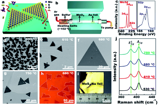 | ||
| Fig. 1 LPCVD synthesis of monolayer MoS2 on Au foils. Reprinted from Shi et al. (2014) with permission from American Chemical Society. | ||
Shi et al. demonstrated, for the first time, the scalable synthesis of monolayer MoS2 on commercially available Au foils via a facile low-pressure CVD/(LPCVD) method (Fig. 1).19 Wang et al. present an approach for synthesizing MoS2 atomic layers with controlled shape and number of layers by the layer-by-layer surface sulfurization of MoO2 microplates. The obtained MoS2 flakes exhibited rhomboidal shape with lengths up to tens of micrometers that was larger than irregular flakes exfoliated from MoS2 crystals.20 It was a challenge to obtain crystalline MoS2 thin film with controlled number of layers by CVD than graphene because no catalyst was involved in the growth of MoS2. CVD has an advantage of growing uniform MoS2 on a large scale. However, it is an expensive method and employs complicated procedures.21 The synthesis of islands on the order of tens of nanometers grown by physical vapor deposition (PVD). It was difficult for achieving coverages in excess of 0.3 ML (monolayer) without compromising the structural quality of the MoS2 that has been reported for the (111) faces of Cu22 and Au.23 Grønborg et al. present a growth method based on reactive PVD that solved this problem and permitted the growth of MoS2 SL (single layer) with an almost unity coverage.24
2.3. Other methods
Various synthetic methods were explored in preparing MoS2 nanomaterials with specific morphologies and unique properties, including gas-phase reactions or solid–gas,25 thermal decomposition,26 laser ablation,27 sonochemical synthesis,28 magnetron sputtering,29 and electron beam irradiation activation.30 However, the morphology and size of the products were hard to control. Compared with the other methods, hydrothermal synthesis was considered as an effective way to prepare inorganic nanomaterials in mild synthetic conditions.31 Many types of MoS2 micro/nano materials with various morphologies were made in the above approaches, such as nanotubes,32 fullerene-like nanoparticles,33,34 nanoplates,35,36 nanorods,37 nanowires,38 nanoflowers,39 and nanospheres,40 nanoribbons,41 nanoboxes42 and hierarchical hollow cubic cages.43 However, it was still a challenge to fabricate some novel structures of MoS2 with the controlled morphologies in mild reaction conditions.44 In addition, the scale up of current processes were limited because of expensive or corrosive precursors.3. Detection using MoS2-DNA based sensors
3.1. Detection based on FRET
MoS2 monolayer shows dramatic improvement in photoluminescence quantum efficiency because of the specific 2D confinement of electron motion and the absence of interlayer perturbation. The improvement of photoluminescence in MoS2 monolayer is also due to the fact that the monolayer, differently from few layer and bulk MoS2, had a direct bandgap.45–47 Compared with other nano-materials, except high fluorescent quenching efficiency, cheap bulk MoS2 materials can be facilely synthesized in large scale and directly dispersed in aqueous solution.1,48 When a ssDNA probe is absorbed on the surface of MoS2, the nucleobases are buried between the densely negatively charged helical phosphate backbones. After combining with its target, this made weakly interact with the MoS2 causing the dye-labeled probe is away from the surface of MoS2.2,49 This results in retention of the fluorescence of the probe. Therefore, MoS2 nanosheets can act as efficient dye quenchers,1,2 which have been employed to develop fluorescent sensing systems using DNA as recognition units (as shown in Table 1).| Detected element | DNA probe | Donor, Exc/Em [nm] | MQE | Detection range or detection linear range | LOD | References |
|---|---|---|---|---|---|---|
| a Exc, excitation; Em, maximum emission wavelength; MQE, maximum quenching efficiency; LOD, limit of detection. | ||||||
| Target DNA | ssDNA | FAM, 494/520 nm | 98% | 0–15 nM | 500 pM | Zhu et al. (2013)2 |
| Target DNA | ssDNA | FAM, 490/520 nm | 95% | 0 to 200 pM | 15 pM | Huang et al. (2015)50 |
| Target DNA | ssDNA | TAMAR, 565/580 nm | 90% | 0 to 50 nM | 0.5 fM | Huang et al. (2015)52 |
| Disease-related genes | Hairpin loop DNA | AgNCs, 563/623 nm | 90% | 10 to 200 nmol | 4.4 nmol | Cao et al. (2015)55 |
| Dam activity | dsDNA | FAM, 495/518 nm | About 90% | 0.2–20 U mL−1 | 0.14 U mL−1 | Deng et al. (2015)51 |
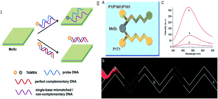
Huang et al. reported a novel MoS2-based fluorescent biosensor for DNA detection via hybridization chain reactions (HCRs). The detection limit in this strategy was 15 pM.50 Including DNA hybridization, Deng et al. described a simple signal-on fluorescence DNA methyltransferase (MTase) activity assay using a MoS2 nanosheet. The Dam MTase activity can be quantified accordingly. Based on this assay, a linear range of 0.2–20 U mL−1 was achieved with high sensitivity and selectivity.51 Huang et al. combined microfluidic biosensor for fluorescent DNA detection based on single-layered MoS2 nanosheets (Fig. 2).52 Yang et al. further present a novel microfluidic biosensor for sensitive fluorescence detection of DNA based on 3D architectural MoS2/multi-walled carbon nanotube (MWCNT) nanocomposites.53 Some label-free detection based on MoS2-DNA sensors were also reported. In these papers, the probes without fluorescence were used and maybe lower the cost for detection. DNA oligonucleotides induced size control of layered MoS2 was considered a label-free bioassay for the detection of single-nucleotide polymorphism.54 Cao et al. developed a simple, low-cost and sensitive DNA sequences detection biosensor based on a label-free molecular beacon (MB) whose DNA hairpin structure terminal had a guanine-rich sequence that can enhance fluorescence of silver nanoclusters (Ag NCs). Even one nucleotide mismatched target can also be distinguished using this sensor.55
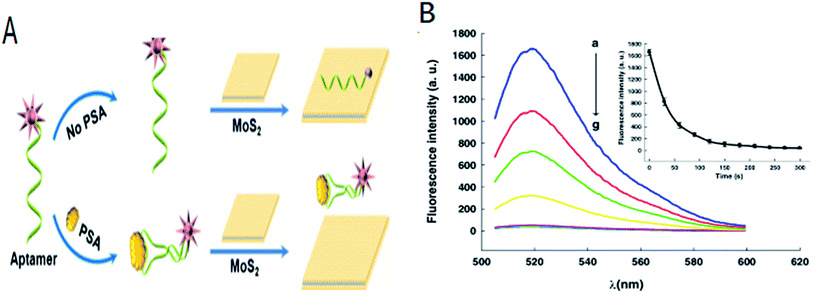
Many biological processes were related with the proteins. MoS2-DNA based sensors were also developed to detect various proteins. Kong et al. proposed a novel aptamer-functionalized MoS2 nanosheet fluorescent biosensor that detected PSA (as shown in Fig. 3). PSA was important for the early diagnosis of prostate cancer. The aptamer probe modified with FAM label at its 5′-terminal was absorbed on the surface of MoS2. The fluorescence of the FAM-labeled aptamer was largely quenched owing to transfer of energy between the dye molecules and the MoS2. In the presence of PSA, the FAM-labeled aptamer adopted a rigid structure owing to binding with the PSA. The affinity of the aptamer with the MoS2 decreased resulting in the release of the aptamer from the MoS2 surface and the fluorescence signal was restored. PSA was detected with a limit of 0.2 ng mL−1.48 Ge et al. developed a novel fluorescence-activated MoS2-DNA nanosheet biosensor for detecting proteins based on the self-assembled architecture of a DNA aptamer and a MoS2 nanosheet.1 In order to improve the sensitivity of detection, Xiang et al. combined the terminal protection of small-molecule-linked DNA and exonuclease III (Exo III)-aided DNA recycling amplification to detect protein based on MoS2 nanosheet. In this method, protein was recycling used and resulted in the improvement of sensitivity for detection comparing with other methods. The detection limit was 0.67 ng mL−1 using the streptavidin (SA)-biotin system as a model.56
Detection of metal ions found in biological systems and in the environment was an attracted intense attention area of research. Mao et al. used for the first time single layer MoS2 as the fluorescence quencher to design a detection method for Ag+ with excellent robustness, selectivity and sensitivity. The detection limit in this assay was 1 nM for Ag+.57 Zhang developed a novel fluorescent biosensor for uranyl ion (UO22+) detection in aqueous environment based on the specific recognition of DNAzyme and MoS2. The detection limit in this assay was 2.14 nM.58
3.2. Detection based on electrochemistry
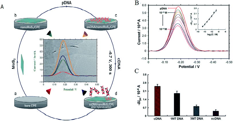
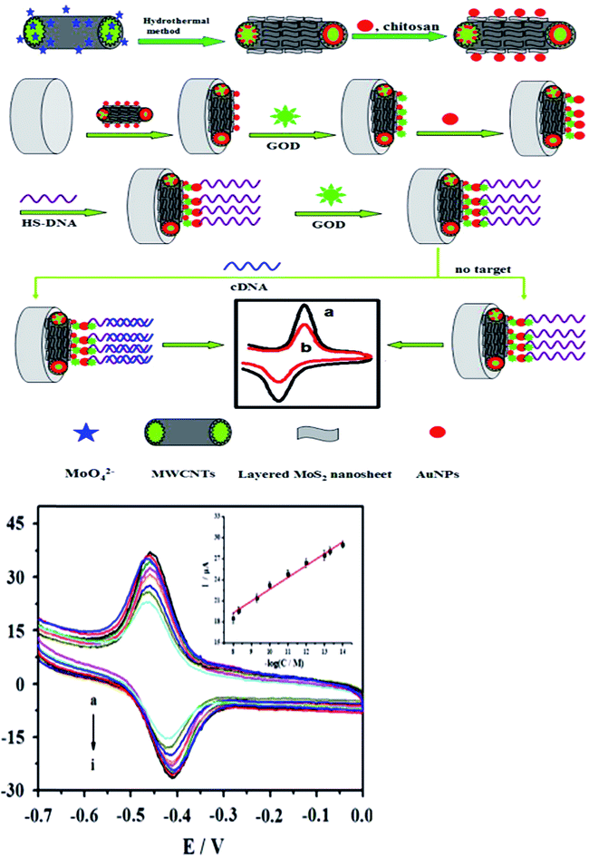
Electrochemistry was an important tool for sensing. MoS2 was quickly used to develop electrochemical DNA-based sensors. Some papers have reported electrochemical DNA-based sensors based on MoS2 possess the exceptional physical and electrochemical properties for detections. Loo et al. reported the principle of detection was based on the differential affinity of molybdenum disulfide nanoflakes towards single-stranded DNA and double-stranded DNA.59 Based on the different affinity toward ssDNA versus dsDNA of the thin-layer MoS2 nanosheets, Wang et al. performed the assay of tlh gene sequence from 1.0 × 10⁻¹⁶ M to 1.0 × 10⁻¹⁰ M with a detection limit of 1.9 × 10⁻¹⁷ M. The detection method described here was without labeling and the use of amplifiers, which resulted in the priority in sensitivity, simplicity, and costs. Furthermore, the proposed sensing platform could be extended to detect more targets (as shown in Fig. 4).60Some functional materials have been decorated on MoS2 to form MoS2-based composite materials in order to further enhance the properties and broaden the applications of MoS2. MoS2-based composite materials have many significant advantages comparing with MoS2. This maximized the advantages and minimized the drawbacks of the individual components. The composites can improve the sensitivity for DNA detection. Huang et al. constructed an ultrasensitive electrochemical DNA biosensor by assembling a thiol-tagged DNA probe on a MoS2/MWCNT and gold nanoparticle (AuNP)-modified electrode coupled with glucose oxidase (GOD). The MoS2/MWCNT composites film possessed large specific surface area and excellent biocompatibility. This increased the immobilization of GOD and enhanced the stability of the DNA probe. Moreover, the GOD membranes as tracer brought about higher current response and higher sensitivity. The detection signals were amplified (as shown in Fig. 5). The detection for DNA was down to 0.79 fM with a linear range from 10 fM to 107 fM. One-base mismatched DNA can be differentiated in this method.3 Chu et al. made nano MoS2/graphene composites by integrating nano MoS2 and graphene through hydrothermal process and ultrasonic method. They developed an electrochemical circulating tumor DNA sensing platform based on this material. The cost and simplicity of the sensor preparation was decreased.61 Including MoS2 and materials (MWCNT and graphene) composites, MoS2 and chemicals, such as polyaniline (PANI) and thionin that have some electrical conductivity, formed the composites improving the electrical property for high sensitivity. Wang et al. prepared a layered MoS2–thionin composite to fabricate a double-stranded DNA (dsDNA) electrochemical biosensor. The linear range over dsDNA concentration from 0.09 ng mL−1 to 1.9 ng mL−1 was obtained. Moreover, single-stranded DNA (ssDNA) can be detected.62 Yang et al. synthesized a PANI–MoS2 nanocomposite based on ANI monomer and MoS2. The PANI–MoS2 nanocomposite with 0.054 g of MoS2 can be considered as the optimal sensing platform for high sensitive DNA detection.63 The sensitivity of detection based on MoS2 and materials composites was higher comparing with MoS2 and chemicals composites from publications. It maybe be electrochemical stability, more excellent electrocatalytic activity, and fast charge transfer rate.
The cooperative effects between MoS2 and metal compounds paved the way to explore a variety of sensing applications. This can not only provide the couple sites with DNA but also improve the sensitivity of detection.64 Proteins were also detected by using MoS2 composites-based sensors. Immunoglobulin E (IgE) was one of important proteins. Shi et al. reported the CdS–MoS2 composites immobilized on glassy carbon electrode surface as ECL emitter attached a complementary ssDNA (NH2-ssDNA) of IgE. IgE aptamer (T-Apt) with DNAzyme-AuNPs hybridized with NH2-ssDNA to form dsDNA. The DNAzyme with horseradish peroxidase-like activity could electrocatalyze the reduction of H2O2. The changed ECL intensity was proportional to concentration of IgE in the range of 0.001–10.0 nM with the detection limit of 0.34 pM (S/N = 3).65 Liu et al. developed a novel competitive electrochemiluminescence (ECL) aptasensor based on CdSe/ZnS quantum dots (QDs) functionalized MoS2 modified electrode for sensitive IgE detection using horseradish peroxidase (HRP) catalyzed biocatalytic precipitation (BCP) for signal quenching. This fabricated aptasensor displays a linear range from 0.5 pM to 0.5 nM with a detection limit of 0.18 pM (S/N = 3).66 Liu et al.'s method had higher sensitivity than Shi et al.'s method. Other proteins were also reported by using MoS2 composites-based sensors. Su et al. developed a MoS2-based electrochemical aptasensor for the simultaneous detection of thrombin based on gold nanoparticles-decorated MoS2 nanocomposites. This aptasensor could simultaneously determine thrombin as low as 0.0012 nM.67 These results showed the signal amplification can be achieved by hybridizing MoS2 with other components due to synergy effect. Therefore, the multifarious sensors have attracted more attention by some researchers as a new era (Table 2).
| Sensor materials | Detected element | Detection range or detection linear range | Detection limit | References |
|---|---|---|---|---|
| CdS–MoS2 nanocomposites | IgE | 0.001–10.0 nM | 0.34 pM | Shi et al. (2015)65 |
| MoS2 | DNA | 1.0 × 10⁻¹⁶ M to 1.0 × 10⁻¹⁰ M | 1.9 × 10⁻¹⁷ M | Wang et al.(2015)60 |
| MoS2–thionin composite | DNA | 0.09 to 1.9 ng mL−1 | 0.17 μA mL ng−1 | Wang et al. (2014)62 |
| RNA | 10 ng mL−1 to 200 ng mL−1 | 0.0022 μA mL ng−1 | ||
| MoS2/MWCNT | DNA | 10 fM to 107 fM | 0.79 fM | Huang et al. (2014)3 |
| CdSe/ZnS quantum dots (QDs)–MoS2 | IgE | 0.5 pM to 0.5 nM | 0.18 pM | Liu et al. (2016)66 |
| AuNPs–MoS2 nanocomposites | ATP | 0.74 nM | Su et al. (2016)67 | |
| Thrombin | 0.0012 nM |
4. Detection based on MoS2 sensors
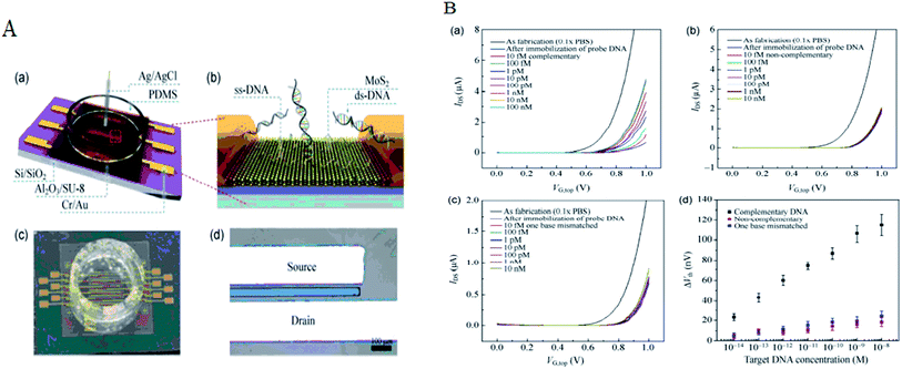
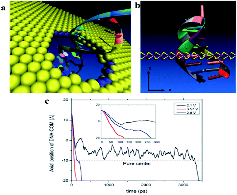
The detection based on MoS2 sensors were mainly using field-effect transistor (FET) that can offer a real-time and efficient sensing platform for a variety of target analytes because of rapid electrical detection without fluorescence-labeling. Highly sensitive and rapid detection of biomolecules with a bioelectronic field-effect transistor was essential for clinical, military, or environmental applications.68,69 FETs with two-dimensional (2D) nanomaterials attracted great attention owing to their many interesting electrical, optical, and mechanical properties.70 MoS2 with the bandgap is different from the pristine graphene. Single layer of MoS2 has a large intrinsic bandgap of 1.8 eV.71 Therefore, MoS2 was applied in FET as a sensor. Lee et al. investigated a field-effect transistor (FET) with few-layer MoS2 as a sensing-channel material for label-free detection of the hybridization of DNA molecules. Hybridization of DNA molecules adsorbed on the MoS2 channel resulted in a shift of the threshold voltage in the negative direction and an increase in the drain current.72 Lee et al. further demonstrated a non-volatile memory field-effect transistor (FET) for hybridization of single-stranded target DNA molecules with single-stranded probe DNA molecules physically adsorbed on the MoS2 channel. This resulted in a shift of the threshold voltage (Vth) in the negative direction and an increase in the drain current because of the change in the surface charge density of the channel. The low detection limit was 10 fM in this method (as shown in Fig. 6).73 Loan et al. first stacked graphene on a CVD MoS2 to perform the differentiation of complementary and one-base mismatched DNA with the graphene/MoS2 heterostructure. The concentration as low as 1 aM (10−18 M) can be detected.70 Metal ion was also reported for detecting by FET. Zhou et al. reported a DNA-functionalized MoS2 nanosheet/gold nanoparticle hybrid FET sensor for the ultrasensitive detection of Hg2+ in an aqueous environment. The sensor shows a rapid response (1–2 s) to Hg2+ and an ultralow detection limit of 0.1 nM.74Some researchers focused on sequencing using MoS2. The strong interaction between graphene and DNA and the high translocation velocity were the challenges for graphene nanopore on DNA sequencing. MoS2 nanopore has shown promising potential for applications of DNA sequencing because MoS2 is highly preferable to graphene in terms of DNA electronic base sensing. MoS2 nanopore showed a distinct ionic current signal for single-nucleobase detection with a SNR of 15 using the simulation. The band gap of MoS2 was significantly changed when bases are placed on the top of pristine MoS2. DNA showed a nonsticky behavior and a more distinguishable signature per base using MoS2 nanopore (as shown in Fig. 7).75 Aluru et al. found that a single-layer MoS2 was an extraordinary material (with a SNR > 15) for DNA sequencing by two competing technologies using atomistic and quantum simulations. A MoS2 nanopore shows four distinct ionic current signals for single-nucleobase detection with low noise.69 This can solve the problem that the noise increased in the detection process because the strong adsorption of DNA on graphene surface in graphene nanopore. Feng et al. further introduced a viscosity gradient system based on room-temperature ionic liquids (RTILs) to control the dynamics of DNA translocation through a nanometer-size pore fabricated in a thin MoS2 membrane solving the high translocation velocity (3000–50![[thin space (1/6-em)]](https://www.rsc.org/images/entities/char_2009.gif) 000 nt per m per s) of DNA molecules moving across such membranes limits their usability. This was the first time to statistically identify the DNA oligomer and the order of current of DNA oligomer was poly(A)30 > poly(T)30 > poly(C)30 > poly(G)30 when DNA oligomer translocates through the MoS2 nanopore.76 In addition, MoS2 nanoribbon was also used for sequencing. Thomas analyzed the transmission of narrow semiconducting nanoribbons designed from MoS2.77 Smolyanitsky et al. proposed an aqueous functionalized molybdenum disulfide nanoribbon suspended over a solid electrode as a capacitive displacement sensor aimed at determining the DNA sequence. The results suggested a realistic, inherently base-specific, high-throughput electronic DNA sequencing device as a cost-effective de novo alternative to the existing methods.78 However, the velocity of DNA passing through the nanopore and nanoribbon was too high in these experiments. It was still a challenge for achieving single-base resolution.
000 nt per m per s) of DNA molecules moving across such membranes limits their usability. This was the first time to statistically identify the DNA oligomer and the order of current of DNA oligomer was poly(A)30 > poly(T)30 > poly(C)30 > poly(G)30 when DNA oligomer translocates through the MoS2 nanopore.76 In addition, MoS2 nanoribbon was also used for sequencing. Thomas analyzed the transmission of narrow semiconducting nanoribbons designed from MoS2.77 Smolyanitsky et al. proposed an aqueous functionalized molybdenum disulfide nanoribbon suspended over a solid electrode as a capacitive displacement sensor aimed at determining the DNA sequence. The results suggested a realistic, inherently base-specific, high-throughput electronic DNA sequencing device as a cost-effective de novo alternative to the existing methods.78 However, the velocity of DNA passing through the nanopore and nanoribbon was too high in these experiments. It was still a challenge for achieving single-base resolution.
5. Conclusions and outlook
This paper provides a short history for MoS2-DNA and MoS2 based sensors. MoS2, as a star among materials and widely studied by researchers worldwide, has drawn considerable interest in many fields. In this review, recent developments in MoS2-DNA and MoS2 based sensors for the detection of DNA, proteins, and heavy metal ions are described and discussed using their unique structure that contribute to their exceptional chemical and physical properties. Those properties lead to a broad range of applications in sensing. Some researchers have reported that MoS2-DNA and MoS2 sensors had relatively high sensitivity when compared with other nanomaterials; for example, the detection limitation based on MoS2-DNA sensors for DNA was 0.5 fM (ref. 52) higher than 0.5 pM based on graphene oxide-DNA sensors.79 MoS2 is also highly preferable to graphene in terms of electronic-based sensing of DNA.75 Therefore, this study helps to provide useful solutions related to some of the world's key problems, such as water and food security and the development of rapid and sensitive medical analysis methods.Currently, the investigation of biosensing applications using MoS2 is still in the early stage.
Some challenges related to sensing based MoS2-DNA and MoS2 remain and need to be resolved. (1) ssDNA is absorbed on the surface of MoS2, and not all dsDNA can detach from the surface of MoS2 after the complementary ssDNA, protein or other molecules combine to ssDNA. This hinders further improvement of the sensitivity of reported DNA sensors. (2) MoS2, as a newly discovered material, faces some challenges including improving synthesis methods and extending its application in various fields. (3) MoS2 properties such as the number of layers, sizes, morphology, functional groups and thickness influence the performance of DNA sensors, especially for electrochemical DNA sensors. (4) The large surface of low density MoS2 in mass production may be difficult to handle, which can lead to health risks caused by inhaling and handling toxic reducing chemicals. (5) MoS2 integrates with micro-fabrication techniques, such as current complementary metal oxide semiconductor (CMOS) technologies, which can increase potential access for the development of label-free, low-cost and high-throughput detection arrays for sensing. However, the stability, selectivity and reproducibility of the devices based on MoS2 should be further improved.
Acknowledgements
This work was supported by Jiangsu University (Grant no. 13JDG005), Natural Science Foundation of Liaoning Province (201601268), the Universities Natural Science Research Project of Jiangsu Province (Grant no. 15KJB180001), a project funded by the Priority Academic Program Development of Jiangsu Higher Education Institutions.References
- J. Ge, E. C. Ou, Q. R. Yu and X. Chu, J. Mater. Chem. B, 2014, 2, 6255 Search PubMed.
- C. F. Zhu, Z. Y. Zeng, H. Li, F. C. Li, H. Fan and H. Zhang, J. Am. Chem. Soc., 2013, 135, 5998 CrossRef CAS PubMed.
- K. J. Huang, Y. J. Liu, H. B. Wang, Y. Y. Wang and Y. M. Liu, Biosens. Bioelectron., 2014, 55, 195 CrossRef CAS PubMed.
- A. Splendiani, L. Sun, Y. B. Zhang, T. S. Li, J. Kim, C. Y. Chim, G. Galli and F. Wang, Nano Lett., 2010, 10, 1271 CrossRef CAS PubMed.
- F. Li, Y. Huang, Q. Yang, Z. T. Zhong, D. Li, L. H. Wang, S. P. Song and C. H. Fan, Nanoscale, 2010, 2, 1021 RSC.
- C. H. Lu, J. Li, J. J. Liu, H. H. Yang, X. Chen and G. N. Chen, Chem.–Eur. J., 2010, 16, 4889 CrossRef CAS PubMed.
- B. Radisavljevic, A. Radenovic, J. Brivio, V. Giacometti and A. Kis, Nat. Nanotechnol., 2011, 6, 147 CrossRef CAS PubMed.
- L. Dong, S. Lin, L. Yang, J. J. Zhang, C. Yang, D. Yang and H. B. Lu, Chem. Commun., 2014, 50, 15936 RSC.
- G. Eda, H. Yamaguchi, D. Voiry, T. Fujita, M. Chen and M. Chhowalla, Nano Lett., 2011, 11, 5111 CrossRef CAS PubMed.
- V. Šteng and J. Henych, Nanoscale, 2013, 5, 3387 RSC.
- K. M. Zhou, N. N. Mao, H. X. Wang, Y. Peng and H. L. Zhang, Angew. Chem., Int. Ed., 2011, 50, 10839 CrossRef CAS PubMed.
- N. A. Liu, P. Kim, J. H. Kim, J. H. Ye, S. Kim and C. J. Lee, ACS Nano, 2014, 8, 6902 CrossRef CAS PubMed.
- Z. Y. Zeng, Z. Y. Yin, X. Huang, H. Li, Q. Y. He, G. Lu, F. Boey and H. Zhang, Angew. Chem., Int. Ed., 2011, 123, 11289 CrossRef.
- Y. G. Yao, L. Tolentino, Z. Z. Yang, X. J. Song, W. Zhang, Y. S. Chen and C. P. Wong, Adv. Funct. Mater., 2013, 23, 3577 CrossRef CAS.
- R. J. Smith, P. J. King, M. Lotya, C. Wirtz, U. Khan, S. De, A. O'Neill, G. S. Duesberg, J. C. Grunlan, G. Moriarty, J. Chen, J. Z. Wang, I. M. Andrew, A. I. Minett, V. Nicolosi and J. N. Coleman, Adv. Mater., 2011, 23, 3944 CrossRef CAS PubMed.
- J. Y. Wu, M. N. Lin, L. D. Wang and T. Zhang, J. Nanomater., 2014, 7, 852735 Search PubMed.
- D. Kong, J. C. Wang, J. Cha, M. Pasta, K. J. Koski, J. Yao and Y. Cui, Nano Lett., 2013, 13, 1341 CrossRef CAS PubMed.
- Z. Z. Wu, B. Z. Fang, Z. P. Wang, C. L. Wang, Z. H. Liu, F. Y. Liu, W. Wang, A. Alfantazi, D. Z. Wang and D. P. Wilkinson, ACS Catal., 2013, 3, 2101 CrossRef CAS.
- J. P. Shi, D. L. Ma, G. F. Han, Y. Zhang, Q. Q. Ji, T. Gao, J. Y. Sun, X. J. Song, C. Li, Y. S. Zhang, X. Y. Lang, Y. F. Zhang and Z. F. Liu, ACS Nano, 2014, 8, 10196 CrossRef CAS PubMed.
- X. S. Wang, H. B. Feng, Y. M. Wu and L. Y. Jiao, J. Am. Chem. Soc., 2013, 135, 5304 CrossRef CAS PubMed.
- J. H. Kim, J. Kim, S. D. Oh, S. Kim and S. H. Choi, J. Korean Phys. Soc., 2015, 66, 1852 CrossRef CAS.
- D. Kim, D. Sun, W. Lu, Z. Cheng, Y. Zhu, D. Le, T. S. Rahman and L. Bartels, Langmuir, 2011, 27, 11650 CrossRef CAS PubMed.
- S. G. Sørensen, H. G. Füchtbauer, A. K. Tuxen, A. S. Walton and J. V. Lauritsen, ACS Nano, 2014, 8, 6788 CrossRef PubMed.
- S. S. Grønborg, S. Ulstrup, M. Bianchi, M. Dendzik, C. E. Sanders, J. V. Lauritsen, P. Hofmann and J. A. Miwa, Langmuir, 2015, 31, 9700 CrossRef PubMed.
- Y. Feldman, E. Wasserman, D. J. Srolovitz and R. Tenne, Science, 1995, 267, 222 CrossRef CAS PubMed.
- C. M. Zelenski and P. K. Dorhout, J. Am. Chem. Soc., 1998, 120, 734 CrossRef CAS.
- J. J. Hu, J. S. Zabinski, J. H. Sanders, J. E. Bultman and A. A. Voevodin, J. Phys. Chem. B, 2006, 110, 8914 CrossRef CAS PubMed.
- N. A. Dhas and K. S. Suslick, J. Am. Chem. Soc., 2005, 127, 2368 CrossRef CAS PubMed.
- K. Ellmer, R. Mientus, S. Seeger and B. V. Wei, Phys. Status Solidi A, 2004, 201, 97 CrossRef.
- M. Chhowalla and G. A. J. Amaratunga, Nature, 2000, 407, 164 CrossRef CAS PubMed.
- W. J. Li, E. Shi and J. M. Ko, J. Cryst. Growth, 2003, 250, 418 CrossRef CAS.
- J. Chen, S. L. Li, Q. Xu and K. Tanaka, Chem. Commun., 2002, 16, 1722 RSC.
- H. Hwang, H. Kim and J. Cho, Nano Lett., 2011, 11, 4826 CrossRef CAS PubMed.
- K. Du, W. Fu, R. Wei, H. Yang, S. Liu, S. Yu and G. Zou, Mater. Lett., 2007, 61, 4887 CrossRef CAS.
- Z. Z. Wu, D. Z. Wang and A. K. Sun, J. Cryst. Growth, 2010, 312, 340 CrossRef CAS.
- Z. Z. Wu, D. Z. Wang, X. Liang and A. K. Sun, J. Cryst. Growth, 2010, 312, 1973 CrossRef CAS.
- M. A. Albiter, R. Huirache-Acuna, F. Paraguay-Delgado, J. L. Rico and G. Alonso-Nunez, Nanotechnology, 2006, 17, 3473 CrossRef CAS PubMed.
- R. H. Wei, H. B. Yang, K. Dua, W. Y. Fu, Y. M. Tian, Q. J. Yu, S. K. Liu, M. H. Li and G. T. Zou, Mater. Chem. Phys., 2008, 108, 188 CrossRef CAS.
- G. G. Tang, J. R. Sun, C. Wei, K. Q. Wu, X. R. Ji, S. S. Liu, H. Tang and C. S. Li, Mater. Lett., 2012, 86, 9 CrossRef CAS.
- L. Ma, L. M. Xu, X. Y. Xu, Y. L. Luo and W. X. Chen, Mater. Lett., 2009, 63, 2022 CrossRef CAS.
- Q. Li, E. C. Walter, W. E. V. D. Veer, B. J. Murray, J. T. Newberg, E. W. Bohannan, J. A. Switzer, J. C. Hemminger and R. M. Penner, J. Phys. Chem. B, 2005, 109, 3169 CrossRef CAS PubMed.
- S. Bastide, D. Dophil, J. P. Borra and C. Levy-Clement, Adv. Mater., 2006, 18, 106 CrossRef CAS.
- L. N. Ye, C. Z. Wu, W. Guo and Y. Xie, Chem. Commun., 2006, 45, 4738 RSC.
- L. Ma, W. X. Chen, H. Li and Z. D. Xu, Mater. Chem. Phys., 2009, 116, 400 CrossRef CAS.
- M. Buscema, M. Barkelid, V. Zwiller, H. S. J. V. D. Zant, G. A. Steele and A. Castellanos-Gomez, Nano Lett., 2013, 13, 358 CrossRef CAS PubMed.
- K. P. Wang, J. Wang, J. T. Fan, M. Lotya, A. O'Neill, D. Fox, Y. Y. Feng, X. Y. Zhang, B. X. Jiang, Q. Z. Zhao, H. Z. Zhang, J. N. Coleman, L. Zhang and W. J. Blau, ACS Nano, 2013, 7, 9260 CrossRef CAS PubMed.
- Q. H. Wang, K. Kalantar-Zadeh, A. Kis, J. N. Coleman and M. S. Strano, Nat. Nanotechnol., 2012, 7, 699 CrossRef CAS PubMed.
- R. M. Kong, L. Ding, Z. J. Wang, J. M. You and F. L. Qu, Anal. Bioanal. Chem., 2015, 407, 369 CrossRef CAS PubMed.
- H. D. Ha, D. J. Han, J. S. Choi, M. T. Park and S. Seo, Small, 2014, 10, 3858 CrossRef CAS PubMed.
- J. H. Huang, L. Ye, X. Gao, H. Li, J. B. Xu and Z. G. Li, J. Mater. Chem. B, 2015, 3, 2395 RSC.
- H. M. Deng, X. J. Yang and Z. Q. Gao, Analyst, 2015, 140, 3210 RSC.
- Y. X. Huang, Y. M. Shi, H. Y. Yang and Y. Ai, Nanoscale, 2015, 7, 2245 RSC.
- D. H. Yang, M. Tayebi, Y. X. Huang, H. Y. Yang and Y. Ai, Sensors, 2016, 16, 1911 CrossRef PubMed.
- B. L. Li, H. L. Zou, L. Lu, Y. Yang, J. L. Lei, H. Q. Luo and N. B. Li, Adv. Funct. Mater., 2015, 25, 3541 CrossRef CAS.
- Q. Cao, Y. Teng, X. Yang, J. Wang and E. Wang, Biosens. Bioelectron., 2015, 74, 318 CrossRef CAS PubMed.
- X. Xiang, J. B. Shi, F. H. Huang, M. M. Zheng, Q. C. Deng and J. Q. Xu, Biosens. Bioelectron., 2015, 74, 227 CrossRef CAS PubMed.
- K. Mao, Z. T. Wu, Y. R. Chen, X. D. Zhou, A. G. Shen and J. M. Hu, Talanta, 2015, 132, 658 CrossRef CAS PubMed.
- H. Y. Zhang, Y. J. Ruan, L. Lin, M. G. Lin, X. X. Zeng, Z. M. Xi and F. F. Fu, Spectrochim. Acta, Part A, 2015, 146, 1 CrossRef CAS PubMed.
- A. H. Loo, A. Bonanni, A. Ambrosi and M. Pumera, Nanoscale, 2014, 6, 11971 RSC.
- X. X. Wang, F. X. Nan, J. L. Zhao, T. Yang, T. Ge and K. Jiao, Biosens. Bioelectron., 2015, 64, 386 CrossRef CAS PubMed.
- Y. L. Chu, B. Cai, Y. Ma, M. G. Zhao, Z. Z. Ye and J. Y. Huang, RSC Adv., 2016, 6, 22673 RSC.
- T. Y. Wang, R. Z. Zhu, J. Q. Zhuo, Z. W. Zhu, Y. H. Shao and M. X. Li, Anal. Chem., 2014, 86, 12064 CrossRef CAS PubMed.
- G. H. Zhou, J. B. Chang, H. H. Pu, K. Y. Shi, S. Mao, X. Y. Sui, R. Ren, S. M. Cui and J. H. Chen, ACS Sens., 2016, 1, 295 CrossRef CAS.
- M. Khan, M. N. Tahir, S. F. Adil, H. U. Khan, M. R. H. Siddiqui, A. A. Al-warthan and W. Tre- mel, J. Mater. Chem., 2015, 3, 18753 RSC.
- G. F. Shi, J. T. Cao, J. J. Zhang, Y. M. Liu, Y. H. Chen and S. W. Ren, Sens. Actuators, B, 2015, 220, 340 CrossRef CAS.
- Y. M. Liu, J. J. Yang, J. T. Cao, J. J. Zhang, Y. H. Chen and S. W. Ren, Sens. Actuators, B, 2016, 232, 538 CrossRef CAS.
- S. Su, H. F. Sun, W. F. Cao, J. Chao, H. Z. Peng, X. L. Zuo, L. H. Yuwen, C. H. Fan and L. H. Wang, ACS Appl. Mater. Interfaces, 2016, 8, 6826 CAS.
- M. S. Makowski and A. Ivanisevic, Small, 2011, 7, 1863 CrossRef CAS PubMed.
- D. Sarkar and K. Banerjee, Appl. Phys. Lett., 2012, 100, 143108 CrossRef.
- P. T. K. Loan, W. J. C. Zhang, T. Lin, K. H. Wei, L. J. Li and C. H. Chen, Adv. Mater., 2014, 26, 4838 CrossRef CAS PubMed.
- K. F. Mak, C. Lee, J. Hone, J. Shan and T. F. Heinz, Phys. Rev. Lett., 2010, 105, 136805 CrossRef PubMed.
- D. W. Lee, J. Lee, Y. Sohn, B. Y. Kim, Y. M. Son, H. Bark, J. Jung, M. Choi, T. H. Kim, C. Lee and N. E. Lee, Nano Res., 2015, 8, 2340 CrossRef CAS.
- J. Lee, S. W. Min, H. S. Lee, Y. Yi and S. Yim, J. Mater. Chem. C, 2014, 2, 5411 RSC.
- T. Yang, L. Meng, H. Y. Chen, S. Z. Luo, W. H. Li and K. Jiao, Adv. Mater. Interfaces, 2016, 3, 1500700 CrossRef.
- A. B. Farimani, K. Min and N. R. Aluru, ACS Nano, 2014, 8, 7914 CrossRef CAS PubMed.
- J. D. Feng, K. Liu, R. D. Bulushev, S. Khlybov, D. Dumcenco, A. Kis and A. Radenovic, Nat. Nanotechnol., 2015, 10, 1070 CrossRef CAS PubMed.
- S. Thomas, A. C. Rajan, M. R. Rezapour and K. S. Kim, J. Phys. Chem. C, 2014, 118, 10855 CAS.
- A. Smolyanitsky, B. I. Yakobson, T. A. Wassenaar, E. Paulechka and K. Kroenlein, ACS Nano, 2016, 10, 9009 CrossRef CAS PubMed.
- L. Peng, Z. Zhu, Y. Chen, D. Han and W. H. Tan, Biosens. Bioelectron., 2012, 35, 475 CrossRef CAS PubMed.
| This journal is © The Royal Society of Chemistry 2017 |

