
 Open Access Article
 This Open Access Article is licensed under a Creative Commons Attribution-Non Commercial 3.0 Unported Licence
In-plane growth of large ultra-thin SnS2 nanosheets by tellurium-assisted chemical vapor deposition†
Zhigang Wang and
Fei Pang *
*
Department of Physics, Beijing Key Laboratory of Optoelectronic Functional Materials & Micro-Nano Devices, Renmin University of China, Beijing 100872, China. E-mail: feipang@live.com; Tel: +86-10-82501783
First published on 2nd June 2017
Abstract
Two-dimensional (2D) SnS2 has attracted significant attention as a potential candidate for modern electronics and optoelectronics. However, the in-plane growth of large ultra-thin SnS2 nanosheets (NSs) still remains a great challenge. In this study, we successfully synthesized in-plane SnS2 NSs with sizes up to 280 μm on SiO2/Si substrates via Te-assisted CVD. On mixing SnO2 and Te, SnO2 reacted with Te to form a Sn–Te eutectic mixture with low melting point, which enhanced the volatilization of the SnO2 precursor. On increasing the substrate temperature from 500 °C to 600 °C, the shape of the SnS2 NSs varied from truncated triangle or hexagonal (HEX) to semi-HEX. High temperature enhanced the migration of the SnS2 adatoms on the substrates and over the edge of the SnS2 NSs; thus, the size of the SnS2 NSs increased with temperature. Further discussion indicates that the truncated triangular shape mainly formed for the substrate breaks the intrinsic sixfold symmetry into three-fold symmetry. The systematic investigation will significantly increase our understanding of the synthesis of 2D materials via Te-assisted CVD.
Introduction
Recently, two-dimensional (2D)-layered chalcogenide materials (LCMs), such as MoS2 and WS2, have drawn significant interest due to their unique structures and remarkable properties, which make them promising materials for applications in nanoelectronics.1–4 SnS2 has a similar layered structure as MoS2, in which the Sn layer is sandwiched between two S layers to form a stable three-layer structure.5 SnS2 nanosheets (NSs) have been widely investigated in the fields of photocatalysis and lithium-ion batteries.6 Furthermore, SnS2 is non-toxic, earth-abundant, and environmentally friendly; thus, it has an evident future advantage in nanoelectronics and optoelectronics.7–9 Moreover, SnS2 possesses a large band gap of ∼2.3 eV.10,11 As is well-known, the large band gap can prominently suppress the source-to-drain tunnelling for short channels, making SnS2 a promising candidate for field effect transistors and photodetectors.12–15 Achievement of the controllable growth of the 2D SnS2 NSs is the first step for device applications. Recently, studies on the diverse synthesis methods, property characterizations, and potential applications of 2D SnS2 NSs have rapidly increased.16–18Chemical vapor deposition (CVD) has been proposed as a successful method to synthesize high-quality single-crystalline LCDs, especially on large 2D materials. Peng et al.19 first fabricated SnS2 NSs by sulfuration of the seeded SnO2 on a SiO2/Si substrate, and the size of the NSs was 20–50 μm. Meng et al.7 certified a screw-dislocation-driven spiral growth process for the synthesis of SnS2 NSs on mica, and the average thickness of the NSs was ∼100 nm and the size was ∼43 μm. Then, He et al.12 successfully synthesized SnS2 NSs of several micrometres on carbon cloth. Recently, Zhai et al.8 have also reported large SnS2 NSs of size up to 150 μm synthesized from SnI2 and S. Yang et al.20 have used S and Sn to produce SnS2 NSs ranging from 40 to 70 μm.
Although significant efforts have been made to prepare 2D SnS2, synthesis of large in-plane ultra-thin SnS2 still faces great challenges. Recent reports have shown that via employing a Sn precursor, such as SnI2 (ref. 8) or Sn20 powder, with low melting point, large SnS2 NSs can be fabricated. However, these SnS2 NSs touched each other to form a compact morphology8 and islands were grown on the surface of the vertical SnS2 NSs.20 Although the in-plane growth of SnS2 can be realized using SnO2 as a precursor,10,19 high melting point of SnO2 (Tmelt = 1350 °C) always leads to low vapour pressure of SnS2 in the growth process. These limitations greatly hinder the preparation of large in-plane SnS2 and thus severely restrict its applications.
Recently, Te-assisted CVD21,22 has been shown to be effective for relaxing the reaction conditions of the synthesis. Motivated by this, we introduced Te in the sulfuration process of SnO2 to improve the vapour pressure of the Sn precursor in our CVD system; this method has the potential to efficiently synthesize large SnS2 NSs. By mixing Te with SnO2 powder as the precursor, we successfully synthesized large-scale high quality 2D SnS2 NSs on SiO2/Si substrates. Our experiments suggest that SnO2 reacted with Te to form a Sn–Te eutectic mixture, such as SnTe, with low melting point, as shown in Fig. S1.† The vapour pressure of Sn was tremendously increased and thus improved its growth efficiency. Furthermore, by controlling the substrate temperature from 500 °C to 600 °C, we found that the shape evolution of the SnS2 NSs varied from truncated triangle or hexagonal (HEX) to semi-HEX. Moreover, the size increased with the substrate temperature. As a result, large ultra-thin in-plane SnS2 NSs with sizes up to 280 μm could be synthesized at 600 °C via Te-assisted atmospheric pressure (AP) CVD.
Experimental
Synthesis of the SnS2 NSs on the SiO2/Si substrate
The synthesis strategy for the preparation of SnS2 NSs is schematically illustrated in Fig. 1a. A horizontal tube furnace with two heating zones was used for the synthesis process. A mixture of SnO2 powder (purity 99.9%, Alfa Aesar) and Te powder (purity 99.9%, Alfa Aesar) with a mass ratio of 2![[thin space (1/6-em)]](https://www.rsc.org/images/entities/char_2009.gif) :5 in an alumina boat was loaded into the heating zone I, and cleaned SiO2/Si substrates were placed downstream in the heating zone II. Thus, we could precisely and separately control the temperature of the precursor and substrate. S powder (purity 99.5%, Alfa Aesar) was loaded into another alumina boat that was placed upstream outside the tube furnace, which was heated using a heating belt. Prior to the growth process, the SiO2/Si substrates (∼1 × 1 cm2) with 300 nm thick SiO2 layer were cleaned by a standard ultrasonic process in acetone, isopropyl alcohol, and deionized water for 30 min in sequence, followed by drying with nitrogen (N2) gas. Then, the tube was pumped down to 1 Pa to remove the air and then flushed with high-purity argon gas (Ar) several times and filled with Ar to achieve the AP. First, the two heating zones were heated to 850 °C (I) and 500–600 °C (II), respectively. Then, the S powder was heated to ∼180 °C, determined using a K type thermocouple. The growth process was then sustained for 20 min using 20 sccm Ar as the carrier gas. Finally, the furnace was naturally cooled down to room temperature.
:5 in an alumina boat was loaded into the heating zone I, and cleaned SiO2/Si substrates were placed downstream in the heating zone II. Thus, we could precisely and separately control the temperature of the precursor and substrate. S powder (purity 99.5%, Alfa Aesar) was loaded into another alumina boat that was placed upstream outside the tube furnace, which was heated using a heating belt. Prior to the growth process, the SiO2/Si substrates (∼1 × 1 cm2) with 300 nm thick SiO2 layer were cleaned by a standard ultrasonic process in acetone, isopropyl alcohol, and deionized water for 30 min in sequence, followed by drying with nitrogen (N2) gas. Then, the tube was pumped down to 1 Pa to remove the air and then flushed with high-purity argon gas (Ar) several times and filled with Ar to achieve the AP. First, the two heating zones were heated to 850 °C (I) and 500–600 °C (II), respectively. Then, the S powder was heated to ∼180 °C, determined using a K type thermocouple. The growth process was then sustained for 20 min using 20 sccm Ar as the carrier gas. Finally, the furnace was naturally cooled down to room temperature.
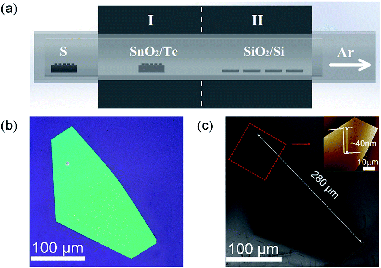 | ||
| Fig. 1 (a) A schematic of the experimental setup, (b) the OM image of the as-grown SnS2 NS at ∼600 °C, and (c) the corresponding SEM image of the SnS2 NSs; the upper-right corner: AFM image of red dashed box of SnS2 NSs. | ||
Characterization
The fundamental structural and componential properties were comprehensively investigated using optical microscopy (OM, Nikon), scanning electron microscopy (SEM, FEI NANOSEM 450), energy dispersive X-ray spectroscopy (EDX, Oxford Instrument) attached to SEM, atomic force microscopy (AFM, Bruker Dimension Icon) and Raman spectroscopy (Renishaw inVia). Photoluminescence (PL) spectroscopy (Horiba Jobin Yvon, LabRAM Aramis) was performed using a laser excitation of 325 nm. The morphologies of SnS2 were characterized using OM, SEM, and AFM. The thickness of the as-grown samples was obtained using AFM. Raman spectroscopy was conducted using a laser excitation of 488 nm. EDX was used to characterize the composition of the products.Results and discussion
After the reaction, the SnS2 NSs were formed on the substrates. Fig. 1b and c show the typical OM and SEM images of the final SnS2 NS on the SiO2/Si substrate grown at 600 °C in the heating zone II. The sizes of the ultra-thin SnS2 NS were up to 280 μm and the thickness was about 40 nm, as measured using AFM and shown in the upper-right corner of Fig. 1c. Peng et al.19 obtained 50 μm SnS2 NSs using SnO2 as the Sn precursor. The results show that the high growth efficiency of SnS2 NSs was manifested by Te-assisted CVD. To clarify the role of Te during the growth process of the SnS2 NSs, we performed two independent experiments. First, we vaporized SnO2 at 850 °C in the heating zone I without Te or S. After being carried by 20 sccm Ar for about 20 min, the weight of SnO2 barely changed. Moreover, no obvious structures were found on the substrate loaded into the heating zone II whose temperature was kept at 600 °C. Second, a mixture of SnO2 and Te was vaporized under the same growth conditions, and the SnTe nanoblocks were obtained on the substrates at 600 °C. The SEM image of SnTe and its corresponding EDX data are shown in Fig. S2.† These two independent experiments suggest a possible growth mechanism: Te melts at a relatively low temperature in the mixture of Te and SnO2 powders, and a small fraction of SnO2 powders dissolves in Te to form a Sn–Te eutectic mixture, such as SnTe, with low melting temperature. Therefore, the amount of the Sn precursor was enhanced via the Te-assisted CVD process, which was similar to that obtained after employing the SnI2 powder as the Sn precursor.8 In a sulfur-rich environment, Te (originating from the reaction SnTe + 2S(gas) = SnS2 + Te(gas)) leaves the reaction product and is carried away by the Ar flow to the downstream. Thus, the growth efficiency of the SnS2 NSs was attributed to the low melting point of the Sn–Te eutectic mixture via the addition of Te to the SnO2 powder, which enhanced the vapour pressure of the Sn precursors in the CVD system.It is generally believed that the effect of the substrate temperature is a key issue for the synthetic control of the 2D LCM. To illustrate the effect of substrate temperature on the growth of the SnS2 NSs, we further adjusted the substrate temperature and investigated the morphology of the SnS2 NSs at various temperatures. Fig. 2 shows the SEM images of the SnS2 NSs grown between 500 °C and 600 °C. Fig. 2d–f show the enlarged SEM images of the SnS2 NSs indicated by the red circle in Fig. 2a–c. In our experiments, mostly large flat semi-HEX-shaped SnS2 NSs were obtained at ∼600 °C, as shown in Fig. 2c. From the SEM images shown in Fig. 2d–f, we found that the shape of the SnS2 NS showed obvious variation from truncated triangular or HEX to semi-HEX, and the size of the SnS2 NSs increased from 3 μm to 280 μm. Thus, the dominating shape of the NSs could be controlled by adjusting the temperature, and the size of the SnS2 NSs increased with temperature from several micrometres to hundreds of micrometres.
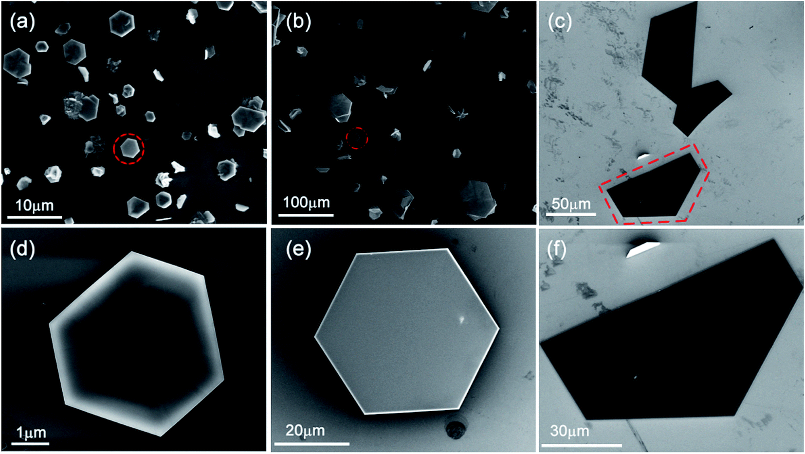 | ||
| Fig. 2 SEM images of the various shapes of SnS2 NSs grown at different temperatures: (a) 500 °C, (b) 550 °C, and (c) 600 °C. The corresponding enlarged SEM images at specified temperature are indicated by the red box (d, e, and f). | ||
To confirm the crystallinity and composition of the NSs investigated via SEM, as shown in Fig. 2, we further used Raman spectroscopy and EDX to characterize them. Accordingly, Fig. 3 shows the Raman and EDX spectroscopy spectra of the corresponding SnS2 NSs shown in Fig. 2d–f. For the SnS2 crystals, two characteristic Raman peaks were assigned as the Eg (∼205 cm−1) mode and the A1g mode (∼313 cm−1). As can be seen from Fig. 3a, the truncated triangular SnS2 NS gown at 500 °C display two main peaks at ∼205 cm−1 and ∼313 cm−1, which correspond to the Eg and A1g phonon modes of SnS2, respectively. On increasing the temperature to 550 °C, the Eg peak at ∼205 cm−1 becomes weaker and still appears in the magnification spectrum, as shown in Fig. 3b. Furthermore, as shown in Fig. 3c, the intense Raman peak of the semi-HEX SnS2 at 313.4 cm−1 was assigned to the A1g mode, and no Eg mode could be found, even in the magnified image. This has been demonstrated in a number of studies8,10,11 that the Eg peak disappears due to reduction in the number of scattering centers available for in-plane scattering when the thickness of the SnS2 NSs is decreased down to the nanometre scale. Raman spectroscopy could confirm that these semi-HEX SnS2 NSs were indeed ultra-thin crystals. During the process of obtaining the Raman spectra, as shown in Fig. 3a–c, we did not observe the Raman peaks at 474, 632, or 774 cm−1 associated with SnO2.20 This implies the complete reaction of the SnO2 and S powders, and the negligible chemical reaction between SnS2 and the SiO2 substrate. The Eg peak vanished in the Raman spectrum of the semi-HEX SnS2 NSs, which demonstrated that ultra-thin SnS2 NSs were obtained at 600 °C.
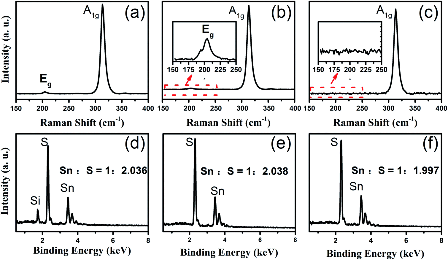 | ||
| Fig. 3 The Raman and EDX spectroscopy spectra of various shapes of SnS2 NSs. (a, b, and c) The Raman spectrum of truncated triangular, HEX, and semi-HEX NSs in (Fig. 2d–f); (d, e, and f) the corresponding EDX spectra. | ||
Furthermore, EDX spectroscopy was employed to explore the composition of the truncated triangular shape SnS2 NSs, as shown in Fig. 3d. The Sn:S atomic ratio of the NSs was 1:2.026, which was very close to 1:2. The HEX and semi-HEX NSs were characterized in the same way. As is evident from their respective EDX spectra displayed in Fig. 3e and f, the atomic ratios close to 1:2 agree well with their expected stoichiometric composition. Moreover, in the EDX spectra without the Te signal, it was observed that the addition of Te did not leave any detectable residues in the grown SnS2 samples.
From the abovementioned discussion, it was concluded that the size of SnS2 increased with the substrate temperature. It is of great value to understand the evolution mechanism of the SnS2 NSs with temperature, which may help to controllably synthesize 2D LCMs in the future. As schematically described in Fig. 4a, the growth reaction actually includes three processes: (1) the diffusion of SnS2 vapor adsorbed onto the substrate, (2) the migration of the SnS2 adatoms, and (3) the desorption of excess adsorbed SnS2. Herein, we divided the migration of the SnS2 adatoms into three cases: M1 was the migration on the substrate surface, M2 was the migration on the surface of the SnS2 NSs, and M3 was the migration over the step edge of the SnS2 NSs. Based on abovementioned discussion, it can be concluded that introduction of Te powder into the SnO2 powder can greatly lower the original melting point of SnO2, allowing a large amount of Sn precursor to volatilize, and the diffusion of the SnS2 vapor adsorbed onto the substrates increases. As a result, we could obtain large SnS2 NSs and the diffusion flux of SnS2 was enhanced. If the supply flux of SnS2 adatoms remains unchanged, the lower temperature of the substrate limits the desorption process of excess adsorbed SnS2, and more nucleation SnS2 sites are formed. Upon increasing the substrate temperature, the desorption of excess adsorbed SnS2 became active, and then, the small SnS2 flakes were easy to vaporize from the substrate and diffusion was enhanced. The decrease in the NSs density with temperature can be related with the number of nucleation sites. A very obvious tendency could be found in which the NSs size increased with the decrease in the NS density from 500 °C to 600 °C, as shown in Fig. 2a–c.
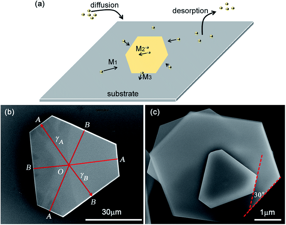 | ||
| Fig. 4 (a) A schematic of the dynamics behaviour in the growth process, M1: migration on the substrates surface, M2: the migration on the surface of the SnS2 NSs, and M3: the migration over the step of the SnS2 NSs. (b) The SEM image of the as-grown truncated triangle SnS2 NSs grown at 550 °C. (c) The SEM image of the overlapped SnS2 crystal grown at 500 °C. | ||
The desorption of excess adsorbed SnS2 with temperature decreased the density of the SnS2 NSs. The migration of the adatoms is another important process in the growth reaction. The temperature-dependent migration coefficient D of the adatoms on the substrate surface is shown in eqn (1), and D has been considered to be related to the migration barrier energy Em via
| D ∝ e−Em/kT | (1) |
Because the Em may linearly increase with the number of dangling bonds,22 we provided a qualitative comparison between the migration energies of the three types of migration. The atoms at a step edge have fewer nearest neighbours; hence, these atoms have more dangling bonds. If the adatoms on the SnS2 surface transfer from the upper layer to the lower layer or substrate over the step edge, there will be a high step-edge barrier.20 When an adatom adsorbs on the surface of the NSs and moves towards a step edge, this potential barrier will hinder the migration over the step edge of the SnS2 NSs and repel the adatom diffusion away from the step edge. Eventually, a new layer grows larger on the former layer and the thickness of the NSs increases. More and more adatoms adsorb on the NS surface, and as a result, the new layer grows up to the same size as the next layer. Thus, the SnS2 NSs grow in a layer-by-layer mode. Higher temperature increases the migration over the step edge of the SnS2 NSs, and more adatoms on the NS surface will skip over the step edge to the substrates; therefore, the size of the NSs increases.
Based on the abovementioned discussion, we could suggest that the temperature increases the migrations of the SnS2 adatoms such as the migrations on the substrate and over the step edge of the NSs. As a result, the size of the SnS2 NSs increases with the substrate temperature. When the growth temperature was gradually increased, the adatoms diffusion increased. Thus, non-equilibrium shaped NSs may be formed at different growth temperatures. The size of the as-grown NSs would augment with an increase in the growth temperature.
In the low-temperature regimes (500 °C and 550 °C), the shape of the SnS2 NSs holds six step edges and an angle between any two adjacent step edges of ∼120°, as shown in Fig. 2d and (e). There are a number of mechanisms that illustrate the formation of NSs: growth temperature,24 step edge barrier,20 and substrate.25 In the case of SnSe2,24 high temperature enhanced the vapour pressure of Se, and then, the amount of Se decreased with temperature; thus, the shape transformed from truncated triangular to HEX. However, at higher temperature (550 °C), we also found HEX shape SnS2 NSs (Fig. 2e) and truncated triangular shape SnS2 with different lengths, as shown in Fig. 4b. Thus, the effect of temperature on the amount of S vapour could be ignored for the low melting temperature of the S powder and both shapes appeared at the same temperature.
The inequality in the edge lengths of the islands on SnS2 (ref. 20) was found in the cooling process and could be explained by the step edge barrier. A normal γ-plot was used to quantify the ratio of the step edge energies such as those of the SnS2 islands.20 Following a similar way, a line was drawn from the centre of an SnS2 NS and perpendicular to a short step edge A (or long step edge, B), as shown in Fig. 4b. The ratios of γB/γA, as shown in Fig. 4b, were 0.76, 0.73, and 0.78. In the same way, we calculated the ratios of γB/γA, as shown in Fig. 2a, to be 0.82, 0.83, and 0.87. Only some of the ratios are close to the ratio of 0.88–0.93 observed in the SnS2 islands.20 Moreover, stacking of the NSs with different angles was observed in our samples at 500 °C, which was also observed in the SnSe2 crystals synthesized via a spiral growth mode in the CVD process (Fig. 4c).25 This implies the step edge barrier that prevents the adatoms on the upper smaller NSs from reaching the lower larger NSs. This is consistent with the observation that the migration over the step edge of the SnS2 NSs is limited at lower temperature. As shown in Fig. 4c, the smaller crystals tend to form truncated triangular crystals, whereas SnSe2 prefer triangular crystals.25 The ratios of γB/γA for the smaller crystals, as shown in Fig. 4c, are 0.7, 0.73, and 0.74.
By calculating the ratios of γB/γA for different truncated triangular shape SnS2 NSs, we found that these ratios were different from 0.7–0.87, which were different from those reported in the previous studies.20 However, it was confirmed that the longer step edge B had a slower growth rate. According to the kinetic Wulff criterion, any growing crystals tend to have the slowest growth faces.26 It has been established that Mo zigzag edges and S zigzag edges are the most energetically favoured edge structures in MoS2,27 which constructs a hexagonal shape with six edges. In the presence of a substrate, the two sides of the SnSe2 zigzag edges are no longer identical.25 The potential breaking of symmetry can be achieved via changing either the edge energy or chemical reaction rate. As is known, SnS2 has a structure similar to that of MoS2 and SnSe2. It should follow a similar principle that an HEX SnS2 NS has six identical edges and these edges can be either Sn zigzag (Sn-zz) edges or S zigzag (S-zz) edges. They attributed this to a difference in the step edge energies.20 As the edges have the same growth rates of the Sn-zz and Sn-zz edges, they tend to form HEX shapes under equilibrium conditions, as shown in Fig. 2e. The unequal step edge lengths imply that the six edges have unequal growth rates to form the truncated triangle shape. From the abovementioned discussion, we found that the temperature and step energy ratio were not the key issue to form truncated triangle SnS2. The substrate that breaks the intrinsic six-fold symmetry into three-fold symmetry manifests truncated triangular SnS2 for the chemical reaction.
AFM was utilized to identify the thickness of the as-grown SnS2 NSs at 600 °C. The AFM images, as displayed in Fig. 5a and b, elucidate that the thickness of the as-grown SnS2 NSs was ∼7.9 nm and ∼12.7 nm, respectively. Each layer of SnS2 comprised three atomic planes covalently bonded in the sequence of S–Sn–S, and the layer interactions depended on the weak van der Waals forces. Taking a theoretic monolayer thickness of ∼0.6 nm into consideration, the thickness of the NSs was ∼13, and ∼21 layers. According to the AFM images, the average roughness of the SnS2 surface was about 0.3 nm, which implied the high crystallinity of the products. Therefore, we fabricated ultra-thin and high crystallinity SnS2 NSs, which have immense applications in electronic and optoelectronic devices.
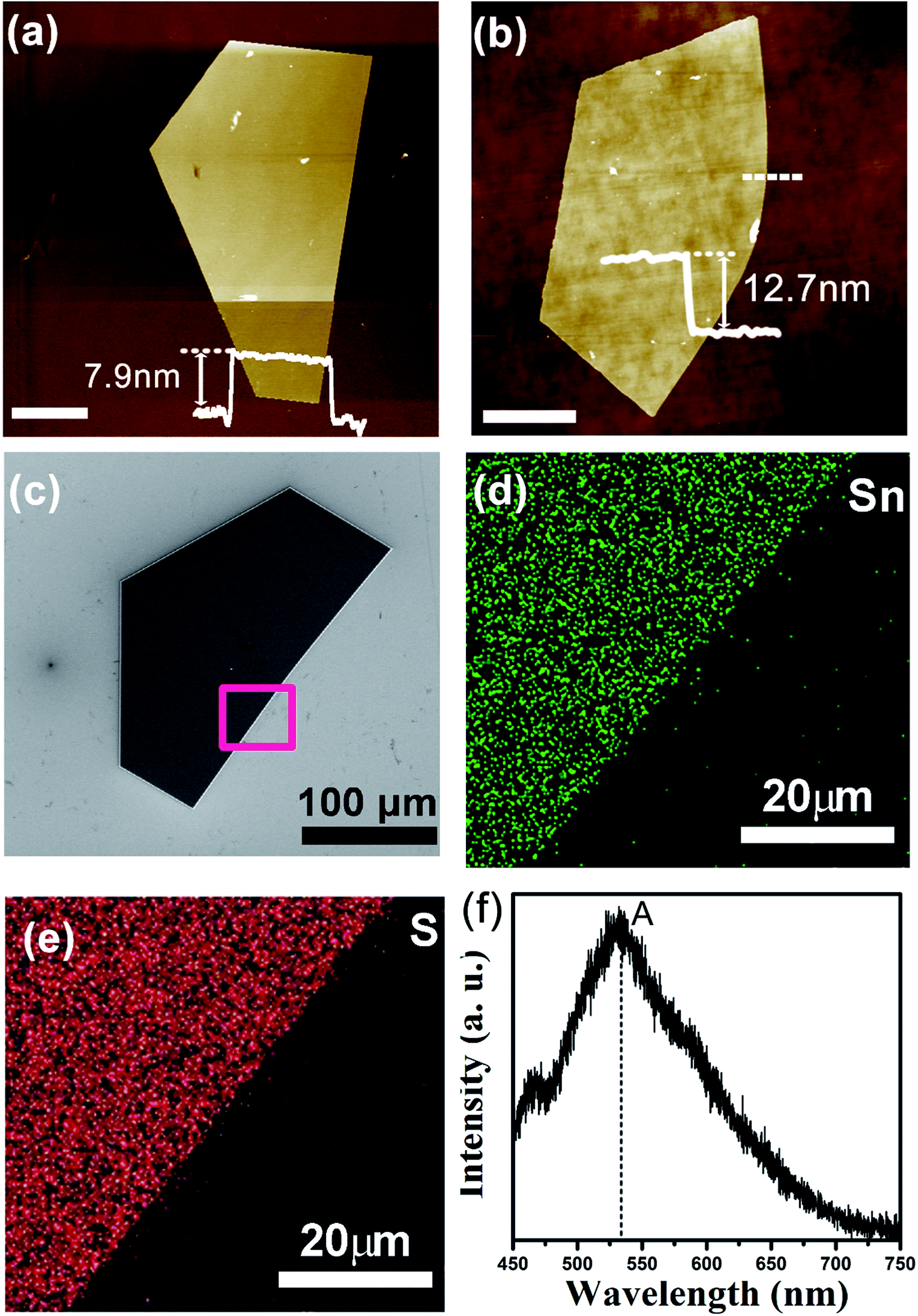 | ||
| Fig. 5 (a and b) The AFM images of the synthesized SnS2 NSs; scale bar: 5 μm. (c) The SEM image of an ultra-thin SnS2 NSs. (d and e) The Sn and S element mapping in the red rectangle region of the NSs. (f) The PL spectroscopy of the SnS2 NSs measured at atmospheric pressure. | ||
To further elucidate the elemental distribution of the sample, we presented the EDX mapping and PL spectroscopy spectra of the SnS2 NSs grown at 600 °C, as shown in Fig. 5c. The signals of the Sn and S elements almost originate from our sample, and a uniform distribution of Sn and S elements was revealed in the selected area, as shown in Fig. 5d–f. Fig. 5f shows the PL spectrum obtained from the SnS2 crystals, and a prominent peak at ∼533 nm was observed. The band gap calculated from the PL spectrum is 2.33 eV, which is similar to that previously reported.28 The measured PL peak at ∼533 nm was generated due to the recombination of electron–hole pairs, which was demonstrated in a number of studies, such as SnS2 nanoparticles made using wet chemistry methods that showed a PL peak at 550 nm,29 the PL peak of the SnS2 NSs appeared between 540 and 562 nm,30 mechanically exfoliated SnS2 flakes presented a band gap of ∼2.23 eV,12 and SnS2 nanocrystals made from chemical vapor transport displayed a band gap of ∼2.25 eV.31 There is a relatively lower or even negligible peak at ∼467 nm. We could not provide a clear explanation for this PL peak. According to a previous study,32 we speculated that it may be due to the radiative recombination of the excitonic absorption generated electrons, which were located at the higher excited energy levels. Herein, we found that the PL intensity was extremely weak due to the indirect band gap of SnS2, which was confirmed by the results found for SnS2 synthesized by other group.28 All these characterizations demonstrate that the sample is a high-quality single-crystalline SnS2 material.
Conclusions
In summary, we presented an effective CVD growth technique to fabricate large ultra-thin SnS2 NSs on SiO2/Si substrates using Te assistance. The high temperature and Te-assistance increases the evaporation pressure of SnS2, and as a result, we could obtain large in-plane SnS2 NSs. Upon increasing the temperature of the substrate, the shape of the SnS2 NSs changes from truncated triangle or HEX to semi-HEX. Further discussion showed that the truncated triangular shape resulted from the substrate that broke the intrinsic six-fold symmetry into three-fold symmetry. Among all the growth temperatures studied herein, large high-crystalline SnS2 NSs with sizes up to 280 μm were obtained on the SiO2/Si substrates at ∼600 °C. The SnS2 NSs are indirect band gap (∼2.23 eV) semiconductors and can be thinned to 7.9 nm. The results show that the Te-assisted CVD process is a powerful tool to design and synthesize other 2D LCMs. A fundamental understanding of the effect of temperature can pave the way towards the controllable growth of the 2D LCMs.Acknowledgements
This work was supported by the Fundamental Research Funds for the Central Universities and the Research Funds of Renmin University of China under Grant No. 14XNLQ07.Notes and references
- Q. H. Wang, K. Kalantar-Zadeh, A. Kis, J. N. Coleman and M. S. Strano, Nat. Nanotechnol., 2012, 7, 699–712 CrossRef CAS PubMed.
- K. F. Mak, K. He, J. Shan and T. F. Heinz, Nat. Nanotechnol., 2012, 7, 494–498 CrossRef CAS PubMed.
- X. Xu, W. Yao, D. Xiao and T. F. Heinz, Nat. Phys., 2014, 10, 343–350 CrossRef CAS.
- D. Voiry, M. Salehi, R. Silva, T. Fujita, M. Chen, T. Asefa, V. B. Shenoy, G. Eda and M. Chhowalla, Nano Lett., 2013, 13, 6222–6227 CrossRef CAS PubMed.
- (a) B. Radisavljevic, A. Radenovic, J. Brivio, V. Giacometti and A. Kis, Nat. Nanotechnol., 2011, 6, 147–150 CrossRef CAS PubMed; (b) C. Ataca, H. Sahin and S. Ciraci, J. Phys. Chem. C, 2012, 116, 8983–8999 CrossRef CAS.
- (a) Z. Zhang, J. Huang, M. Zhang, Q. Yuan and B. Dong, Appl. Catal., B, 2015, 163, 298–305 CrossRef CAS; (b) Z. Zhang, C. Shao, X. Li, Y. Sun, M. Zhang, J. Mu, P. Zhang, Z. Guo and Y. Liu, Nanoscale, 2013, 5, 606–618 RSC; (c) J. Seo, J. Jang, S. Park, C. Kim, B. Park and J. Cheon, Adv. Mater., 2008, 20, 4269–4273 CrossRef CAS.
- J. Xia, D. Zhu, L. Wang, B. Huang, X. Huang and X. M. Meng, Adv. Funct. Mater., 2015, 25, 4255–4261 CrossRef CAS.
- X. Zhou, Q. Zhang, L. Gan, H. Li and T. Zhai, Adv. Funct. Mater., 2016, 26, 4405–4413 CrossRef CAS.
- D. Yang, B. Li, C. Hu, H. Deng, D. Dong, X. Yang, K. Qiao, S. Yuan and H. Song, Adv. Opt. Mater., 2016, 4, 419–426 CrossRef CAS.
- J. H. Ahn, M. J. Lee, H. Heo, J. H. Sung, K. Kim, H. Hwang and M. H. Jo, Nano Lett., 2015, 15, 3703–3708 CrossRef CAS PubMed.
- Y. Huang, E. Sutter, J. T. Sadowski, M. Cotlet, O. L. Monti, D. A. Racke, M. R. Neupane, D. Wickramaratne, R. K. Lake, B. A. Parkinson and P. Sutter, ACS Nano, 2014, 8, 10743–10755 CrossRef CAS PubMed.
- Y. Huang, H. X. Deng, K. Xu, Z. X. Wang, Q. S. Wang, F. M. Wang, F. Wang, X. Y. Li, J. W. Luo and J. He, Nanoscale, 2015, 7, 14093–14099 RSC.
- D. De, J. Manongdo, S. See, V. Zhang, A. Guloy and H. Peng, Nanotechnology, 2013, 24, 025202–025208 CrossRef PubMed.
- H. S. Song, S. L. Li, L. Gao, Y. Xu, K. Ueno, J. Tang, Y. B. Cheng and K. Tsukagoshi, Nanoscale, 2013, 5, 9666–9670 RSC.
- Y. Tao, X. Wu, W. Wang and J. Wang, J. Mater. Chem. C, 2015, 3, 1347–1353 RSC.
- S. Najmaei, Z. Liu, W. Zhou, X. Zou, G. Shi, S. Lei, B. I. Yakobson, J. C. Idrobo, P. M. Ajayan and J. Lou, Nat. Mater., 2013, 12, 754–759 CrossRef CAS PubMed.
- Y. Gong, G. Ye, S. Lei, G. Shi, Y. Ye, J. Lin, X. Zhang, R. Vajtai, S. T. Pantelides, W. Zhou, B. Li and P. M. Ajayan, Adv. Funct. Mater., 2016, 26, 2009–2015 CrossRef CAS.
- C. Y. Su, A. Y. Wu, Y. T. Li, K. K. Liu, W. Zhang, S. Y. Lin, Z. Y. Juang, Y. L. Zhong, F. R. Chen and L. J. Li, Nano Lett., 2011, 11, 3612–3616 CrossRef CAS PubMed.
- G. Su, V. G. Hadjiev, P. E. Loya, J. Zhang, S. Lei, S. Maharjan, P. Dong, P. M. Ajayan, J. Lou and H. Peng, Nano Lett., 2015, 15, 506–513 CrossRef CAS PubMed.
- Y. B. Yang, J. K. Dash, A. J. Littlejohn, Y. Xiang, Y. Wang, J. Shi, L. H. Zhang, K. Kisslinger, T. M. Lu and G. C. Wang, Cryst. Growth Des., 2016, 16, 961–973 CAS.
- Y. Gong, Z. Lin, G. Ye, G. Shi, S. Feng, Y. Lei, A. L. Elías, N. Perea-Lopez, R. Vajtai, H. Terrones, Z. Liu, M. Terrones and P. M. Ajayan, ACS Nano, 2015, 9, 11658–11666 CrossRef CAS PubMed.
- F. Cui, C. Wang, X. Li, G. Wang, K. Liu, Z. Yang, Q. Feng, X. Liang, Z. Zhang, S. Liu, Z. Lei, Z. Liu, H. Xu and J. Zhang, Adv. Mater., 2016, 28, 5019–5024 CrossRef CAS PubMed.
- L. Huang, Y. Yu, C. Li and L. Cao, J. Phys. Chem. C, 2013, 117, 6469–6475 CAS.
- Y. Huang, K. Xu, Z. Wang, T. A. Shifa, Q. Wang, F. Wang, C. Jiang and J. He, Nanoscale, 2015, 7, 17375–17380 RSC.
- J. Wu, Z. Hu, Z. Jin, S. Lei, H. Guo, K. Chatterjee, J. Zhang, Y. Yang, B. Li, Y. Liu, J. Lai, R. Vajtai, B. Yakobson, M. Tang, J. Lou and P. M. Ajayan, Adv. Mater. Interfaces, 2016, 3, 1600383 CrossRef.
- J. Villain, Nature, 1991, 350, 273–274 CrossRef.
- J. V. Lauritsen, J. Kibsgaard, S. Helveg, H. Topsøe, B. S. Clausen, E. Laegsgaard and F. Besenbacher, Nat. Nanotechnol., 2007, 2, 53–58 CrossRef CAS PubMed.
- Z. Mutlu, R. J. Wu, D. Wickramaratne, S. Shahrezaei, C. Liu, S. Temiz, A. Patalano, M. Ozkan, R. K. Lake, K. A. Mkhoyan and C. S. Ozkan, Small, 2016, 12, 2998–3004 CrossRef CAS PubMed.
- S. H. Chaki, M. P. Deshpande, D. P. Trivedi, J. P. Tailor, M. D. Chaudhary and K. Mahato, Appl. Nanosci., 2013, 3, 189–195 CrossRef CAS.
- X. Zhang, F. Meng, J. R. Christianson, C. Arroyo-Torres, M. A. Lukowski, D. Liang, J. R. Schmidt and S. Lin, Nano Lett., 2014, 14, 3047–3054 CrossRef CAS PubMed.
- M. J. Powell, J. Phys. C: Solid State Phys., 1977, 10, 2967–2977 CrossRef CAS.
- F. Tan, S. Qu, J. Wu, K. Liu, S. Zhou and Z. Wang, Nanoscale Res. Lett., 2011, 6, 298 CrossRef PubMed.
Footnote |
| † Electronic supplementary information (ESI) available. See DOI: 10.1039/c7ra02599h |
| This journal is © The Royal Society of Chemistry 2017 |