DOI:
10.1039/C7RA02568H
(Paper)
RSC Adv., 2017,
7, 22441-22446
GaN nanowire field emitters with the adsorption of Pt nanoparticles
Received
2nd March 2017
, Accepted 13th April 2017
First published on 24th April 2017
Abstract
We report Pt NP coated GaN NWs through CVD method and the fabrication of their field emitters. Pt NPs are attached on the top and surfaces of GaN NWs. With the Pt NP coating, it is found that the turn on field is reduced from 3.3 V μm−1 to 2.7 V μm−1 and the work function is decreased from 4.1 eV to 3.22 eV. In addition, DFT calculation results indicate that higher local electron states, which appear around the Fermi level, are mainly formed from N-2p, Pt-6s, and Pt-5d orbital hybridization, and will provide more electrons to the conduction band at a given operating voltage. Consequently, the field emission performance of GaN NWs can be effectively boosted by adsorbed Pt. Moreover, Pt NP coated GaN NWs are promising for electron emission devices, field emission displays and vacuum nano-electronic devices.
1. Introduction
As a unique electron emission method, field electron emission has attracted significant interest in recent years. GaN semiconductor material has a high melting point (1500 °C), physical and chemical stability, and small electron affinity (2.7–3.3 eV),1–5 hence it is a promising cathode material for field emission. GaN nanowires (NW) have excellent field emission performance and are one dimensional nanomaterials with high aspect ratio, applied widely in field emission devices.6–9 Some research groups have reported ways to improve the field emission performance of GaN nanomaterials in recent years, such as changing the morphology of GaN NWs, and doping or coating GaN NWs.8–20 For example, the field emission properties of GaN nanostructure with grass like,11 novel durian-like,12 and dandelion-like13 structures have been reported, which have excellent field emission properties, because each of them has a big field enhancement factor. Layer structure,9 pencil like,10 helical,14 ropy morphology15 of GaN NWs have been reported by our research group, which have good field emission properties for the same reason. Chen et al.16 have reported the field emission performance of P-doped triangular GaN microtubes, which have low turn on field that is due to low work function. Liu et al.17 have reported the field emission performance of quasi-aligned single-crystalline GaN nanowire arrays, they believe that both the sharp tips and rough surface of GaN nanowires contribute to the excellent electron emission behavior. S. Hasegawa et al.18 have reported the field emission performance of electron field emission from GaN nanorod films, which have excellent field emission performance because of the geometrical configuration of nanorods and their good crystalline quality. Tang et al.19 have reported the field emission performance of GaN NWs with Ga2O3 coating, because the Ga2O3 coating can decrease the work function while improving the field emission performance. So far, the mechanism by which Pt NP coating influences the field emission properties of GaN NWs is still absent. In this paper, we have reported the field emission performance of pure GaN NWs and Pt nanoparticle (NP) coated GaN NWs experimentally and theoretically.
2. Experimental
2.1 Experiment details
Pt NP coated GaN NWs have been synthesized in two steps. Step 1, pure GaN NWs were synthesized on Pt-coated Si (111) substrate using NH3 with Ga2O3 powders via chemical vapor deposition (CVD) method.21 Step 2, Pt NP was coated on the GaN NWs. Then Pt film was sprayed onto pure GaN NWs by sputter system. The thickness of Pt film is 15 nm. Pt coated GaN NWs was etched at 1000 °C with ammonia for 15 minutes. After reaction, the furnace was cooled down naturally to room temperature, and dark yellow samples which is Pt NP coated GaN NWs were collected and analyzed.
As-synthesized pure GaN NWs and Pt NP coated GaN NWs were characterized by X-ray diffraction (XRD), Energy dispersive spectrometer (EDS), field emission scanning electron microscope (FESEM), transmission electron microscopy (TEM), and scanning tunneling electron microscope (STEM) and so on. Field emission performance measurements of samples have been performed in a vacuum chamber with a pressure of 2.6 × 10⁻⁴ Pa at room temperature. In addition, the negative pole and positive pole of the electron emission are the samples and ITO conductive glass with an insulation polytetrafluoroethylene between them.
2.2 Results and discussion
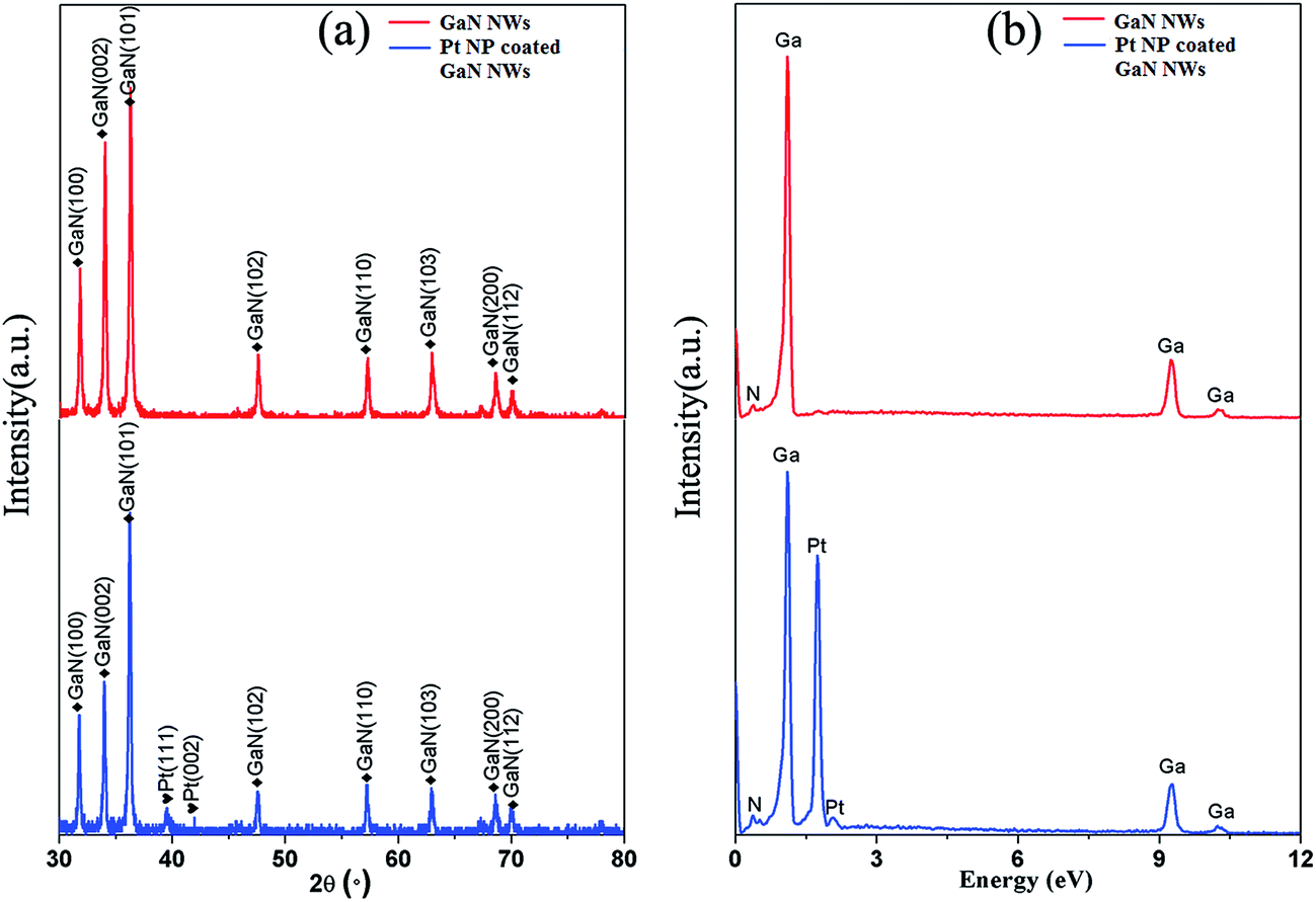
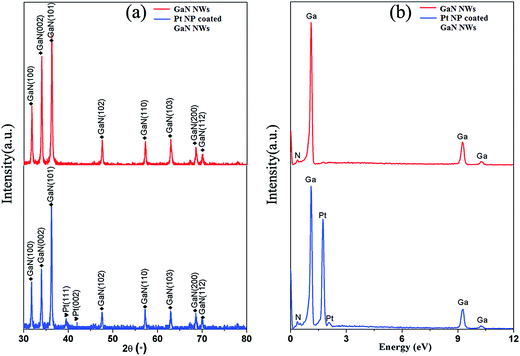
Fig. 1(a) shows the XRD pattern of pure GaN NWs and Pt NP coated GaN NWs. The diffraction peaks (100), (002), (101), (102), (110), (103), (200), and (112) are completely consistent with the standard card (Num. JCPDS 50-0792) of wurtzite hexagonal GaN.10 In addition, the weak peaks at 39.52° and 41.97° are attributed to the (111) and (200) plane of Pt in Fig. 1(a). Furthermore, Fig. 1(b) shows the EDS analysis of pure GaN NWs and Pt NP coated GaN NWs. EDS analysis of red line shows that the pure GaN NWs only consist of N and Ga elements, whereas blue line shows that Pt NP coated GaN NWs consist of N, Ga, and Pt elements. Both XRD and EDS indicate that the Pt coated GaN NWs have been synthesized.
 |
| | Fig. 1 (a) XRD and (b) EDS analysis of pure GaN NWs and Pt NP coated GaN NWs. | |
The SEM images of pure and Pt NP coated GaN NWs are shown in Fig. 2. Fig. 2(a and b) illustrate that the high density GaN NWs are grown on Si substrate, and the length of pure GaN NWs attains to several micrometers, moreover, the average diameter of pure GaN NWs is from 80 nm to 200 nm. Inset of Fig. 2(a) is side view of GaN NWs layer, which demonstrates the thickness of GaN NWs layer is 35 μm. Furthermore, Pt NPs are on the top of pure GaN NWs, which illustrates that the growth mechanism of GaN NWs is VLS mechanism.9 Compared with Fig. 2(b), it can be seen that NPs are attached on the top and surface of GaN NWs shown in Fig. 2(c and d). All the above results indicate that we have successfully synthesized Pt NP coated GaN NWs.
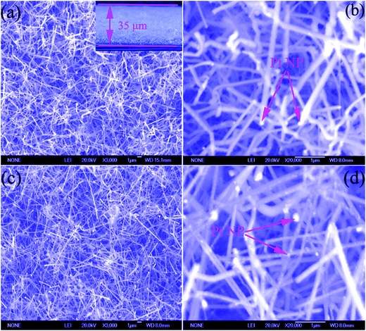 |
| | Fig. 2 (a) Low magnification and (b) high magnification SEM images of pure GaN NWs (inset of (a) is side view of GaN NWs layer); (c) low magnification and (d) high magnification SEM images of Pt NP coated GaN NWs. | |
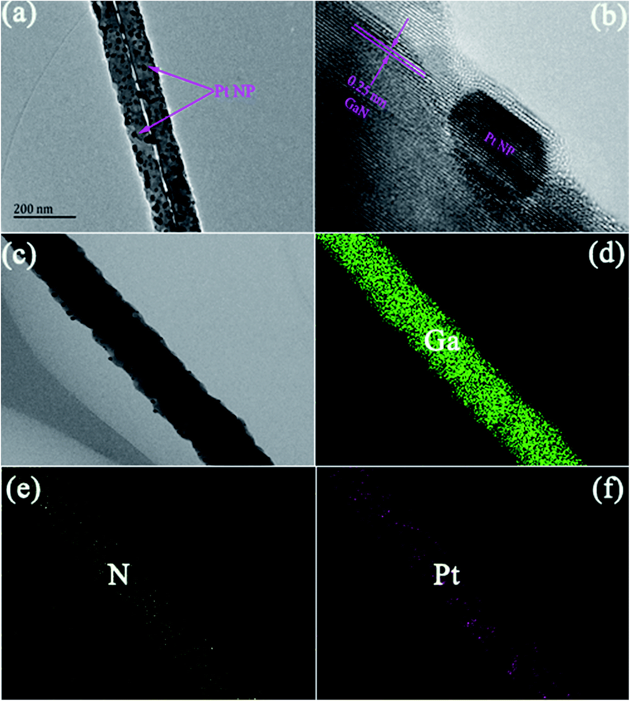
The TEM image of Pt NP coated GaN NWs is shown in Fig. 3(a), which demonstrates that Pt NPs have been adsorbed on the surfaces of GaN NWs. There are two parallel NWs, and the white line is the interspace between the two GaN NWs. The diameter of Pt NP is about 10 nm, and the diameter of Pt NP coated GaN NWs extends to 80 nm. In addition, the HRTEM image of Pt NP coated GaN NWs is shown in Fig. 3(b), which illustrates the lattice fringes with interplanar spacings of 0.25 nm, which is corresponding to the (002) planes of wurtzite GaN. Fig. 3(c–f) show that the spatially resolved elemental mapping of Pt NP coated GaN NWs gives a uniform distribution of Ga and N elements inside GaN NWs, and Pt elements distribute on the surfaces of GaN NWs.
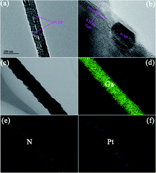 |
| | Fig. 3 (a) TEM and (b) HRTEM images of Pt NP coated GaN NWs; (c) STEM image of Pt NP coated GaN nanowire; and the elemental mapping of (d) Ga, (e) N, and (f) Pt. | |
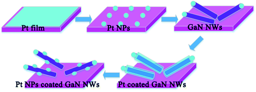
The schematic growth mechanism scheme of Pt NP coated GaN NWs is shown in Fig. 4. Firstly, Pt film with a thickness of 15 nm was sprayed onto Si substrate by sputter system. Secondly, Pt film was etched at 1000 °C with ammonia for 10 minutes, then, Pt-coated Si substrate was ready. Thirdly, the pure GaN NWs had been synthesized by VLS mechanism.9 Fourthly, Pt film was sprayed onto the surface of pure GaN NWs by sputter system. The thickness of Pt film is 15 nm. Fifthly, Pt coated GaN NWs was etched at 1000 °C with ammonia for 15 minutes, then, Pt NP coated GaN NWs had been synthesized.
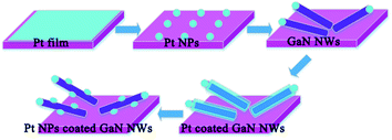 |
| | Fig. 4 The growth mechanism mode for Pt NP coated GaN NWs. | |
2.3 Field emission properties
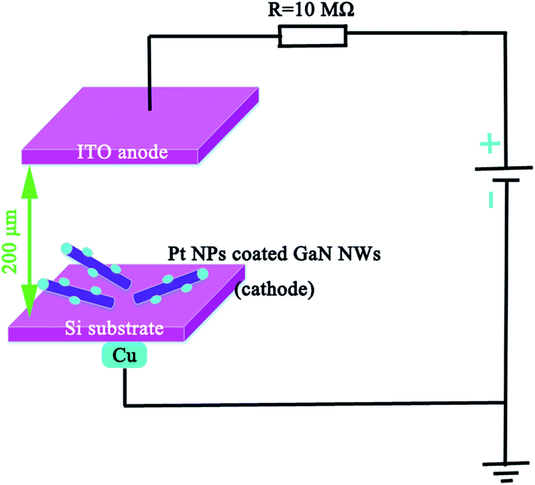
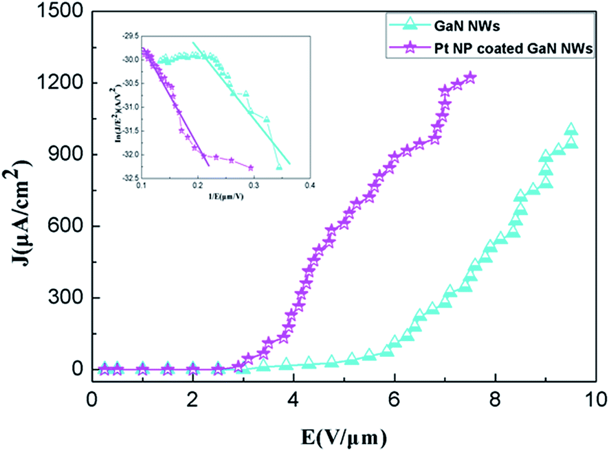
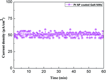
The schematic graphic of field emission measurement is shown Fig. 5. By definition, the threshold field is the electric field required to produce an emission current density of 1 mA cm−2, and the turn on field is the electric field required to produce an emission current density of 0.01 mA cm−2.22 Fig. 6 shows that the turn on field and threshold field are 3.3 V μm−1 and 9.5 V μm−1 from pure GaN NWs, moreover, the turn on field and threshold field are 2.7 V μm−1 and 6.8 V μm−1 from Pt NP coated GaN NWs. We can see that the F–N (ref. 23) plot inset in Fig. 6 are divided two parts. The one part is approximately linear, therefore the electron emission of the GaN NWs were accounted for vacuum tunneling effect.22 Another part is drift off the F–N line, which is because of the effect of the space charge and the absorbent.8 Knowing Φ of pure GaN NWs is 4.1 eV.24 The slope of the F–N plot shows that field-enhancement factor β of pure GaN NWs is around 2531. Since the surface morphologies of these two kinds of NWs are similar, we assume that β of Pt NP coated GaN NWs is also 2531. With this assumption, it is found that work function Φ of the Pt NP coated GaN NWs is 3.22 eV. In order to verify this hypothesis, we use the DFT to study the work function Φ of Pt adsorption GaN NWs. Fig. 7 shows the stability of Pt NP coated GaN NWs within 60 min under an applied electric field of 3.2 V μm−1. The initial current density is 48.34 μA cm−2 and the average current density is 50.76 μA cm−2. Current density is no notable degradation, and the emission current fluctuation is as low as ∼4.99%, proving the high stability of Pt NP coated GaN NWs as a field emitter.
 |
| | Fig. 5 Schematic diagram of our field-emission measurements. | |
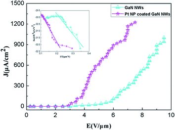 |
| | Fig. 6 Field emission J–E curve and F–N curve of pure GaN NWs and Pt NP coated GaN NWs. | |
 |
| | Fig. 7 Field emission current density stability of Pt NP coated GaN NWs. | |
3. Computational
3.1 Calculation methods and models
In this paper, electronic properties for Pt adsorbed GaN NWs have been simulated by first-principles DFT using Vienna ab initio simulation package.25 The generalized gradient approximation26 with the PW91 parameterization was adopted to describe the exchange–correlation interaction. The cutoff energy for the plane-wave basis set is 400 eV. The Brillouin zones were sampled by a set of k-points grid 1 × 1 × 5 using the Gamma centered Monkhorst–Pack scheme. All the atoms were fully relaxed until the convergence tolerance of the total energies from the last two sequential steps is less than 0.001 eV per atom as well as the maximum force on each atom is less than 0.001 eV Å−1.27
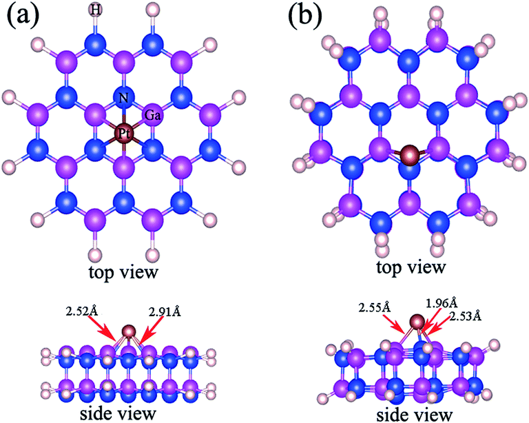
The initial structure of Pt adsorbed GaN NWs with 9.6 Å diameter along the 001 direction were generated from a bulk GaN supercell. The periodic boundary condition was applied along c axis and a sufficient vacuum space (12 Å) was imposed in a/b axis to ensure the NWs in neighboring supercells do not interact with each other. The crystal parameters are with lattice parameters of a = 3.189 Å, c = 5.185 Å,28 and the surface effect was eliminated through dangling bond hydrogenation passivation.29 The top view and side view of Pt adsorbed GaN NWs models are shown in Fig. 8(a). Furthermore, the model is pure GaN NWs if Pt atoms were deleted.
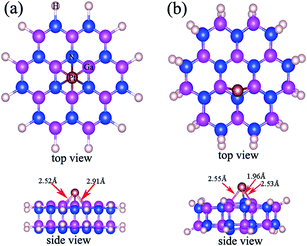 |
| | Fig. 8 (a) The top and side view of initial Pt adsorbed GaN NWs; (b) the top and side view of optimized Pt adsorbed GaN NWs. | |
3.2 Results and discussion
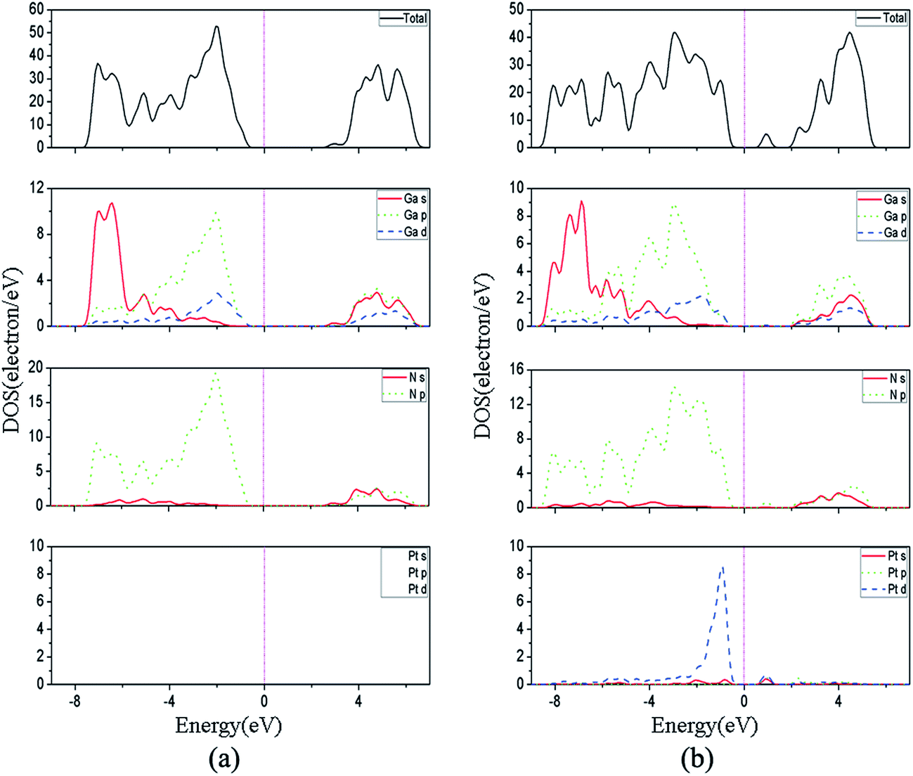
Fig. 8(b) shows the top view and side view of optimized structures of Pt adsorbed GaN NWs, which is similar to initial structure for pure GaN NWs. From Fig. 8, we can see that the Pt–Ga and Pt–N bond lengths are 2.52 Å and 2.91 Å for pure GaN NWs, whereas the Pt–Ga bond lengths range from 2.53 Å to 2.55 Å, moreover, the Pt–N bond length is 1.96 Å. Fig. 9 shows the total density of states and partial density of states (PDOSs) for pure and Pt adsorbed GaN NWs. The Fermi level is pointed out the pink dashed lines. PDOSs calculation reveals that the valence band maximum (VBM) of pure GaN nanowire is ruled by the N-2p orbital, and the conduction band minimum (CBM) is due to the Ga-4s and N-2s orbitals,27 as shown in Fig. 9(a). Fig. 9(b) illustrates that the VBM of Pt adsorbed GaN NW is ruled by the N-2p, Ga-4p, and Pt-5d orbitals, while the CBM is due to the Ga-4p, N-2s, and Pt-6p orbitals. The electron states distribute near the Fermi level, consequently, we conclude that the higher local electron states near the Fermi level will provide more electrons to the conduction band at a given operating voltage, and make the Pt adsorbed GaN NWs to possess some better field emission properties.27,30 The Φ is an important parameter to explain whether the field emission properties of GaN NWs are improved.31,32 Local density approximation exchange correlation functional is more suitable for Φ calculations,33 so the local density approximation has been used to investigate Φ. For one thing, Φ = 4.11 eV of pure GaN NWs is in excellent agreement with the experimental datum of Φ = 4.1 eV from ref. 22, for another thing, the Φ value of Pt adsorbed GaN NWs is 3.11 eV, which is close to the experiment result value (3.22 eV). In additional, we calculated the work function of GaN NWs with different adsorbed concentration, and the results indicate the work function of pair and triple Pt atoms adsorbed GaN NWs is 3.69 eV and 2.29 eV. So we can conclude the Pt adsorbed can improve the field emission performance of GaN NWs, and the high concentration is more effective for improvement the field emission performance. The reduction of Φ is induced by the donor states near the Fermi level, which is due to the N-2p, Pt-6s, and Pt-5d orbitals hybridization, thus, it means the enhancement of field emission performance of GaN NWs by Pt adsorbed.
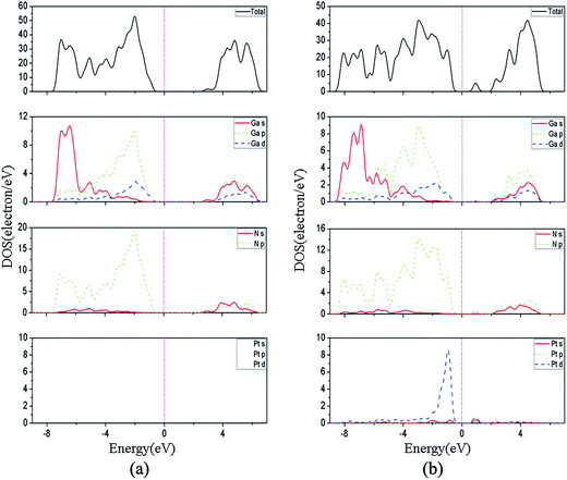 |
| | Fig. 9 (a) The DOS of pure GaN NWs; (b) the DOS of Pt adsorbed GaN NWs. | |
4. Conclusion
In summary, we have synthesized and studied field emission performance of Pt NP coated GaN NWs. The theoretical and experimental results confirm that Pt adsorbed can effectively boost the field emission performance of GaN NWs. Pt NPs were attached on the top and surfaces of the GaN NWs. With the Pt NP coated, it is found that the turn on field is reduced from 3.3 V μm−1 to 2.7 V μm−1 and the work function is decreased from 4.1 eV to 3.22 eV. These improvement could be attributed the higher local electron states near the Fermi level, it will provide more electrons to the conduction band at a given operating voltage. Consequently, Pt NP coated GaN NWs is promising for electron emission devices, field emission displays and vacuum nano-electronic devices.
Acknowledgements
This work was supported by the National Natural Science Foundation of China (No. 51042010), the Natural Science Key Project Foundation of Shaanxi Province, China (No. 2013JZ018).
References
- J. C. Zolper, R. J. Shul, A. G. Baca, R. G. Wilson, S. J. Pearton and R. A. Stall, Appl. Phys. Lett., 1996, 68, 2273 CrossRef CAS.
- Q. Chen, M. Asif Khan, J. W. Yang, C. J. Sun, M. S. Shur and H. Park, Appl. Phys. Lett., 1996, 69, 794 CrossRef CAS.
- F. A. Ponce and D. P. bour, Nature, 1997, 386, 351 CrossRef CAS.
- J. C. Johnson, H. J. Choi, K. P. Knutsen, R. D. Schaller, P. Yang and R. J. Saykally, Nat. Mater., 2002, 1, 106 CrossRef CAS PubMed.
- H. Yoshida, T. Urushido, H. Miyake and K. Hiramatsu, Jpn. J. Appl. Phys., 2001, 40, 1301 Search PubMed.
- D. K. T. Ng, M. H. Hong, L. S. Tan, Y. W. Zhu and C. H. Sow, Nanotechnology, 2007, 18, 375707 CrossRef.
- X. Xiang and H. Zhu, Appl. Phys. A, 2007, 87, 651 CrossRef CAS.
- E. L. Li, Z. Cui, Y. B. Dai, D. N. Zhao and T. Zhao, Appl. Surf. Sci., 2011, 257, 10850 CAS.
- Z. Cui, E. L. Li, W. Shi and D. M. Ma, Mater. Res. Bull., 2014, 56, 80 CrossRef CAS.
- Z. Cui, E. L. Li, W. Shi, D. M. Ma, T. Liu, X. Liu and G. S. Wu, Ceram. Int., 2015, 41, 6074 CrossRef CAS.
- G. Nabi, C. B. Cao, W. S. Kha, S. Hussain, Z. Usman, N. A. D. Khattak, Z. Ali, F. K. Butt, S. H. Shah and M. Safdar, Mater. Lett., 2012, 66, 50–53 CrossRef CAS.
- G. Nabi, C. Cao, W. S. Khan, S. Hussain, Z. Usman, T. Mahmood, N. A. D. Khattak, S. Zhao, X. Xin, D. Yu and X. Fu, Mater. Chem. Phys., 2012, 133, 793 CrossRef CAS.
- G. Nabi, C. Cao, W. S. Khan, S. Hussain, Z. Usman, M. Safdar and N. A. D. Khattak, Appl. Surf. Sci., 2011, 257, 10289 CrossRef CAS.
- E. L. Li, S. Song, D. M. Ma, N. Fu and Y. Zhang, J. Electron. Mater., 2014, 43, 1379 CrossRef CAS.
- E. L. Li, Z. Cui, N. Fu, R. Xu and D. M. Ma, Mater. Lett., 2015, 15, 426 CrossRef.
- L. T. Fu, Z. G. Chen, D. W. Wang, L. Cheng, H. Y. Xu, J. Z. Liu, H. T. Cong, G. Q. Lu and J. Zou, J. Phys. Chem. C, 2010, 114, 9627 CAS.
- B. Liu, Y. Bando, C. Tang, F. Xu and D. Golberg, Appl. Phys. Lett., 2005, 87(7), 073106 CrossRef.
- T. Yamashita, S. Hasegawa, S. Nishida, M. Ishimaru, Y. Hirotsu and H. Asahi, Appl. Phys. Lett., 2005, 86(8), 082109 CrossRef.
- C. C. Tang, X. W. Xu, L. Hu and Y. X. Li, Appl. Phys. Lett., 2009, 94, 3105 Search PubMed.
- T. Y. Tsai, S. J. Chang, W. Y. Weng, S. Li, S. Liu, C. L. Hsu and T. J. Hsueh, IEEE Electron Device Lett., 2013, 34, 553 CrossRef CAS.
- E. L. Li, G. S. Wu, Z. Cui, D. M. Ma, W. Shi and X. L. Wang, Nanotechnology, 2016, 27, 265707 CrossRef PubMed.
- G. Nabi, C. B. Cao, S. Hussain, W. S. Khan, R. R. Sagar, Z. Ali, F. K. Butt, Z. Usman and D. Yu, CrystEngComm, 2012, 14, 8492 RSC.
- R. H. Fowler and L. W. Nordheim, Proc. R. Soc. London, Ser. A, 1928, 119, 173 CrossRef CAS.
- B. Liu, Y. Bando, C. Tang, F. Xu, J. Hu and D. Golberg, J. Phys. Chem. B, 2005, 109, 17082 CrossRef CAS PubMed.
- G. Kresse and J. Furthmüller, Comput. Mater. Sci., 1996, 6, 15–50 CrossRef CAS.
- J. P. Perdew, K. Burke and M. Ernzerhof, Phys. Rev. Lett., 1996, 77, 3865 CrossRef CAS PubMed.
- Z. Cui, X. Ke, E. L. Li and T. Liu, Mater. Des., 2016, 96, 409 CrossRef CAS.
- H. Schulz and K. H. Thiemann, Solid State Commun., 1977, 23, 815–821 CrossRef CAS.
- D. J. Carter, J. D. Gale, B. Delley and C. Stampfl, Phys. Rev. B: Condens. Matter Mater. Phys., 2008, 77, 115349 CrossRef.
- C. Kim, B. Kim, S. M. Lee, C. Jo and Y. H. Lee, Phys. Rev. B: Condens. Matter Mater. Phys., 2002, 65, 165418 CrossRef.
- F. Buonocore, F. Trani, D. Ninno, A. Di Matteo, G. Cantele and G. Iadonisi, Nanotechnology, 2008, 19, 025711 CrossRef CAS PubMed.
- A. Wei, X. J. Wu and X. C. Zeng, J. Phys. Chem. B, 2006, 110, 16346 CrossRef PubMed.
- W. Liu, W. T. Zheng and Q. Jiang, Phys. Rev. B: Condens. Matter Mater. Phys., 2007, 75, 235322 CrossRef.
|
| This journal is © The Royal Society of Chemistry 2017 |
Click here to see how this site uses Cookies. View our privacy policy here. 
 Open Access Article
 This Open Access Article is licensed under a
  *a,
Xizheng Kea,
Enling Lia,
Taifei Zhao*a,
Qingping Qia,
Jie Yana,
Yingchun Dingb and
Tong Liuc
*a,
Xizheng Kea,
Enling Lia,
Taifei Zhao*a,
Qingping Qia,
Jie Yana,
Yingchun Dingb and
Tong Liuc