DOI:
10.1039/C7RA02485A
(Paper)
RSC Adv., 2017,
7, 23301-23308
Heat-up synthesis of Cu2SnS3 quantum dots for near infrared photodetection
Received
28th February 2017
, Accepted 21st April 2017
First published on 27th April 2017
Abstract
Cu2SnS3 quantum dots in the size range of 2.7 nm to 3.6 nm were synthesized using a solution based heat up method. The structural, optical and electrical properties were studied using X-ray diffraction, transmission electron microscopy, UV-Vis spectroscopy, X-ray photoelectron spectroscopy and cyclic voltammetry. In this paper we report, the infrared photo detection of Cu2SnS3 quantum dots. The responsivity, external quantum efficiency and specific detectivity were measured for the infrared lamp under different applied biases and for different illumination intensities of the 1550 nm and 1064 nm lasers. The responsivity, external quantum efficiency and specific detectivity exhibited high values of 1.76 A W−1, 272.53% and 2.79 × 10¹¹ Jones at −0.5 V applied bias, under infrared lamp illumination intensity of 0.48 W cm−2.
Introduction
Colloidal quantum dots (QDs) have found exquisite applications in a variety of optoelectronic devices such as photovoltaics,1–3 light emitting diodes4–6 and photodetectors.7–9 They have unique properties like band gap tunability and high absorption due to increased surface to volume ratio.10 Infrared (IR) detectors are used in night vision cameras, biomedical imaging and optical fibre communication.11,12 Generally materials like CdTe, Hg1−xCdxTe and CuIn1−xAlxSe2 (ref. 12–14) have been used for IR detection. However the toxicity of Cd and Hg15,16 as well as the rarity and high cost of Te and In17,18 have prompted the lookout for earth abundant, inexpensive and non toxic materials for photodetection. Cu2SnS3 (CTS) is a newly researched material which satisfies the above required properties. It is a p type semiconductor having a high absorption coefficient of 104 cm−1 and a band gap lying in the near IR range19 which makes it an ideal material for IR photo detection.
Usage of solution processable techniques leads to economic, easy and large area deposition of thin films. The heat up method is very useful for large scale production of quantum dots. The size of the quantum dots can be increased by increasing the reaction time, thus providing an easy control on the size of the quantum dots.20 In our previous report we have studied the application of CTS thin films in visible-IR photo detection.21 In this paper we have demonstrated the use of CTS QDs in IR photo detection.
Experimental
Synthesis
The CTS QDs were synthesized using heat up method. 1 mmol tin(IV) acetate, 2 mmol CuI and 3 mmol 1-dodecanethiol (DDT) were taken in a three necked round bottom flask and the reaction mixture was degassed under vacuum for 5 min and purged with argon gas three times. Here, DDT acts as a solvent, sulfur source as well as the capping agent hence controlling the dimensions of the QD and its growth. This allows us to avoid the use of extra precursors. After heating the flask to 100 °C for 10 min, the temperature was raised to 230 °C. With increase in temperature, the colour of the reaction mixture progressed from yellow to red and finally to black, marking the nucleation and subsequent growth of the CTS QDs. The product was collected after 5, 10, 20, 30, 40 and 50 minutes of the reaction. The QDs were separated from the product by precipitation using acetone followed by centrifugation and decanting. The reaction involved in this process is hypothesized as shown below
Device fabrication
Flexible In doped SnO2 (ITO) coated polyethylene terephthalate (PET) 1 × 1.5 cm2 sized substrates (surface resistivity 60 Ω sq−1) were used. The substrates were sequentially cleaned by sonicating in deionised water and isopropyl alcohol and later flushed with nitrogen gas. The CTS quantum dots were dispersed in ethanol (0.13 g ml−1) and the solution was spin coated at 500 rpm for 90 s. This was repeated for 15 coatings. The silver electrical contacts were deposited by thermal evaporation.
Characterization
Phase formation was confirmed by X-ray diffraction (XRD) using a PANalytical X'Pert PRO Diffractometer equipped with a Cu Kα source of 1.5405 Å wavelength. The absorbance spectrum was measured using UV-Vis-NIR spectrophotometer (Perkin Elmer-Lambda 750). The morphology of the quantum dots was observed using transmission electron microscopy (TEM, Jeol JEM-2100F) at an accelerating voltage of 200 kV. X-ray photoelectron spectroscopy (XPS) was measured using AXIS UltraDLD X-ray photoelectron spectrometer with Al Kα X-ray source. Raman spectroscopy was studied using Raman spectrometer (LabRAM HR) with 514 nm line of Ar+ laser. Cyclic voltammetry was measured after dropcasting the CTS quantum dots onto glassy carbon working electrode. Pt and Ag/AgCl were used as the counter and reference electrodes respectively. An electrolyte of 0.1 M KOH in D.I. water was used. The voltage was scanned at a rate of 0.1 V s−1. The dark and photocurrent measurements were taken using Keithley source measure unit SMU 2420. Noise measurements were taken in dark and at room temperature using a Stanford Research SR 830 lock-in amplifier in the current measurement mode.
Results and discussion
Fig. 1 shows the XRD pattern for CTS quantum dots taken at different growth time intervals. The XRD pattern matches well with the JCPDS 0894714. With increase in the reaction time, the intensity of the XRD peaks is found to increase which is due to growth in the particle size with time. All batches of quantum dots were found to have tetragonal crystal structure.
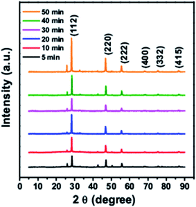 |
| | Fig. 1 XRD of the CTS QD cores at different reaction times. | |
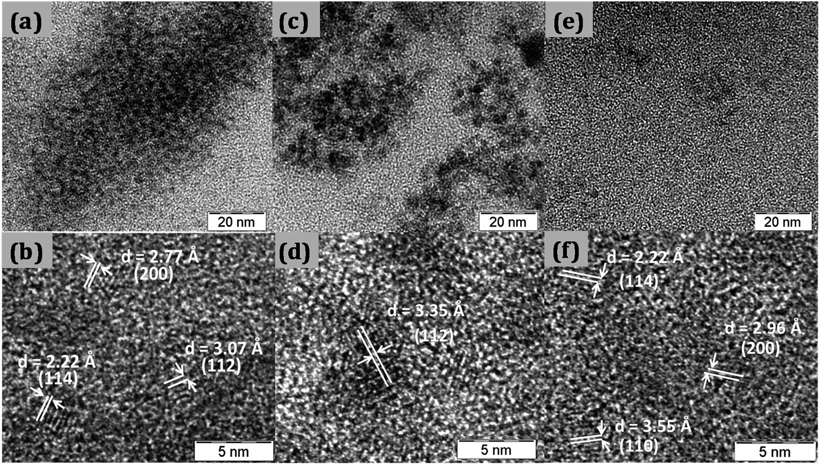
TEM images of synthesized quantum dots are shown in Fig. 2. The quantum dots sizes were found to be around 2.7 nm, 3.3 nm and 3.6 nm at 5 min, 10 min and 30 min reaction times respectively as shown in Fig. 2a–c. From the high resolution TEM images (Fig. 2b, d and f) the interplanar spacings were calculated and they matched with the tetragonal crystal structure of CTS.
 |
| | Fig. 2 TEM images of the CTS quantum dots at 5 min, 10 min and 30 min reaction times. | |
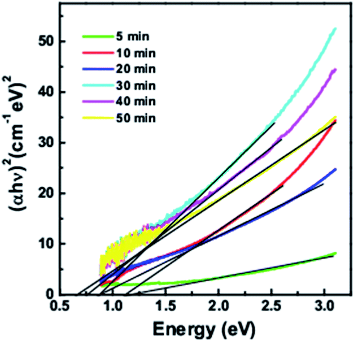
Fig. 3 shows the band gaps calculated from Tauc plots of (αhν)2 versus hν for quantum dots taken at different time intervals. The band gaps vary from 1.26 eV, 1.15 eV, 0.92 eV, 0.89 eV, 0.76 eV and 0.69 eV for 5 min, 10 min, 20 min, 30 min, 40 min and 50 min growth time respectively. With increase in the reaction time, the quantum dot size increases and hence there is a decrease in the bandgap.
 |
| | Fig. 3 Band gaps calculated from Tauc plot for CTS quantum dots at different growth time intervals. | |
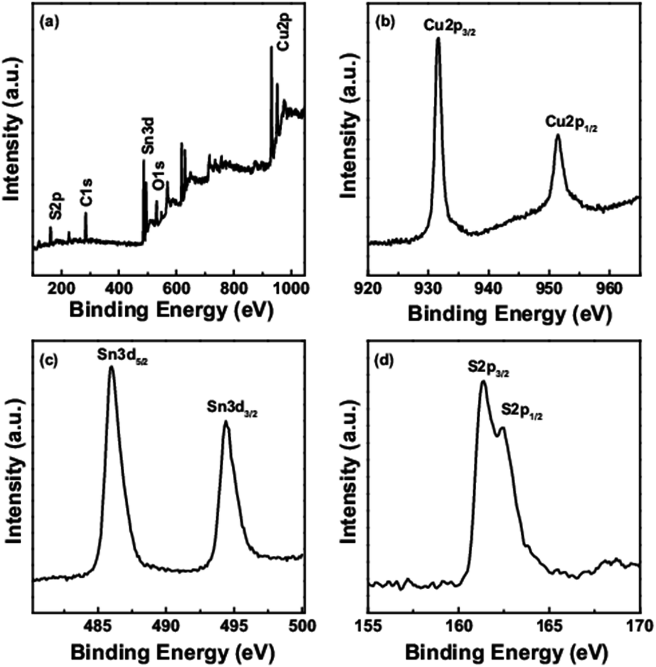
XPS was used to determine the valence states and composition of the CTS quantum dots. The survey spectra (Fig. 4a) shows the presence of Cu, Sn, S, C and O elements. Presence of oxygen and carbon could be due to the environment. Fig. 4b–d represent the core level spectra of Cu 2p, Sn 3d and S 2p. The binding energies for Cu 2p3/2 and Cu 2p1/2 were at 931.7 eV and 951.5 eV respectively corresponding to the +1 oxidation state of Cu.22 There is no peak at 942 eV corresponding to the +2 oxidation of Cu.23 The binding energies for Sn 3d5/2 and Sn 3d3/2 were at 486 eV and 494.4 eV respectively corresponding to the +4 oxidation state of Sn.24 The binding energies for S 2p3/2 and S 2p1/2 were at 161.4 eV and 162.5 eV respectively corresponding to the −2 oxidation state of S.25
 |
| | Fig. 4 X-Ray photoelectron spectra of the CTS quantum dots (a) survey spectrum (b) Cu 2p (c) Sn 3d (d) S 2p core level spectra. | |
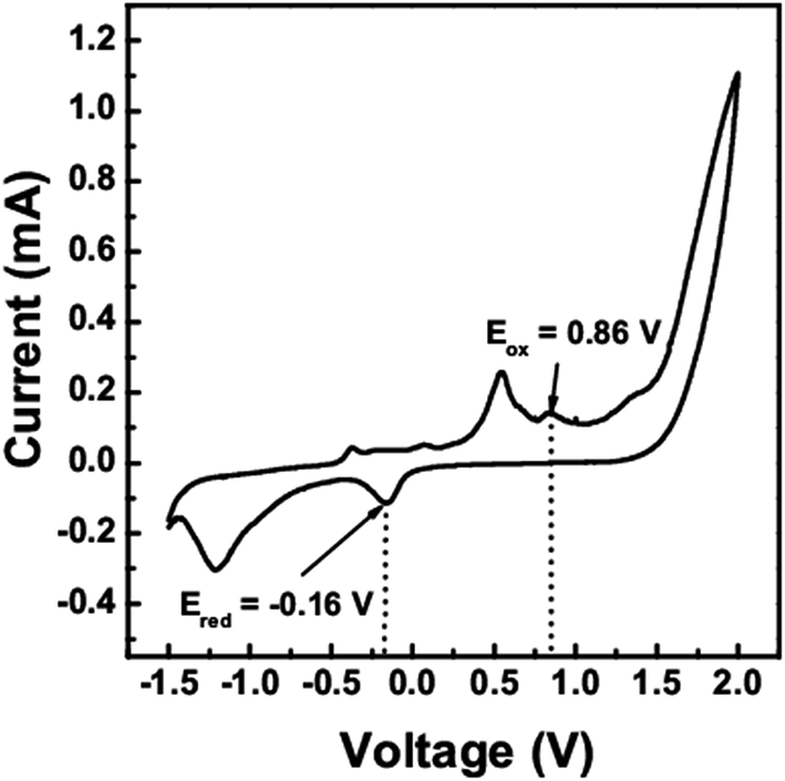
Cyclic voltammetry (CV) can be used to determine the band gap and the energy levels of the valence band and conduction band of semiconductors, i.e. the (highest occupied molecular orbital) HOMO and (lowest unoccupied molecular orbital) LUMO levels from the measurement of the reduction and oxidation potentials. The CV scan of the CTS quantum dots (10 min) was taken between −1.5 V to 2 V as shown in Fig. 5. The HOMO (or ionization potential Ip) and LUMO (or electron affinity Ea) levels were calculated using the eqn (1) and (2), where Eox is the onset oxidation potential and Ered is the onset reduction potential26
| | |
EHOMO = −Ip = −(Eox + 4.71) eV
| (1) |
| | |
ELUMO = −Ea = −(Ered + 4.71) eV
| (2) |
 |
| | Fig. 5 Cyclic voltammetry scan of the CTS quantum dots. | |
From the oxidation and reduction peaks in the CV scan, the oxidation and reduction potentials were found to be 0.86 V and −0.16 V respectively. On substituting these values in the above equations, the HOMO and LUMO levels were found to be at −5.57 eV and −4.55 eV respectively. The electrochemical band gap of the CTS quantum dots was found to be 1.02 eV. This value is a little higher than the optical band gap by 0.13 eV.
Fig. 6 shows the energy band diagram for the ITO/CTS/Ag device constructed using the HOMO and LUMO levels for CTS determined using cyclic voltammetry.
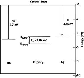 |
| | Fig. 6 Energy band diagram of the CTS QDs as determined from cyclic voltammetry along with the ITO and Ag work function levels. | |
Photo detection
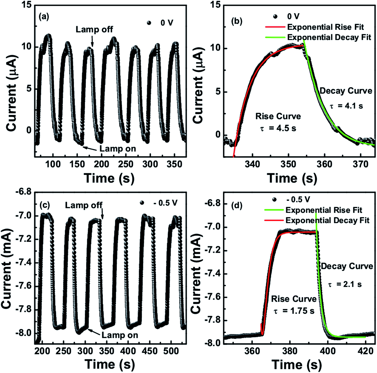
Fig. 7(a) and (c) show the time dependent photoresponse of the CTS photodetector under IR lamp illumination intensity of 0.48 W cm−2 taken at 0 V and −0.5 V bias respectively. The transient photoresponse was measured for several on–off cycles of the lamp. The curve proves the stability and reversibility of the detector device. It was observed that the growth and decay curves of the photocurrent followed the first order exponential behavior. The rise and decay curves are shown in Fig. 7(b) and (d) at 0 V and −0.5 V bias voltage respectively, both were fitted to the first order exponential equations I(t)rise = Idark + A![[thin space (1/6-em)]](https://www.rsc.org/images/entities/char_2009.gif) exp[t/τrise] and I(t)decay = Idark + Aexp[−t/τdecay] to determine the rise and decay time constants, where I(t) is the photocurrent at time t, Idark is the dark current, A is a scaling constant, τ is the time constant and t is the time when the lamp was switched on and off. At 0 V, the time constant for rise and decay curves were calculated as 4.5 seconds and 4.1 seconds respectively, whereas at −0.5 voltage it was 1.75 and 2.1 seconds. The photo-detector device was also tested under the 1064 nm and 1550 nm laser illumination at different intensities. It was observed that with increasing the intensity of laser the current increases which is due to the increased exciton generation with increased photon impingement.
exp[t/τrise] and I(t)decay = Idark + Aexp[−t/τdecay] to determine the rise and decay time constants, where I(t) is the photocurrent at time t, Idark is the dark current, A is a scaling constant, τ is the time constant and t is the time when the lamp was switched on and off. At 0 V, the time constant for rise and decay curves were calculated as 4.5 seconds and 4.1 seconds respectively, whereas at −0.5 voltage it was 1.75 and 2.1 seconds. The photo-detector device was also tested under the 1064 nm and 1550 nm laser illumination at different intensities. It was observed that with increasing the intensity of laser the current increases which is due to the increased exciton generation with increased photon impingement.
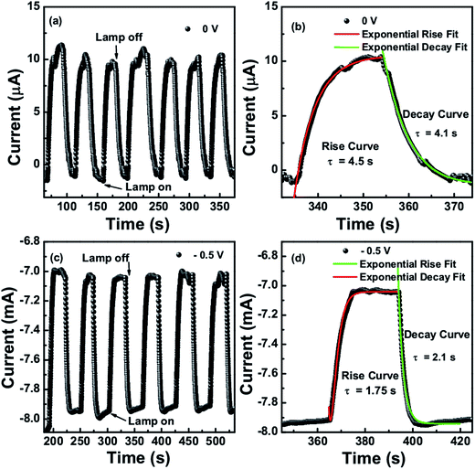 |
| | Fig. 7 (a and c) Time dependent photoresponse (b and d) rise and decay curve fits for IR lamp illumination intensity of 0.48 W cm−2 at 0 and −0.5 V respectively. | |
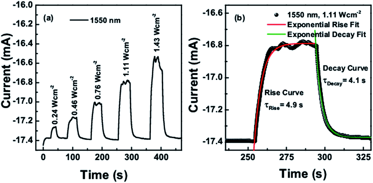
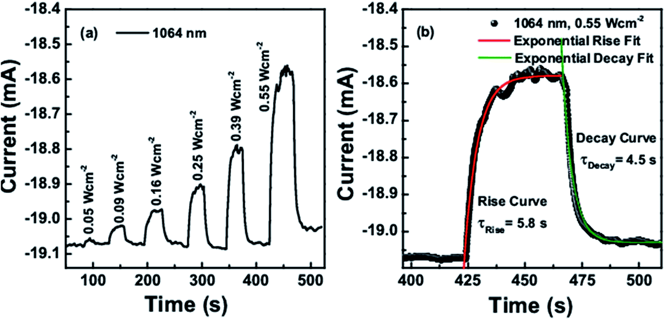
The obtained on–off cycles of I–t curves are shown in Fig. 8a and 9a. The rise and decay curves as shown in Fig. 8b for 1550 nm laser (intensity 1.11 W cm−2) and Fig. 9b for 1064 nm laser (intensity 0.55 W cm−2), both were exponentially fitted to the first order equation to determine the rise and decay time constants. For 1550 nm laser, the time constant for rise and decay curves were calculated as 4.9 s and 4.1 s respectively, whereas for 1064 nm laser, it was 5.8 s and 4.5 s.
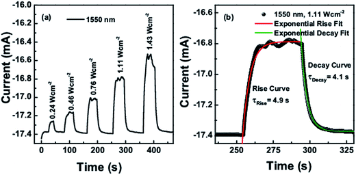 |
| | Fig. 8 (a) Time dependent photoresponse at different illumination intensities of the 1550 nm laser under −1 V applied bias (b) plot showing the exponential rise and decay fits to extract the decay constants. | |
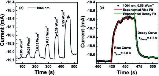 |
| | Fig. 9 (a) Time dependent photoresponse at different illumination intensities of the 1064 nm laser under −1 V applied bias (b) plot showing the exponential rise and decay fits to extract the decay constants. | |
Photodetection mechanism
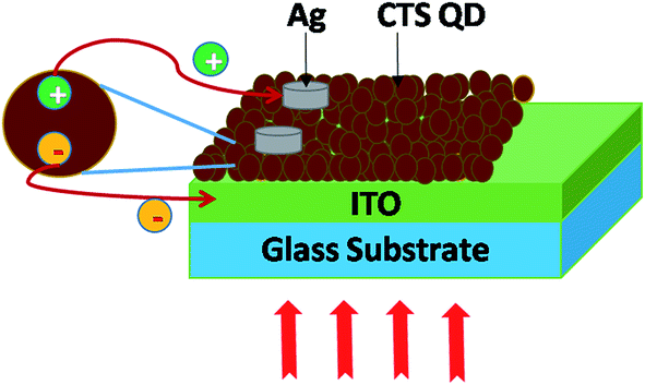
The time dependent photoresponse of the CTS QDs was measured under dark and illumination conditions. Initially in dark, there is some current due to the charge carriers present within the material. Then the material gets depleted of charges leading to the formation of a depletion region. When light is shined on the material, there is formation of electrons and holes in the depletion region. The charge carriers get separated and the electrons are transported to the ITO electrode and the holes are transferred to the Ag electrode leading to the generation of photocurrent. Fig. 10 depicts the schematic of the device architecture and the mechanism of electron hole pair generation and separation in the CTS QD photodetector.
 |
| | Fig. 10 Device structure of the CTS QD photodetector and the mechanism of charge transfer. | |
The various parameters such as responsivity, external quantum efficiency and specific detectivity were calculated. The responsivity Rλ of the device defined by Rλ = Iλ/PλS, is the amount of photocurrent generated per unit illumination intensity, per unit area.27 Here Iλ is the photocurrent given by Iλ = Ilight − Idark, Pλ is the illumination intensity and S is the effective area of illumination. The external quantum efficiency EQE defined as the number of electrons generated per incident photon is given by EQE = hcRλ/qλ, where h is Planck's constant, c is the velocity of light, q is the electronic charge and λ is the wavelength of the light source. The specific detectivity D* is the ability of a photodetector to detect the smallest light signal and is given by D* = (AΔf)1/2Rλ/in, where A is the device area = 0.1 mm2, Δf is the frequency band width = 3333.33 Hz, Rλ is the responsivity and in = 11.9 pA is the value of the noise current obtained using noise measurements.28
The calculated values of various parameters like responsivity, EQE and specific detectivity are shown in Table 1 for the IR lamp at different applied biases and in Tables 2 and 3 for 1550 nm and 1064 nm laser illuminations respectively at different intensities.
Table 1 The calculated values of responsivity, EQE and specific detectivity under IR lamp illumination of 0.48 W cm−2
| Bias (V) |
R (A W−1) |
EQE% |
D* Jones |
| 0 |
0.02 |
3.39 |
3.47 × 10⁹ |
| −0.5 |
1.76 |
272.53 |
2.79 × 10¹¹ |
Table 2 The calculated values of responsivity, EQE and specific detectivity under 1550 nm laser illumination
| Illumination intensity (W cm−2) |
R (A W−1) |
EQE% |
D* Jones |
| 0.24 |
0.47 |
37.63 |
7.47 × 10¹⁰ |
| 0.46 |
0.45 |
35.68 |
7.08 × 10¹⁰ |
| 0.76 |
0.46 |
37.24 |
7.39 × 10¹⁰ |
| 1.11 |
0.51 |
40.98 |
8.14 × 10¹⁰ |
| 1.43 |
0.55 |
44.42 |
8.81 × 10¹⁰ |
| 1.98 |
0.60 |
48.16 |
9.56 × 10¹⁰ |
Table 3 The calculated values of responsivity, EQE and specific detectivity under 1064 nm laser illumination
| Illumination intensity (W cm−2) |
R (A W−1) |
EQE% |
D* Jones |
| 0.05 |
0.54 |
62.91 |
8.57 × 10¹⁰ |
| 0.09 |
0.67 |
77.82 |
1.06 × 10¹¹ |
| 0.16 |
0.66 |
76.57 |
1.04 × 10¹¹ |
| 0.25 |
0.69 |
80.18 |
1.09 × 10¹¹ |
| 0.39 |
0.71 |
82.35 |
1.12 × 10¹¹ |
| 0.55 |
0.89 |
103.58 |
1.41 × 10¹¹ |
From Tables 1–3 with application of bias and on increasing the laser intensity all the parameters responsivity, EQE, and specific detectivity were found to increase.
The values of responsivity, EQE and specific detectivity measured at 0 V and −0.5 V applied bias in the present paper for CTS QDs by heat up technique is greater than the values mentioned in previous papers for 3, 1 and 0 V bias respectively for CTS thin film, nanostructures and QDs by solvothermal method (Table 4). The increase in the photoresponse parameters of the CTS QDs synthesized by heat up method in the present paper could be due to the increased surface to volume ratio of the QDs owing to its smaller dimensions when compared to thin films or nanostructures. This leads to increased absorption of light and easier charge separation and collection due to increased interfacial area, thus leading to higher photocurrent and higher photoresponse. Also when compared to solvothermal method, heat up technique is a more efficient and economical way of obtaining QDs of different sizes from one reaction mixture within a short time of about few minutes, whereas in solvothermal method each reaction takes about certain hours.
Table 4 Comparison of photo detection parameters under IR illumination
| Sample |
Intensity (mW cm−2) |
R (mA W−1) |
EQE% |
D* Jones |
Ref. |
| CTS thin film |
477.7 (750–1100 nm) |
16.32 |
2.53 |
5.1 × 10¹⁰ |
21 |
| CTS nanostructures |
477.7 (750–1100 nm) |
0.46 |
0.071 |
2.2 × 10⁹ |
29 |
| CTS (QDs-solvothermal method) |
477.7 (750–1100 nm) |
7.66 |
1.19 |
2.1 × 10¹⁰ |
30 |
| Cu2ZnSnS4 |
−(1064 nm) |
13 |
15 |
— |
31 |
| Cu3BiS3 |
60 (1064 nm) |
1040 |
1.21 |
— |
32 |
| Cu2CoSnS4 |
50 (1064 nm) |
126 |
14.74 |
— |
33 |
| CuIn1−xAlxSe2 |
790 nm (cut off) |
490 |
— |
— |
12 |
| Hg1−xCdxTe |
— |
— |
— |
3 × 10¹⁰ |
34 |
| Si |
(1200 nm) |
14.5 |
— |
— |
35 |
| (1300 nm) |
0.433 |
When we compare the values of the photo detection parameters obtained in the present work with the values for other materials in Table 4, we can see that the values obtained in our case is either comparable or higher than the values for other materials. We can further improve the device in order to decrease the response time i.e. to make a faster detector.
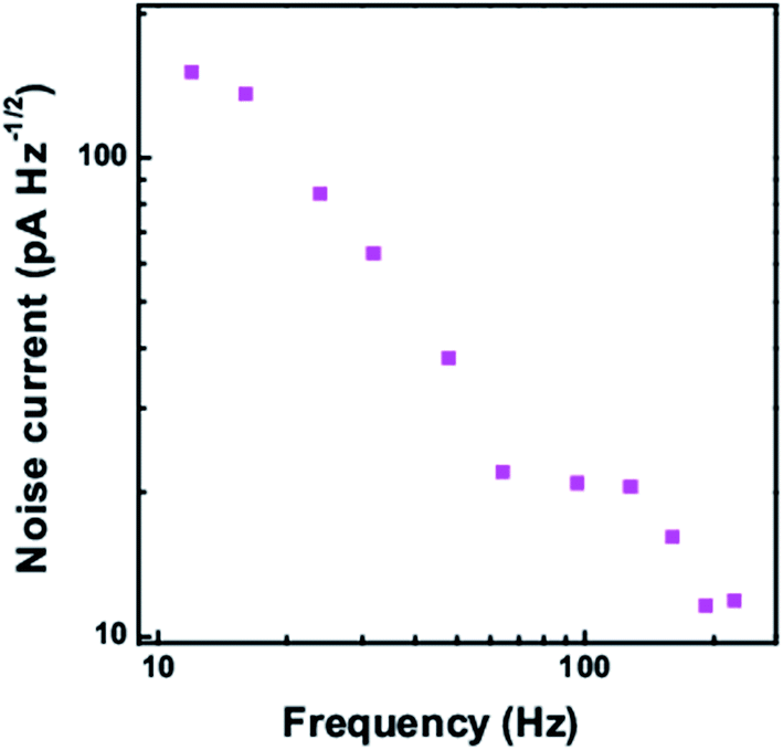
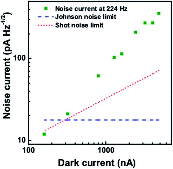
The noise current at different frequencies is shown in Fig. 11 at a dark current of 159.87 nA. With increase in frequency, the noise current is found to decrease. Also the noise current at a frequency of 224 Hz for different dark current levels is shown in Fig. 12. With increase in the dark current, the noise current is also found to increase. The Shot noise and the Johnson noise are also plotted for comparison.
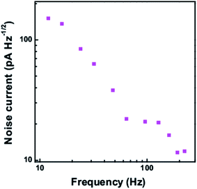 |
| | Fig. 11 Noise current versus frequency measured at a dark current of 159.87 nA. | |
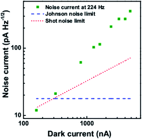 |
| | Fig. 12 Noise current versus dark current at 224 Hz. | |
Conclusions
CTS quantum dots were synthesized by the solution processed heat up method. The structural, optical and electrical properties were deduced. The IR photoresponse of the quantum dots incorporated devices were tested under IR lamp, 1550 nm and 1064 nm lasers. The responsivity, external quantum efficiency and specific detectivity were compared under different biases and illumination intensities. The present work showed a significant improvement in the photoresponse parameters when compared to the previous reports.
Acknowledgements
The authors would like to thank Mr Debanjan Das from Prof. K. K. Nanda's group (Materials Research Centre, IISc) for helping in the cyclic voltammetry measurements. Also we would like to thank Ms Ramya from Prof. Aveek Bid's group (Physics Dept., IISc) for helping in the noise measurements.
References
- C.-H. M. Chuang, P. R. Brown, V. Bulović and M. G. Bawendi, Nat. Mater., 2014, 13, 796 CrossRef CAS PubMed.
- J. Zhang, J. Gao, E. M. Miller, J. M. Luther and M. C. Beard, ACS Nano, 2014, 8, 614 CrossRef CAS PubMed.
- D. H. Jara, S. J. Yoon, K. G. Stamplecoskie and P. V. Kamat, Chem. Mater., 2014, 26, 7221 CrossRef CAS.
- J. Chen, D. Zhao, C. Li, F. Xu, W. Lei, L. Sun, A. Nathan and X. W. Sun, Sci. Rep., 2014, 4, 4085 CrossRef PubMed.
- W.-S. Song and H. Yang, Chem. Mater., 2012, 24, 1961 CrossRef CAS.
- X. Gong, Z. Yang, G. Walters, R. Comin, Z. Ning, E. Beauregard, V. Adinolfi, O. Voznyy and E. H. Sargent, Nat. Photon., 2016, 10, 253 CrossRef CAS.
- J. P. Clifford, G. Konstantatos, K. W. Johnston, S. Hoogland, L. Levina and E. H. Sargent, Nat. Nanotechnol., 2009, 4, 40 CrossRef CAS PubMed.
- E. Lhuillier, M. Scarafagio, P. Hease, B. Nadal, H. Aubin, X. Z. Xu, N. Lequeux, G. Patriarche, S. Ithurria and B. Dubertret, Nano Lett., 2016, 16, 1282 CrossRef CAS PubMed.
- K. Qiao, H. Deng, X. Yang, D. Dong, M. Li, L. Hu, H. Liu, H. Song and J. Tang, Nanoscale, 2016, 8, 7137 RSC.
- Z. Ning, O. Voznyy, J. Pan, S. Hoogland, V. Adinolfi, J. Xu, M. Li, A. R. Kirmani, J.-P. Sun, J. Minor, K. W. Kemp, H. Dong, L. Rollny, A. Labelle, G. Carey, B. Sutherland, I. Hill, A. Amassian, H. Liu, J. Tang, O. M. Bakr and E. H. Sargent, Nat. Mater., 2014, 13, 822 CrossRef CAS PubMed.
- M. Izzetoglu, S. C. Bunce, K. Izzetoglu, B. Onaral and A. K. Pourrezaei, IEEE Eng. Med. Biol. Mag., 2007, 26, 38 CrossRef PubMed.
- R.-P. Chang and D.-C. Perng, Appl. Phys. Lett., 2011, 99, 081103 CrossRef.
- X. Xie, S.-Y. Kwok, Z. Lu, Y. Liu, Y. Cao, L. Luo, J. A. Zapien, I. Bello, C.-S. Lee, S.-T. Lee and W. Zhang, Nanoscale, 2012, 4, 2914 RSC.
- J. Yang, Y. Zhou, S. Zheng, X. Liu, X. Qiu, Z. Tang, R. Song, Y. He, C. W. Ahn and J. W. Kim, Chem. Mater., 2009, 21, 3177 CrossRef CAS.
- P. Das, S. Samantaray and G. R. Rout, Environ. Pollut., 1997, 98, 29 CrossRef CAS PubMed.
- L. Magos and T. W. Clarkson, Ann. Clin. Biochem., 2006, 43, 257 CrossRef CAS PubMed.
- B. L. Cohen, Geochim. Cosmochim. Acta, 1984, 48, 203 CrossRef CAS.
- G. Phipps, C. Mikolajczak and T. Guckes, Refocus, 2008, 9, 56 Search PubMed.
- P. A. Fernandes, P. M. P. Salomé and A. F. d. Cunha, J. Phys. D: Appl. Phys., 2010, 43, 215403 CrossRef.
- Q. Liang, L. Han, X. Deng, C. Yao, J. Meng, X. Liu and J. Meng, CrystEngComm, 2014, 16, 4001 RSC.
- S. Dias and S. B. Krupanidhi, AIP Adv., 2016, 6, 025217 CrossRef.
- X. Liang, Q. Cai, W. Xiang, Z. Chen, J. Zhong, Y. Wang, M. Shao and Z. Li, J. Mater. Sci. Technol., 2013, 29, 231 CAS.
- L. D. Partain, R. A. Schneider, L. F. Donaghey and P. S. McLeod, J. Appl. Phys., 1985, 57, 5056 CrossRef CAS.
- A. R. H. F. Ettema and C. Hass, J. Phys.: Condens. Matter, 1993, 5, 3817 CrossRef CAS.
- I. Nakai, Y. Sugitani, K. Nagashima and Y. Niwa, J. Inorg. Nucl. Chem., 1978, 40, 789 CrossRef CAS.
- Y. C. Li, H. Z. Zhong, R. Li, Y. Zhou, C. H. Yang and Y. F. Li, Adv. Funct. Mater., 2006, 16(13), 1705 CrossRef CAS.
- J. Ding, H. Fang, Z. Lian, J. Li, Q. Lv, L. Wang, J.-L. Sun and Q. Yan, CrystEngComm, 2016, 18, 440 Search PubMed.
- L. Dou, Y. Yang, J. You, Z. Hong, W.-H. Chang, G. Li and Y. Yang, Nat. Commun., 2014, 5, 5404 CrossRef CAS PubMed.
- S. Dias and S. B. Krupanidhi, J. Nanosci. Nanotechnol., 2017, 17(1), 413 Search PubMed.
- S. Dias, K. Kumawat, S. Biswas and S. B. Krupanidhi, Inorg. Chem., 2017, 56(4), 2198 CrossRef CAS PubMed.
- M. Banavoth, S. Dias and S. B. Krupanidhi, AIP Adv., 2013, 3, 082132 CrossRef.
- B. Murali, M. Madhuri and S. B. Krupanidhi, J. Appl. Phys., 2014, 115, 173109 CrossRef.
- B. Murali, M. Madhuri and S. B. Krupanidhi, Cryst. Growth Des., 2014, 14(8), 3685 CAS.
- S. Chi and T. P. Lee, Current Research on Optical Materials, Devices, and Systems in Taiwan, World Scientific, 1998 Search PubMed.
- Y. Ajiki, T. Kan, M. Yahiro, A. Hamada, J. Adachi, C. Adachi, K. Matsumoto and I. Shimoyama, Appl. Phys. Lett., 2016, 108, 151102 CrossRef.
|
| This journal is © The Royal Society of Chemistry 2017 |
Click here to see how this site uses Cookies. View our privacy policy here. 
 Open Access Article
 This Open Access Article is licensed under a
  *,
Kishan Lal Kumawat,
Shinjini Biswas and
S. B. Krupanidhi
*,
Kishan Lal Kumawat,
Shinjini Biswas and
S. B. Krupanidhi