
 Open Access Article
 This Open Access Article is licensed under a Creative Commons Attribution-Non Commercial 3.0 Unported Licence
Facile rapid synthesis of a nanocrystalline Cu2Te multi-phase transition material and its thermoelectric performance†
Yuchong Qiu a,
Jinwen Ye*ab,
Ying Liuab and
Xiaojiao Yangab
a,
Jinwen Ye*ab,
Ying Liuab and
Xiaojiao Yangab
aCollege of Materials Science and Engineering, Sichuan University, Chengdu 610065, P. R. China. E-mail: yjw550@163.com
bKey Laboratory of Advanced Special Materials and Technology, Ministry of Education, Chengdu 610065, P. R. China
First published on 25th April 2017
Abstract
A highly efficient facile method was used to synthesize Cu2Te via spark plasma sintering (SPS) of high-energy ball-milled elemental powders, followed by annealing, which dramatically reduced the whole process time. The multiple phase transitions of Cu2Te over an extensive temperature range were determined using a combination of high temperature X-ray diffraction (HTXRD) and differential scanning calorimetry (DSC). This merit endows Cu2Te with the ability to trigger multiple critical scatterings from room temperature up to 900 K. Microscopic investigation showed that the Cu2Te prepared by this rapid method possesses tiny dispersive precipitates, with sizes in the range of 50–100 nm, that could serve as obstacles for the transfer of mid-wavelength phonons. As a result, a ZT value of ∼0.52 at 1000 K was obtained for the sample annealed for 10 h after SPS.
1. Introduction
The increasingly severe global warming is causing not only perceived environmental change but also imminent social turbulence. The considerable wasted heat generated from the combustion of fossil fuels undoubtedly contributes a lot to this worldwide issue. Therefore, it can never be emphasized too much that scavenging waste heat to improve energy efficiency is a huge priority. One promising way to address this problem is to realize waste heat recovery through thermoelectric (TE) technology, which is based on the energy conversion interplay between the temperature gradient (heat) and electrical potential (electricity).1,2 Based on this technology, TE materials can be implemented for solid-state power generation and cooling. As TE materials are solid-state devices with no moving parts, they are silent, reliable and scalable, making them ideal for small, distributed, remote terrestrial or even extraterrestrial power generation.1,3,4 The efficiency of TE materials is determined by the dimensionless figure of merit ZT = (S2σ/κ)T, where S is the Seebeck coefficient, σ is the electrical conductivity, κ is the total thermal conductivity (the sum of the electronic thermal conductivity κe and the lattice thermal conductivity κL), and T is the absolute temperature.5 However, the confluence of these interrelated properties always leads to the poor efficiency of a material, and has limited the use of this technology to niche applications and prevented it from achieving the expected performance. Although a great amount of effort has been made to decouple these tangled properties and enhance the comprehensive performance of TE materials over the last few decades, there is still a long way to go before their practical utilization is realized.So far, the strategies to optimize the comprehensive TE performance can be briefly described as power factor (S2σ) enhancement or/and lattice thermal conductivity (κL) suppression. Of course, achieving both goals synergistically will lead to the maximum optimization of the ZT values (ZTs). Nevertheless, it remains the key challenge in the field due to the interdependence of material traits. In recent years, several novel approaches have been proposed to obtain better TE performance, including the ‘phonon-glass electron-crystal’ (PGEC) paradigm,3,6 nanostructuring,7–9 band structure engineering,10–12 and all-scale hierarchical architecturing.13–15 Based on the PGEC theory, an extension concept called ‘phonon-liquid electron-crystal’ (PLEC) was proposed to enhance the efficiency of TE materials.16,17 Aiming to eliminate the transverse phonon vibrations during heat transfer, PLEC seems to effectively function in nonstoichiometric copper chalcogenides, such as Cu2−δX (X = S, Se, Te).18–21 Despite the simple chemical formula of copper chalcogenides, they have quite complex crystal structures, usually accompanied by several phase transitions.18,22 Previous research pointed out that the occurrence of phase transitions in copper chalcogenides could cause critical scattering for both phonons and charge carriers, thus leading to significantly improved ZTs.20,23 Among these copper chalcogenides, the phase sequence of Cu2Te is the most complicated, undergoing five successive phase transitions from room temperature to 900 K.24–27 If a phase transition could indeed trigger extra phonon and carrier scattering, then Cu2Te should be an attractive critical scattering candidate for TE materials. Additionally, tellurium is not only heavier, but is also less electronegative than sulfur and selenium, making tellurides plausibly more promising TE materials than sulfides and selenides.
As a matter of fact, a large amount of high performance TE materials are tellurides, such as PbTe,11,28 Bi2Te3,29,30 LAST (AgPbmSbTe2+m),31,32 SALT (NaPbmSbTe2+m)33 and so on. However, Cu2Te is trailing behind in its comprehensive TE performance compared with those tellurides, and also underperforms its chalcogenide counterparts, as both state-of-the-art Cu2S34,35 and Cu2Se16,23,36 have achieved satisfactory ZTs. The ZT of traditionally synthesized Cu2Te is as poor as 0.03 at 634 K, as observed in a study conducted by K. Kurosaki et al.,37 and approximately 0.3 at 900 K in a recent study carried out by S. Ballikaya et al.18 More recently, Y. He et al. reported an exceptional ZT for Cu2Te synthesized through a direct annealing process without any sintering, which was increased from 0.55 in the SPS sample to 1.1 in the direct annealed sample at 1000 K.19 However, the expected phase transition induced critical scattering was not systematically documented in Y. He's study,19 and some of the pivotal information was even omitted. Therefore, a systematic investigation into Cu2Te with the association of structure evolution and TE properties should be undertaken towards the better application of this potential TE material.
To the best of our knowledge, many of the existing TE material preparation processes involve time and energy consuming vacuum ampoule melting, always followed by crushing and several days of annealing. The whole process is typically more than a week. To shorten the preparation process would be of great benefit for the practical application of TE materials. In this study, we synthesized Cu2Te bulk samples using spark plasma sintering (SPS) directly from elemental powders mixed via high energy ball-milling. Followed by appropriate annealing, the ZTs of our samples reached comparable values to those of SPS-sintered Cu2Te from previous studies. Furthermore, the whole process could be carried out in no more than 24 hours. Moreover, multiple phase transitions were recorded by both differential scanning calorimetry (DSC) and high temperature X-ray diffraction (HTXRD). Cu2Te nanocrystals ranging from tens to a few hundreds of nm were observed using transmission electron microscopy (TEM), and might be deemed as a scattering source for mid-wavelength phonons. As a result, in spite of the intrinsic mediocre TE performance of undoped Cu2Te, in this study we demonstrated that it is still a very promising candidate for the synergistic achievement of critical scattering and nanostructuring.
2. Experimental
2.1. Synthesis
Cu (powders, 99.99%) and Te (powders, 99.9999%) in the stoichiometric chemical ratio of 2![[thin space (1/6-em)]](https://www.rsc.org/images/entities/char_2009.gif) :1 were weighed out and transferred to polyurethane (PU) lined ball-milling jars in a glovebox under a high-purity Ar atmosphere. After sealing the jars in the glovebox, the mixed elemental powders were ball-milled at 500 rpm for 4 h, yielding Cu–Te mixed powders with particle sizes ranging from tens of nm to several microns. Then the mixed powders were loaded into a 20 mm diameter graphite die for spark plasma sintering (SPS), which was conducted at 673–823 K for 10 min under 30 MPa pressure in a dynamic vacuum. An optimal sintering temperature was selected, at which several SPS samples were prepared under identical conditions. Then the as-obtained SPS samples were divided into five groups, among which four groups were subjected to 833 K annealing for 10 h, 20 h, 30 h and 40 h. The annealing temperature was set according to the optimal value in He's study.19 Then they were cut into designed dimensions for following transport property measurements.
:1 were weighed out and transferred to polyurethane (PU) lined ball-milling jars in a glovebox under a high-purity Ar atmosphere. After sealing the jars in the glovebox, the mixed elemental powders were ball-milled at 500 rpm for 4 h, yielding Cu–Te mixed powders with particle sizes ranging from tens of nm to several microns. Then the mixed powders were loaded into a 20 mm diameter graphite die for spark plasma sintering (SPS), which was conducted at 673–823 K for 10 min under 30 MPa pressure in a dynamic vacuum. An optimal sintering temperature was selected, at which several SPS samples were prepared under identical conditions. Then the as-obtained SPS samples were divided into five groups, among which four groups were subjected to 833 K annealing for 10 h, 20 h, 30 h and 40 h. The annealing temperature was set according to the optimal value in He's study.19 Then they were cut into designed dimensions for following transport property measurements.
2.2. Characterization
Both room temperature and high temperature crystallographic information was collected on a DX-2700 X-ray diffractometer equipped with a high temperature apparatus. All measurements were conducted using Cu Kα radiation operating at 40 kV and 30 mA, among which high temperature X-ray diffraction (HTXRD) was carried out in a dynamic high purity N2 atmosphere. The HTXRD sample was cut from SPS-sintered Cu2Te into a pellet with dimensions of 10 × 5 × 1 mm3 and was maintained at each temperature for 20 min before scanning. The phase transition of SPS-sintered Cu2Te was also studied using a DSC1/700 System (METTLER TOLEDO) at a rate of 10 K min−1 for both heating and cooling processes in a high purity Ar atmosphere. The morphological and chemical information was investigated using a JSM-7500F scanning electron microscope (SEM) equipped with an energy dispersive spectrometer (OXFORD INCA X-Sight). Transmission electron microscopy (TEM) was carried out on a JEOL 2100F. High resolution electron microscopic images (HRTEM) were recorded on an FEI Titan Themis 200. Owing to the brittleness of the sample, it was difficult to obtain the traditional 3 mm diameter thin disc for TEM observation. Bulk samples were crushed into powder and then mixed with aluminium powder to be cold rolled down to thin ribbons of ∼70 μm thickness using a double roller machine. The observed disc was punched from the as-rolled ribbon and then Ar ion polished using a Gatan 695C.The as-prepared samples were cut into bars with dimensions of 10 × 3 × 3 mm3, for simultaneously measuring the Seebeck coefficient (S) and the electrical conductivity (σ) on an LSR-3 (LINSEIS). Heating and cooling cycles were conducted on each tested sample to give repeatability. The uncertainty of the Seebeck coefficient and electrical conductivity measurements was less than 3%. Discs with diameters of 12.5 mm and thicknesses of 2.5 mm were cut from the as-prepared samples for thermal transport measurements. Again, each sample was tested on heating and cooling cycles to give repeatability. The thermal conductivity (κ) was calculated using the formula κ = D × Cp × d, where D is the thermal diffusivity, Cp is the specific heat capacity and d is the density. The thermal diffusivity (D) was measured using a laser flash diffusivity method in a NETZSCH LFA 457. Meanwhile the specific heat capacity (Cp) was also obtained using a reference specimen (Pyroceram 9606 (ref. 38 and 39)). The density (d) was determined using the Archimedes method. The uncertainty of the thermal conductivity was estimated to be 8%, comprising 3% for the thermal diffusivity (D) and 5% for the specific heat (Cp). The combined uncertainties for all measurements lead to an uncertainty of ∼18% for ZT.
3. Results and discussion
Cu2Te, including its nonstoichiometric compound Cu2−δTe, possesses the most complicated crystal structure among all the copper chalcogenides. Despite the phase transitions from room temperature to about 900 K, the room temperature crystal structure has also been in controversy for decades. In a previous study, it was reported that the SPS sample and directly annealed samples all consisted of three crystal structures.19 In this study, four different temperatures were applied during the SPS synthesis to check whether Cu2Te could be prepared directly from high-energy ball-milled elemental powders. The XRD patterns of the as-synthesized Cu2Te bulk samples are shown in Fig. 1, demonstrating that Cu2Te bulk was successfully prepared using this facile rapid method. Samples obtained at each temperature all comprise hexagonal Cu2Te (PDF#04-002-0652) as the dominant phase, and rhombohedral Cu2Te (PDF#00-049-1411) and nonstoichiometric Cu2−δTe (PDF#00-010-0421) as the minor phases. However, unreacted tellurium was detected in the 673 K and 723 K sintered samples. With the temperature increasing to 773 K, the XRD pattern of the sample could be indexed as only copper telluride. As the copper telluride can form at both 773 K and 823 K, the lower temperature of 773 K was selected for the following preparation of the Cu2Te bulk samples. | ||
| Fig. 1 XRD patterns of Cu2Te bulk samples sintered by SPS at different temperatures directly from high-energy ball-milled elemental powders. | ||
In order to check the phase transitions of the SPS-sintered Cu2Te bulk material, one 773 K prepared sample was ground into a powder for DSC measurement, and the results are shown in Fig. 2(a). It can be obviously seen in the heating process of DSC, that the four successive phase transitions of SPS-sintered Cu2Te, corresponding to α–β, β–γ, γ–δ and δ–ε, took place at 454 K, 597 K, 627 K and 756 K, respectively. All the transitions are in a good agreement with those reported in Vouroutzis's studies26,27 (448 K for αI–β, 593 K for β–γ, 638 K for γ–δ, and 848 K for δ–ε), except the δ–ε transition, which occurred at a lower temperature in our study (756 K) compared with 848 K in Vouroutzis's work.26,27 It is worth noting that the αII phase reported in Vouroutzis's work is a metastable phase of αI, and both are superstructures based on a basic hexagonal structure.26 In a more recent study,18 the authors also prepared Cu2Te bulk material using a conventional method, and carried out heat capacity measurements to show the phase transitions of the material. Multiple phase transitions were also observed, and similar to our observation, the αI–αII transition could hardly be identified in their study. Although the corresponding temperatures in Ballikaya's work18 varied by several degrees compared to Vouroutzis's work,26 the δ–ε transition temperature below 800 K is closer to our observation. The deviation of phase transition temperature could be attributed to the carrier concentration and defects in the material, which are intimately related to the preparation method. Thus, there is a slight variation across different studies. In the cooling process of DSC, two exothermal peaks were identified at 623 K and 586 K, respectively. It can be speculated that the utmost high temperature ε phase reverse transformed into the γ phase directly, with the absence of the δ phase. Then the β phase occurred at 586 K and remained until the system cooled down to room temperature. The observations of the multiple phase transitions of Cu2Te in all these studies show that it may hold high potential for critical scattering over an extensive temperature range for TE materials.
 | ||
| Fig. 2 (a) DSC patterns of SPS-sintered Cu2Te; (b) HTXRD patterns of SPS-sintered Cu2Te and enlarged 2θ interval from 23.5° to 26° (γ phase: orthorhombic, PDF#45-1279); (c) scheme of the sequence of Cu2Te phase transitions with temperature rising (α: room temperature basic hexagonal phase with f.c.c. Te anion substructure; β: semi-incommensurate phase in which c elongates based on α phase; γ: incommensurate phase in which the atoms are rearranged to form an orthorhombic structure with a, b, and c coinciding with the [10−10], [12−30] and [0001] basic hexagonal directions; δ: normal phase with identical lattice parameters with basic hexagonal structure; ε: high temperature f.c.c. phase). | ||
HTXRD was carried out to determine the structure evolution of Cu2Te and the results are shown in Fig. 2(b). For the sake of clarity, a brief scheme showing the phase sequence, along with the transition temperatures, is presented in Fig. 2(c), where all the detailed crystallographic information can be referred to Vouroutzis and Manolikas's works.26,27 The room temperature XRD pattern of Cu2Te can be indexed as the hexagonal α phase (PDF#04-002-0652). Also, there is a small amount of rhombohedral Cu2Te, which presents a diffraction peak near the 2θ position of 15° (see Fig. 1 for details). With an increase in the measuring temperature, the XRD pattern remains the same, except for the lower angle, which shifts until 573 K is reached. During this period, the α–β phase transition is difficult to detect using XRD, owing to the similar structure of αI and β, both of which are slightly modulated on the basic hexagonal structure according to Vouroutzis's previous works.26,27 When the temperature was elevated to 623 K, a small amount of orthorhombic γ phase was detected. The phase transition of β–γ determined by our DSC results suggests that the formation of the γ phase commenced at 597 K, conforming with our HTXRD results recorded at 623 K. The temperature of the next γ–δ phase transition is quite close to that of β–γ, between which the interval is just about 30 K, as seen in Fig. 2(a). There, it once again transformed back into the basic hexagonal structure when it became the δ phase.26 Therefore, when the temperature increased to 673 K, the diffraction peaks of Cu2Te could be completely indexed to hexagonal structure (PDF#04-002-0652), accompanied by the completion of the phase transition from γ (orthorhombic) to δ (hexagonal). A further increase in the temperature to 773 K triggered the last high temperature phase transition from the hexagonal δ phase to the cubic ε phase. The occurrence of the diffraction peak of the cubic (111) lattice plane at the 2θ position of 25.4° observed on the 773 K curve indicates the beginning of the δ–ε transition. Compared to the temperature of 756 K for the last δ–ε transition on DSC, the higher temperature (773 K) of this transition in the HTXRD results might be attributed to 756 K being skipped when going from 723 K to 773 K, with the temperature interval set at 50 K. Therefore, the ε phase did not show up until 773 K on HTXRD. More importantly, the much greater amount of specimen required for the HTXRD measurements (usually several grams) compared with the amount used in DSC (usually several milligrams) means that either a longer time or higher temperature is needed to complete the structure change in the HTXRD process for kinetic reasons. The 20 min holding time in HTXRD might not be enough for the completion of the δ–ε transition in 773 K, resulting in the observation of cubic ε phase Cu2Te ((PDF#00-007-0106)) as the dominating phase at the higher temperature of 823 K.
After the study of phase transition for the SPS-sintered Cu2Te bulk material, five groups of Cu2Te bulk samples were prepared under identical conditions via SPS, and were designated as 1#, 2#, 3#, 4# and 5#, among which 2#–4# underwent annealing processes with various times. The detailed processing conditions for each sample are given in Table 1. The annealing processes did not contribute any structure changes to the SPS-sintered Cu2Te, and the XRD patterns of all the prepared samples are shown in Fig. S1.† All of the as-obtained samples were subjected to thermoelectric property investigation, the temperature dependences of which are shown in Fig. 3. The temperature dependent electrical conductivity (σ) is shown in Fig. 3(a), from which it can be clearly seen that σ decreases with an increase in temperature as a whole, over the entire temperature range. This indicates a typical feature of a degenerated semiconductor for the Cu2Te bulk material,25 and also highlights metallic transport properties caused by the strong hybridization at the Fermi level of the Cu 3d, 4s and Te 5p electrons.40 In this study, we also observed the abnormal fluctuation of σ induced by phase transitions in all the tested samples, using a logarithmic scale for σ, which could be hardly noticed using a linear scale in previous studies.18,19 The first sudden drop occurs at about 600 K, corresponding to the β–γ transition (597 K) determined by DSC. HTXRD indicates that the β–γ transition comprises a distinguishable structure change from hexagonal to orthorhombic, leading to a noticeable critical scattering of charge carriers, thus resulting in a decrease in σ. Then the following abrupt rise at around 625 K might be ascribed to the γ–δ transition, orthorhombic back to hexagonal. The next anomalous rise took place at around 750 K, conforming well to the δ–ε transition detected by DSC. This last phase transition is marked by the distinct structural change from hexagonal to cubic. In addition to the anomalous fluctuations in σ with temperature observed for all samples, the effects of annealing on σ for the Cu2Te bulk samples can also be observed. The SPS-sintered sample exhibits a very high σ of ∼8 × 10⁵ S m−1 at room temperature, which decreases to ∼1.7 × 10⁵ S m−1 at 1000 K. Annealing for 10 h causes a slight fall of σ to ∼1.5 × 10⁵ S m−1 at 1000 K. A further increase of the annealing time to 20 h leads to a conspicuous reduction in σ to nearly half of that in the non-annealed sample. This could be a contribution from the pores formed during the annealing process (Fig. S2†). However, further prolonging the annealing time gives rise to a σ increase instead, which can be attributed to the greater numbers of holes created by the Cu vacancies, due to the larger degree of deviation from a stoichiometric composition (Table S1†). The Seebeck coefficient (S) exhibits a positive value over the entire temperature range, indicating a hole-dominated p-type conduction. The phase transition influence can hardly be observed from the temperature dependence of S (see Fig. 3(b)). All the samples show almost an identical trend in S before 700 K, and differ to one another on a small scale thereafter. Sample 2# with 10 h annealing time exhibits the highest S value of ∼132 μV K−1 among the five tested Cu2Te bulk samples, which is comparable to the highest value (∼130 μV K−1) for the non-SPS direct-annealed Cu2Te sample reported in He's work.19 The power factors (PF) of all the samples share a similar trend with S over the entire temperature range (Fig. 4(c)). The results show that the PF of sample 2# reaches ∼2.7 mW K−2 m−1 at 1000 K, which is more than twice that of the highest one in He's work,19 owing to the much higher σ in sample 2#.
| 1# | 2# | 3# | 4# | 5# | |
|---|---|---|---|---|---|
| Treatment | SPS | SPS + 10 h anneal | SPS + 20 h anneal | SPS + 30 h anneal | SPS + 40 h anneal |
 | ||
| Fig. 3 Temperature dependence of the thermoelectric properties for the Cu2Te bulk samples: (a) electrical conductivity σ; (b) Seebeck coefficient S; (c) power factor PF; (d) total thermal conductivity κ. | ||
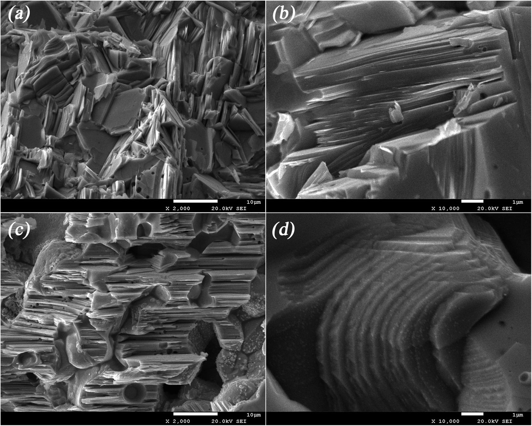 | ||
| Fig. 4 SEM images: (a) low magnification of sample 1#; (b) high magnification of sample 1#; (c) low magnification of sample 2#; (d) high magnification of sample 2#. | ||
The dependencies of the total thermal conductivity (κ) on temperature for all the samples are shown in Fig. 3(d). It first decreases and then increases as a whole over the entire temperature range. In general, κ is quite high, owing to the intrinsic metallic property of Cu2Te and the high hole concentration caused by unavoidable deviation from stoichiometry. The effects of the phase transition of Cu2Te can be noticed here as well. The first α–β transition of Cu2Te can be scrutinized from the incoherent curvature before and after 500 K. Due to the fact that both the α and β phases have hexagonal based structures, the anomalousness of this transition on κ is quite modest. Nevertheless, the β–γ transition can be easily spotted at 600 K, which implies the hexagonal to orthorhombic transformation. The following abnormality in κ at 700 K can be attributed to the orthorhombic–hexagonal (γ–δ) transition, while the higher transition temperature compared to the DSC result might be due to the thicker sample used in the thermal conductivity measurements, which may require a longer time to complete the phase transition. The last hexagonal–cubic (δ–ε) transition can be identified at around 800 K in Fig. 3(d), a few dozens of degrees higher than the DSC result due to the abovementioned reason. From Fig. 3(d) it can be seen that each of the phase transitions may induce extra phonon scattering, causing a decrease in κ. The impact of annealing time on κ can also be observed here in Fig. 3(d). Similar to that observed in Fig. 3(a) for σ, the κ of the Cu2Te bulk material experienced a decrease from the non-annealed sample to the sample annealed for 10 h, and reached a minimum value for the sample annealed for 20 h. After that, the κ of the Cu2Te bulk rose again with the annealing time prolonged to 30 h and 40 h. With the annealing time exceeding 30 h, the rise observed in both σ and κ might be related to the higher hole concentration caused by the higher degree of Cu deficiency stemming from the deviation from stoichiometry, due to the extended annealing process (Table S1†). During the experiment, we found that on the surface of the annealed samples there was some dark orange powder attached, the amount of which approximately increased with the annealing time. This powder was carefully collected and determined by XRD to be Cu (see Fig. S3†). Associated with the pores observed on the annealed samples (see Fig. 4 and S2†) and the Cu content decrease (see Table S1†), we speculated that with the increase in the annealing time, a small amount of Cu atoms escaped from the lattice and diffused to the sample surface. As a result, the longer the annealing time, the more Cu atoms escaped from the lattice, causing the deviation from stoichiometry. On the other hand, these Cu atoms aggregated on the sample surface, leaving some micro-pores in the sample.
To reveal the structural evolution contributing to the variations of thermoelectric properties, detailed microscopic investigations were carried out on the Cu2Te samples. Fig. 4 shows the fracture morphology of sample 1# and sample 2#. Fig. 4(a) and (b) illustrate the typical layered structure of Cu2Te, and the thickness of the layers ranges from tens to a few hundreds of nm. This intrinsic layered feature may endow Cu2Te with strong intralayer chemical bonds (Cu–Te covalent bonds) and very weak interlayer bonds (van der Waals forces), which have the inclination to generate a partially localized low frequency phonon mode, low sound velocity, and large phonon anharmonicity,41–43 thus leading to an enhanced thermoelectric performance. In Fig. 4(c) and (d), it can be clearly seen that there are great amounts of tiny dispersive nano-scale particles attached to the surface of each layer. According to the DSC results, it can be seen that the RT stable α-Cu2Te was absent in the cooling process, while β-Cu2Te remained until the system cooled down to RT. Thus, we speculated that these nano-scale particles might be α-Cu2Te precipitated from β-Cu2Te formed due to the non-equilibrium rapid cooling of SPS. TEM investigation was performed on sample 2# to expose in-depth information on the microstructure, as shown in Fig. 5. In Fig. 5(a), it can be seen that the typical characteristic of the submicron precipitate (∼500 nm) comprises several tinier nanocrystals of 50–100 nm in size. The inset of Fig. 5(a) shows the SAED pattern of the yellow rectangular area, in which the diffraction rings can be indexed as (100), (102), and (110) according to the interplanar distances in PDF#04-002-0652. Fig. 5(b) shows the HRTEM image of sample 2#, in which the fringe spacing was measured as 0.367 nm, corresponding to the (002) plane of Cu2Te (PDF#04-002-0652). The bright field TEM image of the nanoparticles in sample 2# is shown in Fig. 5(c) along with the EDS mapping results, which indicate the chemical composition qualitatively. The dark field STEM-EDS mapping is presented in the ESI (see Fig. S4†). Unfortunately, due to the very similar structure and identical composition of α-Cu2Te and β-Cu2Te, it is difficult to identify them quantitatively. However, further annealing would lead to an over-deviation from stoichiometry, as well as the formation of large pores (details are shown in Fig. S2 and Table S1†).
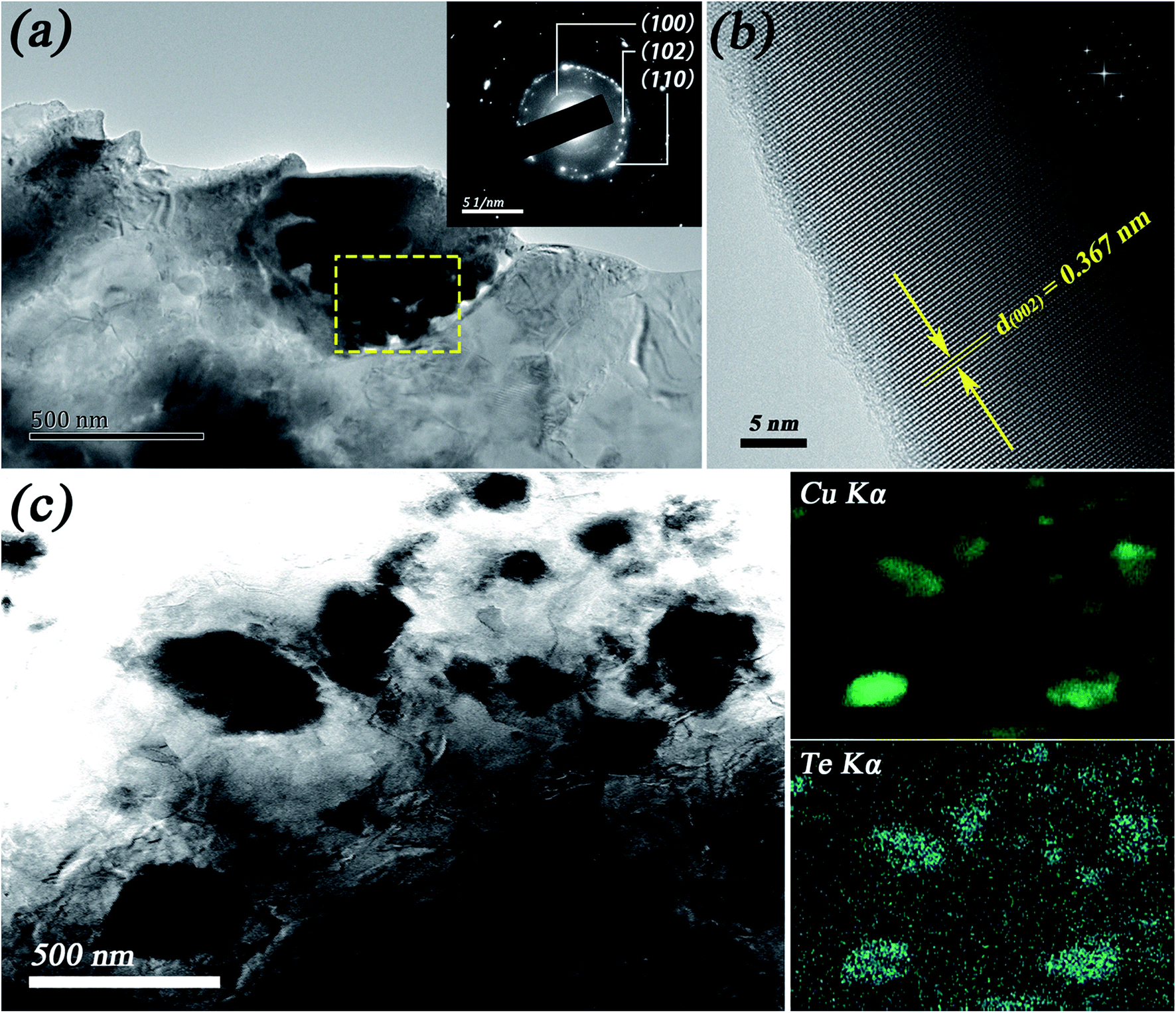 | ||
| Fig. 5 TEM images of sample 2#: (a) a Cu2Te particle comprising nanocrystals with an SAED pattern in the inset; (b) HRTEM (inset FFT); (c) BFTEM of Cu2Te particles with EDS mapping for Cu and Te. | ||
The TE figure of merit ZT is calculated based on the relevant experimental data and is shown in Fig. 6(a). The maximum PF of ∼2.7 mW K−2 m−1 was found in sample 2# at 1000 K, and combined with its κ, an optimal ZT value could approach ∼0.52 at 1000 K. Meanwhile, the ZT value at 1000 K for sample 1# was ∼0.34, and that of the other annealed samples varied from 0.29 to 0.33. The ZTs of sample 2# along with other reported Cu2Te bulk materials are shown in Fig. 6(b). It can be seen that the overall ZTs of our samples are well consistent with those reported in previous studies. However, the whole process duration in our study is much shorter than conventional ones used in previous studies, reduced from several days (a few days,37 over 10 days,18 over 7 days19) down to less than 24 hours.
 | ||
| Fig. 6 Figure of merit ZTs as a function of temperature for the Cu2Te bulk samples: (a) ZTs from 300 K to 1000 K of all samples prepared in this study; (b) ZTs of sample 2# in this study, accompanied with data from other studies for comparison. | ||
4. Conclusions
In this study, Cu2Te bulk materials were successfully prepared within 24 hours using SPS on high-energy ball-milled elemental powders in a highly efficiency way. Multiple phase transitions of Cu2Te were investigated using a combination of DSC and HTXRD. The results showed that Cu2Te experienced four successive phase transitions from room temperature to 900 K, namely α–β, β–γ, γ–δ and δ–ε, which took place at 454 K, 597 K, 627 K and 756 K, respectively. During this process, the crystal structure of Cu2Te evolved from hexagonal to orthorhombic, then back to hexagonal, and finally to cubic. This feature of Cu2Te would induce multiple critical scatterings for both charge carriers and phonons, and thus might be of great benefit for the improvement of the comprehensive thermoelectric performance. Furthermore, appropriate annealing not only can enhance the TE performance of Cu2Te, but more importantly, it can also lead to the formation of nanocrystalline particles that can serve as obstacles for the transfer of mid-wavelength acoustic phonons, as part of the all-scale hierarchical strategy to improve TE performance. An inevitable Cu deficiency could easily form in Cu2Te, creating large numbers of holes as charge carriers, leading to high electrical conductivity. However, this would also lead to a low Seebeck coefficient for the undoped Cu2Te materials. Despite the intrinsic unsatisfactory TE performance of undoped Cu2Te, it was demonstrated that the facile rapid preparation method used in this study could produce Cu2Te bulk samples with comparable ZTs to those reported in previous studies, while rapidly reducing the process duration.Acknowledgements
This work was financially supported by Tellurium & Bismuth Industrial Technology Research Institute of Sichuan Province, P. R. China.References
- G. J. Snyder and E. S. Toberer, Nat. Mater., 2008, 7, 105–114 CrossRef CAS PubMed.
- L.-D. Zhao, V. P. Dravid and M. G. Kanatzidis, Energy Environ. Sci., 2014, 7, 251–268 CAS.
- D. M. Rowe, CRC handbook of thermoelectrics, CRC press, 1995 Search PubMed.
- F. J. DiSalvo, Science, 1999, 285, 703–706 CrossRef CAS PubMed.
- M. G. Kanatzidis, Chem. Mater., 2009, 22, 648–659 CrossRef.
- B. Sales, D. Mandrus and R. K. Williams, Science, 1996, 272, 1325 CAS.
- L. Chen, X. Huang, M. Zhou, X. Shi and W. Zhang, J. Appl. Phys., 2006, 99, 064305 CrossRef.
- S. N. Girard, J. He, C. Li, S. Moses, G. Wang, C. Uher, V. P. Dravid and M. G. Kanatzidis, Nano Lett., 2010, 10, 2825–2831 CrossRef CAS PubMed.
- X. Zhou, G. Wang, L. Zhang, H. Chi, X. Su, J. Sakamoto and C. Uher, J. Mater. Chem., 2012, 22, 2958–2964 RSC.
- S. Ahmad, K. Hoang and S. Mahanti, Phys. Rev. Lett., 2006, 96, 056403 CrossRef PubMed.
- J. P. Heremans, V. Jovovic, E. S. Toberer, A. Saramat, K. Kurosaki, A. Charoenphakdee, S. Yamanaka and G. J. Snyder, Science, 2008, 321, 554–557 CrossRef CAS PubMed.
- Y. Pei, X. Shi, A. LaLonde, H. Wang, L. Chen and G. J. Snyder, Nature, 2011, 473, 66–69 CrossRef CAS PubMed.
- L.-D. Zhao, J. He, S. Hao, C.-I. Wu, T. P. Hogan, C. Wolverton, V. P. Dravid and M. G. Kanatzidis, J. Am. Chem. Soc., 2012, 134, 16327–16336 CrossRef CAS PubMed.
- L.-D. Zhao, S. Hao, S.-H. Lo, C.-I. Wu, X. Zhou, Y. Lee, H. Li, K. Biswas, T. P. Hogan and C. Uher, J. Am. Chem. Soc., 2013, 135, 7364–7370 CrossRef CAS PubMed.
- K. Biswas, J. He, I. D. Blum, C.-I. Wu, T. P. Hogan, D. N. Seidman, V. P. Dravid and M. G. Kanatzidis, Nature, 2012, 489, 414–418 CrossRef CAS PubMed.
- B. Yu, W. Liu, S. Chen, H. Wang, H. Wang, G. Chen and Z. Ren, Nano Energy, 2012, 1, 472–478 CrossRef CAS.
- H. Liu, X. Shi, F. Xu, L. Zhang, W. Zhang, L. Chen, Q. Li, C. Uher, T. Day and G. J. Snyder, Nat. Mater., 2012, 11, 422–425 CrossRef CAS PubMed.
- S. Ballikaya, H. Chi, J. R. Salvador and C. Uher, J. Mater. Chem. A, 2013, 1, 12478–12484 CAS.
- Y. He, T. Zhang, X. Shi, S.-H. Wei and L. Chen, NPG Asia Mater., 2015, 7, e210 CrossRef CAS.
- S. Butt, W. Xu, M. U. Farooq, G. K. Ren, Q. Zhang, Y. Zhu, S. U. Khan, L. Liu, M. Yu and F. Mohmed, ACS Appl. Mater. Interfaces, 2016, 8, 15196–15204 CAS.
- Y. He, P. Lu, X. Shi, F. Xu, T. Zhang, G. J. Snyder, C. Uher and L. Chen, Adv. Mater., 2015, 27, 3639–3644 CrossRef CAS PubMed.
- S. Kashida, W. Shimosaka, M. Mori and D. Yoshimura, J. Phys. Chem. Solids, 2003, 64, 2357–2363 CrossRef CAS.
- H. Liu, X. Yuan, P. Lu, X. Shi, F. Xu, Y. He, Y. Tang, S. Bai, W. Zhang and L. Chen, Adv. Mater., 2013, 25, 6607–6612 CrossRef CAS PubMed.
- B. Mansour, F. Mukhtar and G. Barakati, Phys. Status Solidi A, 1986, 95, 703–707 CrossRef CAS.
- R. Yakshibaev, N. Mukhamadeeva and R. Almukhametov, Phys. Status Solidi A, 1988, 108, 135–141 CrossRef CAS.
- N. Vouroutzis and C. Manolikas, Phys. Status Solidi A, 1989, 111, 491–497 CrossRef CAS.
- N. Vouroutzis and C. Manolikas, Phys. Status Solidi A, 1989, 115, 399–412 CrossRef CAS.
- K. Biswas, J. He, G. Wang, S.-H. Lo, C. Uher, V. P. Dravid and M. G. Kanatzidis, Energy Environ. Sci., 2011, 4, 4675–4684 CAS.
- R. J. Mehta, Y. Zhang, C. Karthik, B. Singh, R. W. Siegel, T. Borca-Tasciuc and G. Ramanath, Nat. Mater., 2012, 11, 233–240 CrossRef CAS PubMed.
- X. Tang, W. Xie, H. Li, W. Zhao, Q. Zhang and M. Niino, Appl. Phys. Lett., 2007, 90, 012102 CrossRef.
- K. F. Hsu, S. Loo, F. Guo, W. Chen, J. S. Dyck, C. Uher, T. Hogan, E. Polychroniadis and M. G. Kanatzidis, Science, 2004, 303, 818–821 CrossRef CAS PubMed.
- D. Bilc, S. Mahanti, E. Quarez, K.-F. Hsu, R. Pcionek and M. Kanatzidis, Phys. Rev. Lett., 2004, 93, 146403 CrossRef PubMed.
- P. F. Poudeu, J. D'Angelo, A. D. Downey, J. L. Short, T. P. Hogan and M. G. Kanatzidis, Angew. Chem., Int. Ed., 2006, 45, 3835–3839 CrossRef CAS PubMed.
- Y. He, T. Day, T. Zhang, H. Liu, X. Shi, L. Chen and G. J. Snyder, Adv. Mater., 2014, 26, 3974–3978 CrossRef CAS PubMed.
- Z.-H. Ge, B.-P. Zhang, Y.-X. Chen, Z.-X. Yu, Y. Liu and J.-F. Li, Chem. Commun., 2011, 47, 12697–12699 RSC.
- H. Liu, X. Shi, M. Kirkham, H. Wang, Q. Li, C. Uher, W. Zhang and L. Chen, Mater. Lett., 2013, 93, 121–124 CrossRef CAS.
- K. Kurosaki, K. Goto, A. Kosuga, H. Muta and S. Yamanaka, Mater. Trans., 2006, 47, 1432–1435 CrossRef CAS.
- D. Salmon and R. Tye, Int. J. Thermophys., 2010, 31, 338–354 CrossRef CAS.
- D. Salmon, R. Brandt and R. Tye, Int. J. Thermophys., 2010, 31, 355–373 CrossRef CAS.
- Y. Zhang, B. Sa, J. Zhou and Z. Sun, Comput. Mater. Sci., 2014, 81, 163–169 CrossRef CAS.
- D. Yang, W. Yao, Q. Chen, K. Peng, P. Jiang, X. Lu, C. Uher, T. Yang, G. Wang and X. Zhou, Chem. Mater., 2016, 28, 1611–1615 CrossRef CAS.
- L. Wu, J. Yang, S. Wang, P. Wei, J. Yang, W. Zhang and L. Chen, Phys. Rev. B: Condens. Matter Mater. Phys., 2014, 90, 195210 CrossRef.
- Y. Zhang, X. Ke, P. R. Kent, J. Yang and C. Chen, Phys. Rev. Lett., 2011, 107, 175503 CrossRef PubMed.
Footnote |
| † Electronic supplementary information (ESI) available. See DOI: 10.1039/c7ra02145c |
| This journal is © The Royal Society of Chemistry 2017 |