
 Open Access Article
 This Open Access Article is licensed under a Creative Commons Attribution-Non Commercial 3.0 Unported Licence
Influence of O2, H2O and airborne hydrocarbons on the properties of selected 2D materials
Zhenbo Peng†
ac,
Rui Yang†
bc,
Min A. Kim†
 c,
Lei Li
*de and
Haitao Liu
*c
c,
Lei Li
*de and
Haitao Liu
*c
aChemical Engineering College, Ningbo Polytechnic, 1069 Xinda Road, Economical & Technical Development Zone, Ningbo, 315800, P. R. China
bDepartment of Chemistry, Beihua University, Jilin, 132013, P. R. China
cDepartment of Chemistry, University of Pittsburgh, Pittsburgh, Pennsylvania 15260, USA. E-mail: hliu@pitt.edu
dDepartment of Chemical & Petroleum Engineering, Swanson School of Engineering, University of Pittsburgh, Pittsburgh, Pennsylvania 15261, USA. E-mail: lel55@pitt.edu
eDepartment of Mechanical Engineering & Materials Science, Swanson School of Engineering, University of Pittsburgh, Pittsburgh, Pennsylvania 15261, USA
First published on 22nd May 2017
Abstract
This paper reviews the effect of ambient exposure on the properties of selected 2D materials. Many molecules in ambient air can adsorb onto 2D material surfaces to impact their properties and device performance. This paper highlights recent work on the interaction between 2D materials and three ambient-present molecules: O2, H2O, and airborne hydrocarbons. We focus our discussions on graphene but also include research on other 2D materials, such as BN, transition metal dichalcogenides, and 2D heterostructures. We discuss the molecular mechanism of their interactions with 2D materials and the impact on electrical, optical, and wetting properties and device performances.
 Zhenbo Peng | Zhenbo Peng received his B.S. in chemistry and M.S. in analytical chemistry from University of Science and Technology of China (Hefei, China). He obtained his PhD in material physics and chemistry at Ningbo Institute of Technology and Engineering, Chinese Academy of Sciences in 2013. He is now an associate professor in Ningbo Polytechnic and was a visiting scholar at the University of Pittsburgh. His research interests include the surface properties and the reactivity of graphene and other 2D materials. |
 Rui Yang | Rui Yang received his B.S. in chemistry from Jilin Normal College and his M.S. from Northeast Normal University. He joined the college of chemistry and biology of Beihua University in 1999 and is currently an associate professor there. His research interests include functionalization of graphene, synthesis of nanomaterials and their applications in catalysis. |
 Min A. Kim | Min A Kim received her B.S. in chemistry and B.S. in mathematics from La Roche College (Pittsburgh, PA) in 2013. She then worked as an adjunct in the faculty of mathematics at La Roche College. Since 2014, she has been a Ph.D. student in the chemistry department of the University of Pittsburgh, in the group of Prof. Haitao Liu. Her research interests include the surface properties and the reactivity of graphene and other 2D materials. |
 Lei Li | Lei Li received his B.S. and M.S. in polymer material from Tsinghua University (Beijing, China) in 1994 and 1997. He received his Ph.D. in macromolecular science & engineering from the University of Michigan in 2001, under the guidance of Professor Albert Yee. He joined Seagate Technology LLC in 2001. In 2010, he join the department of chemical & petroleum engineering of the University of Pittsburgh, where he is now an associate professor. His research interests include surface, interface and 2D materials. |
 Haitao Liu | Haitao Liu received his B.S. in chemistry and computer science from the University of Science and Technology of China (Hefei, China) and his Ph.D. in chemistry in 2007 from the University of California, Berkeley. He carried out postdoctoral research at Columbia University before joining the chemistry department of the University of Pittsburgh, where he is now an associate professor. His research interests include DNA-based nanofabrication, surface properties of graphitic materials, and reaction mechanism of the synthesis of inorganic colloidal nanocrystals. |
1 Background
2D materials include (semi)metals, semiconductors, and insulators. They have been used in a wide range of applications such as electrochemistry, electronics, and optoelectronics. All atoms of 2D materials are on or near the surface. The nanoscale thinness of 2D materials is key to many of their applications, such as the vertical tunnelling field effect transistors (FETs),1 and electrically tunable optical absorbers.2 For the same reason, many properties of 2D materials will change upon surface adsorption of molecules present in the ambient; in many cases, such processes will negatively impact the material performance and contribute to inconsistency and irreproducibility of the experimental results. Therefore, it is important to understand and control the environmental impact in order to achieve the full potential of 2D materials. These issues are receiving increasing attentions, in part due to the need to improve performance, consistency, and reproducibility of devices fabricated from 2D materials.This paper reviews the effect of ambient environments on the properties of 2D materials, focusing on three molecules: O2, H2O, and airborne hydrocarbons. We highlight the molecular picture of the interfacial processes and their implication to the electronic, optical, and wetting properties of 2D materials. Graphene is the most studied material system in this regard and will be the focus of this review. Other 2D materials, including BN, transition metal dichalcogenides, and 2D heterostructures, will be discussed when appropriate. Due to space constrain, we will limit the discussion to studies conducted at or close to room temperature and will not cover high temperature studies (e.g., oxidation) of 2D materials.
Water and oxygen are the most recognized environmental factor impacting properties of 2D materials. Both molecules physisorb and chemisorb onto many 2D materials and their effect was known since the research on carbon nanotubes. Recently, it was shown that high molecular weight hydrocarbon is another contaminant that can strongly adsorb onto 2D materials. Although the concentration of hydrocarbon in air (<ppm) is several orders of magnitude lower than that of O2 and H2O, 2D materials surfaces can still be contaminated by hydrocarbons within seconds to hours because of their fast diffusion in air.
2 O2: p type charge doping
2.1 Charge doping of graphene
Molecular oxygen can adsorb onto graphene to result in hole doping. This effect is similar to that observed on carbon nanotubes, in which case it was suggested that endoperoxide (i.e., chemical adsorption) is formed on the curved carbon surface as a result of O2 adsorption.3,4 Compared to carbon nanotubes, graphene has two significant differences: the absence of the high curvature and the 2D geometry. The former makes the formation of endoperoxide not energetically feasible while the latter makes it possible to trap molecules, including O2 between graphene and a supporting substrate. As a result, the mechanism of O2-induced charge doping of graphene could be different from that of the carbon nanotubes. There has been extensive work to understand the interaction between O2 and graphene. However, detailed molecular picture of the adsorption and charge doping has not been well understood, in part due to the difficulty to characterize the chemical nature of adsorbed oxygen species. Many surface sensitive spectroscopy techniques require ultra-high vacuum, which lead to the desorption of O2 from the surface.Ryu et al. reported a very detailed study of the charge doping of exfoliated graphene by O2 using Raman spectroscopy, in which case the doping level of graphene can be extracted from the Raman G peak position and linewidth.5 They found that the level of hole doping by O2 is affected by two factors: the presence of water vapor and the mechanical coupling between graphene and the substrate. The effect of water is illustrated in Fig. 1a, where the G band position was measured on an exfoliated graphene as a function of various processing conditions. The G peak position shifted to higher wavenumber upon exposure to dry O2 and shifted back upon flowing dry Ar (black and blue dots). This data suggests that O2 reversibly hole dopes graphene (hole density ca. 4 × 10¹²/cm2), which is also confirmed by field effect measurement. No noticeable shift in the Raman peak position was observed when the sample was exposed to wet N2 (green dots). However, the presence of both H2O and O2 caused a much larger shift in the G peak compared to the case of flowing O2 alone, which is only partially restored by flowing dry Ar. This result shows that although water itself does not significantly dope graphene, it does assist the hole-doping of graphene by O2. The effect of graphene–substrate interaction is shown by comparing supported and suspected graphene (Fig. 1b). The supported graphene produced a large increase in the Raman G peak after annealing while the suspended portion showed a much smaller change. It should be noted that strain can change the Raman peak features as well. In a recent study, Lee et al. reported a Raman-based approach to separate the effect of strain and charge doping and showed that heating graphene to 150 °C is sufficient to activate the O2 induced hole doping.6
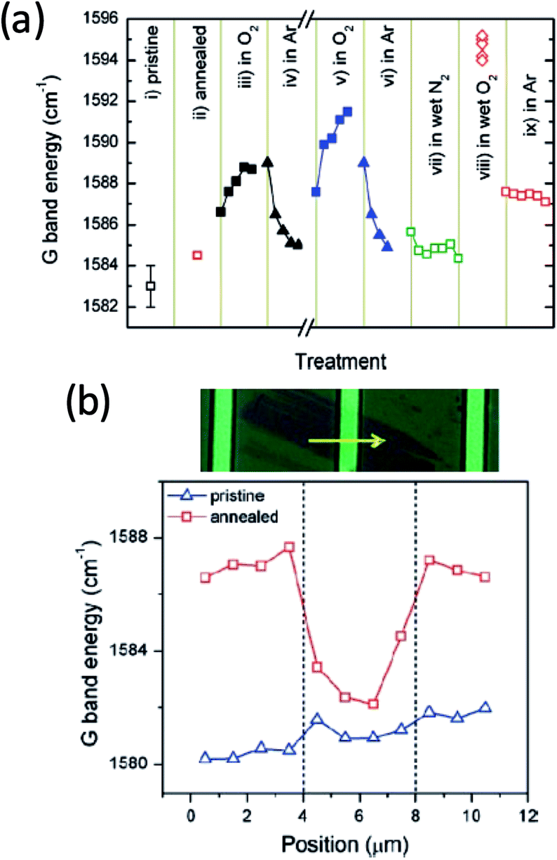 | ||
| Fig. 1 (a) Effect of thermal treatment and O2 on the Raman G peak shift of an exfoliated graphene sample. Higher G peak position is correlated with higher p doping in this case. (b) A linear scan of Raman G peak shift of an exfoliated graphene. As shown in the micrograph, the middle portion of this graphene sample was suspended over a trench that is ca. 4 μm in width (between 4–8 μm in the line scan). Reproduced with permission from Ryu, S.; et al., Nano Lett., 2010, 10, 4944. Copyright American Chemical Society. | ||
Sato et al. studied O2 adsorption on bilayer graphene using field effect measurements.7 In their work, a field effect transistor was fabricated using an exfoliated bilayer graphene sample and exposed to O2; its transfer characteristics (i.e., source–drain current as a function of back gate voltage) was used to quantify the degree of charge doping induced by O2 adsorption. The shift of charge neutrality point in their FET measurement directly correlates with the degree of charge doping. The most interesting finding of their work is that the degree of O2-induced hole doping is a function of not only time but also the gate voltage. Specifically, positive gate voltage (i.e., electrically electron-doped graphene) promotes the O2 adsorption and negative gate voltage inhibits it (Fig. 2). In other studies, oxygen has been suggested to play a role in the hysteresis behavior of graphene FETs. Although water was believed to be the major contributing factor (see Section 3), the gate hysteresis of graphene FETs was observed even with a very short time of pulsed Vg in dry oxygen environment.8 Yang et al. suggested that the charge transfer between graphene and O2 leads to a negatively charged adsorbate layer on the surface of graphene.8
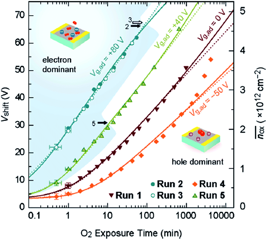 | ||
| Fig. 2 Effect of gate voltage on the time dependence of O2-induced charge doping of bilayer graphene. The charge doping level is calculated using the shift of the charge neutrality point (Vshift). Reproduced with permission from Satu, et al., Nano Lett., 2011, 11, 3468. Copyright American Chemical Society. | ||
The molecular mechanism of O2 adsorption and charge doping has been under intense investigation. However, definitive conclusion has not been made due to challenges in characterizing the molecular and bonding structure of the adsorbed oxygen species. The covalent bonding of O2 onto the basal plane of graphene, in the form of epoxide or endoperoxide, is not likely due to the absence of D peak in the Raman spectrum.5 The most widely accepted model is that charge doping is mediated through an electrochemical mechanism, in which O2 is reduced by electron transfer from graphene and the reduction products (e.g., OH−) are stabilized by the substrate (e.g., SiO2) and adsorbed water. This adsorption mode involves chemical transformation (i.e., similar to chemisorption), yet at the same time it is reversible and does not produce chemical defects on graphene (i.e., similar to physisorption). The variations in the doping within and between graphene samples can be explained by trapped O2 and H2O between graphene and substrate. It was shown that water can diffuse between graphene and SiO2, forming a water layer of ca. 3.5 Å thickness.9 The intercalation of water significantly reduced the hole-doping of graphene, supporting the idea that the O2-induced hole-doping is due to trapped species underneath graphene and/or interaction between SiO2 and graphene. This mechanism also explains the effect of gate voltage on the adsorption of O2: if one assumes that the electron transfer is the rate limiting step of O2 adsorption, then such process should be dependent on the electrochemical potential of graphene.7 Specifically, increasing the potential (i.e., electron doping) of graphene should increase the adsorption rate and reducing the potential (i.e., hole doping) should decrease the rate, as has been shown by the data in Fig. 2.
2.2 O2 adsorption on transition metal dichalcogenides (TMDs)
Gao et al. reported that MoS2 and WS2 showed significant crack and quenching of PL after storage in air for several months, which the authors attributed to oxidation by O2 and H2O.10 Oxygen adsorption significantly impacts the operation of MoS2 FET devices.10 Qiu et al. observed significant increase of the on-state current in high vacuum compare to air on bi-layer MoS2 FETs, which is an n-type device. Vacuum annealing at 350 K resulted in a further increase of on-state current while exposure to dry oxygen decreased the on-state current by as much as 100 times.11 The surface oxygen-containing species, as determined by X-ray photoelectron spectroscopy (XPS), showed a 43% reduction when an air-exposed sample was annealed in UHV at 350 K for 24 hours. This 43% of oxygen-containing species are likely physisorbed given the low desorption temperature. These results suggest that hole doping by O2 reduces the carrier density in MoS2 and consequently decreases the on-state current.11 Yue et al. studied the adsorption of various gases on MoS2 by density functional theory calculation and found that both O2 and H2O act as electron acceptors while NH3 is an electron donor.12The optical properties of monolayer TMDs can be also greatly affected by O2. Tongay et al. demonstrated the modulation of the photoluminescence (PL) intensity of monolayer TMDs by O2 and H2O (Fig. 3).13 They showed that the vacuum annealing process greatly enhanced PL intensity by thermally desorbing initial contaminants and organic residues from the surfaces of TMDs. After the vacuum annealing, the PL intensity of monolayer MoS2 became extremely sensitive to O2 and H2O environments. Inert gases such as Ar and N2 did not affect the PL intensity, and the change in PL intensity by O2/H2O was completely reversible, again indicating physisorbed nature for these species. The PL intensity response was almost instantaneous and proportional to the O2 or H2O pressure.13 Moreover, the enhancement of PL intensity was more significant when MoS2 was exposed to ambient condition (O2 and H2O together) compare to the individual exposure of O2 and H2O, again suggesting electrochemical p-doping by O2 is at play.13 It was suggested that p doping by O2 reduces the charge carrier density, which could destabilize exciton by forming trion and therefore reduces PL intensity. It is interesting to note that WSe2, a p type semiconductor, showed the opposite behavior from MoS2, i.e., O2 exposure reduces the PL intensity. This observation can be again explained by the effect of p doping by O2, which increases the major charge carrier density in WSe2 and reduces PL intensity by forming trion. In a more recent study, Nan et al. reported significant PL enhancement on defected area of MoS2 after the sample is annealed at high temperature, which was explained by the same mechanism.14
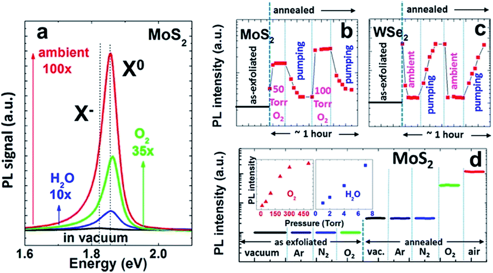 | ||
| Fig. 3 Effects of different gas environments on the PL intensity of annealed monolayer TMDs. (a) Change in PL intensity on MoS2 in H2O, O2, and ambient (H2O and O2) environments. Trion X− and exciton X0 peak positions are indicated. Modulation of the PL intensity of (b) monolayer MoS2 with O2 exposure (50 and 100 Torr), and (c) monolayer WSe2 with ambient air (760 Torr). The opposite response was observed in MoS2 (n-type) and WSe2 (p-type). (d) Effect of Ar, N2, O2, and air on the PL intensity of as-exfoliated and vacuum annealed monolayer MoS2. Inset: PL intensity as a function of O2 and H2O pressure. The PL intensities in panels (b)–(d) are log scale. Adapted with permission from Tongay, S. et al., Nano Lett., 2013, 13, 2831–2836. Copyright American Chemical Society. | ||
The effect of air on the photocurrent of the MoS2 monolayer was also reported. Zhang et al. measured the source–drain current at fixed source–drain and gate voltages under various illumination light power density (λ = 532 nm), and observed much larger photocurrent decay in vacuum compare to ambient air environment.15 Another study reported similar result using deep ultraviolet light (λ = 220 nm) excitation in N2 and O2 gas environments.16
3 H2O: gating hysteresis
Water can physisorb onto both 2D materials and their supporting substrates. Being an impermeable membrane, 2D materials can effectively trap water between itself and the substrate.17 The electrical measurements of 2D-material-based FETs often show large hysteresis in the transfer characteristics (i.e., source–drain current vs. gate voltage).18–25 It is commonly agreed that water is a major contributor to the hysteresis although the exact mechanism is still under investigation. It should be noted that chemisorption of water on 2D materials has also been extensively studied, although it will not be reviewed here. For example, water (but not O2, H2, or NH3) can react with line defects within Ru(0001)- and Cu(111)-supported graphene to result in physically damage of the film.263.1 Graphene FETs
Lohmann et al. studied the gate hysteresis in ambient conditions using FETs fabricated on mechanically exfoliated graphene.27 As shown in Fig. 4, subjecting the FET to positive (negative) gate voltage (Vbg or Vg) moved the charge neutrality point to the same direction, indicating that graphene is more hole (electron) doped as a result of the gating history. Both low Vg sweeping rates and large Vg scan range enhanced the shift in charge neutrality point. When graphene FETs were kept under vacuum (3 × 10⁻⁵ mbar) for several hours, significant shift of charge neutrality point toward zero Vbg occurred, suggesting gradual desorption of hole doping adsorbates, presumably O2. The hysteresis behavior was also diminished in vacuum.27 Analogous to the hysteresis observed with carbon nanotube FETs,28 it was proposed that water molecules adsorbed on the graphene or SiO2 surface in ambient condition, and the hysteresis was attributed to the charge trapping mediated by water molecules and the migration of the mobile ions (e.g., Na+) in the SiO2 substrate (Fig. 5).29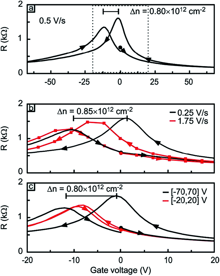 | ||
| Fig. 4 Gate hysteresis of graphene FETs. (a) Vg sweep started from 0 V (black dot) to +70 V to −70 V to 0 V. The arrows indicate the sweep direction. (b) Change in gate hysteresis with two different Vg scan rate. Vg interval was ±70 V (c) the change in gate hysteresis with two different Vg interval. The scan rate of 0.5 V s−1 was used. Adapted from Lohmann, T. et al., Nano Lett., 2009, 9, 1973–1979. Copyright American Chemical Society. | ||
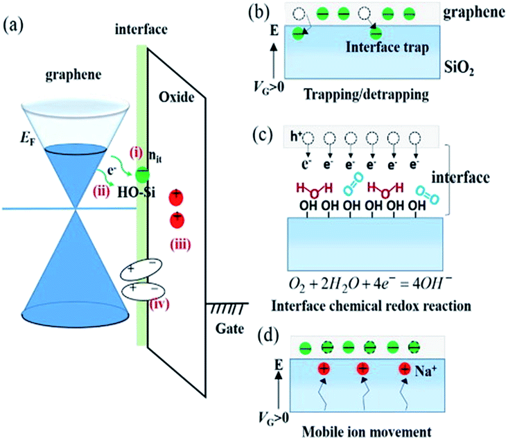 | ||
| Fig. 5 Proposed mechanisms of hysteresis of graphene FET. (a) Energy diagram of FET device. (b) Charge trapping at the surface of SiO2. (c) Redox reaction between graphene and trapped H2O/O2. (d) Mobile ion mechanism. Reproduced with permission from Feng, T.; et al., Carbon, 2014, 78, 250. Copyright Elsevier. | ||
The electrochemical O2/H2O redox couple was also suggested as a possible mechanism for the hysteresis observed in FET devices (Fig. 5b). Veligura et al. measured the transfer characteristics of graphene FET as a function of relative humidity.25 They observed that short exposure to water vapor did not produce hysteresis while high humidity levels did. In addition, ethanol vapor did not induce hysteretic behavior nor doping effect on graphene FETs. Given the similar dipole moment of ethanol and water, 1.68 D and 1.85 D, respectively, the result shows that the polar nature of water molecules was not a significant factor in the observed hysteresis.25 They proposed that the O2/H2O redox reaction could change the local pH and was responsible for the hysteresis. Similar claims were also made by Xu et al.30 Assuming surface-adsorbed water is in equilibrium with air (pH = ca. 6), the Fermi level of undoped graphene (−4.6 eV)31 lies above the electrochemical potential of the solution (−5.3 eV relative to vacuum level). Hence, electrons can transfer from graphene to O2 solvated in the adsorbed water layer, resulting in hole doping of graphene in air. Back gating will change the initial electrochemical equilibrium between graphene and the O2/H2O redox couple, and the charge transfer occurs continuously under the sweeping of Vg to establish a new equilibrium.30 Feng et al. reported the temperature dependence of the hysteresis in ambient condition.32 They observed a shift of charge neutrality point toward 0 V as the temperature was increased from 300 K to 380 K,32 which is consistent with the desorption of hole doping molecules (Fig. 6a). The hysteresis also increased upon heating (Fig. 6b) and this observation is consistent with charge trapping, O2/H2O redox, and mobile ion mechanisms.32 In contrast, Joshi et al. observed that the transconductance hysteresis persisted even after vacuum annealing at 200 °C for ∼20 h; they also estimated the density of water-related electron traps to be ∼2.4 × 1010 cm−2 eV−1.18 On the other hand, Wang et al. reported that at low temperature (<0 °C), the hysteresis changes its direction, i.e., subjecting the FET device to positive gate voltage decreases the charge neutrality point.20 It was proposed that the strong dipole of an ice layer on graphene was responsible for the effect. Similar observations was also made by Liao et al., who reported the reversion of the hysteresis behaviour at ∼215 K and proposed that the frozen electron-trap states of H2O can be turned into the hole-trapping states as the temperature decreases, thus result in the reversion of the hysteresis.19
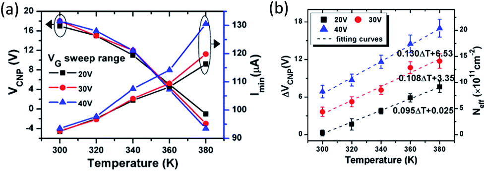 | ||
| Fig. 6 Temperature dependence of (a) charge neutrality point and (b) shift in charge neutrality point of a graphene FET. Adopted with permission from Feng, T.; et al., Carbon, 2014, 78, 250. Copyright Elsevier. | ||
Consistent with the water-assisted mechanism, the hysteresis can be suppressed by the surface treatment of the substrate. For example, by applying phenyl-terminated organosilane self-assembled monolayer onto the dielectric surface, improvement in mobility, hysteresis, and bias stress stability of graphene FETs were observed.33 Many other passivation layer on the dielectric surface were also used, such as poly(methyl methacrylate) (PMMA),27 parylene,34 and hexamethyldisilazane (HMDS).18
3.2 MoS2 FETs
Similar to the case of graphene, single layer MoS2 FETs also exhibit hysteresis behaviour in ambient conditions. Late et al. showed that the threshold gate hysteresis steadily increased with increased relative humidity, and vacuum and dry air environments both reduced hysteresis behavior. These results suggest that adsorbed water molecules is responsible for the hysteretic behavior.35 Interestingly, keeping the device in the dark suppresses the threshold gate hysteresis in comparison to white illumination (radiant flux density ∼0.7 mW cm−2).35 As the illumination was turned off, charge carrier concentration decreases and the charge transfer can be suppressed. Suppression of the hysteresis was further demonstrated by protective coating of MoS2 FETs with amorphous Si3N4. In contrast to graphene FETs, the threshold gate hysteresis observed in vacuum was not negligible and also observed with suspended MoS2 FETs in vacuum, suggesting additional mechanisms, possibly intrinsic to the MoS2 material itself, is at play.364 Airborne hydrocarbons
There is a rich literature of airborne hydrocarbon adsorption on high energy surfaces, such as metals and ceramics. All high energy surfaces get contaminated by airborne hydrocarbon contamination.37 In fact, adventitious carbon peak has been used as a binding energy reference for XPS spectrum.38,39 What has not been widely recognized is that many low energy surfaces, such as graphene and other 2D materials, also adsorb airborne hydrocarbon when exposed to air and such adsorption significantly changes their surface properties.4.1 Wetting transition of graphene
Early studies by Schrader investigated contamination of graphite by ultra-high vacuum (UHV) surface science techniques and water contact angle measurement.40,41 It was reported that graphite surface cleaned in UHV showed a lowed water contact angle (i.e., more polar) than that prepared in air and it was suggested that surface contamination is responsible for this effect.40 However, spectroscopic evidence of hydrocarbon contamination was not presented in that study and the community still overwhelmingly accepted that graphite is a hydrophobic material.Airborne hydrocarbon contamination of graphene was systematically studied by a number of recent studies. Li et al. reported that the water contact angle of a freshly prepared chemical vapor deposition (CVD)-grown graphene (supported on a Cu foil) is about 42°, significantly lower than the commonly accepted value of 90°. It was shown that airborne hydrocarbons adsorb onto graphene surface within minutes to hours and the surface becomes hydrophobic as a result.42 Using graphite as a model, Kozbial et al. showed that the surface accumulates ca. 0.5 nm thick of hydrocarbon from air, which is responsible for a wetting transition from ca. 64° (freshly cleaved sample) to ca. 80° (air-aged sample, Fig. 7).43 Attenuated total refection (ATR) FTIR and XPS data suggest the presence of hydrocarbon on the surface, which can be removed by high temperature annealing and UV/O3 treatment.42 These results are reproduced by a number of parallel and follow-up studies using supported and partially suspended graphene as well as graphite.44–51 In particular, Ondarçuhu et al. measured water contact angle on partially suspended graphene and concluded that a totally suspended graphene should have a water contact angle of 85° ± 5°.52 In a more recent work, Kozbial et al. also used dynamic contact angle measurements to assess the role of defects in the wettability of freshly exfoliated graphite.53 They argued that the advancing contact angle reflects the wettability of defect free graphite while the density of defects in graphite determines its receding contact angle. They reported an advancing WCA for pristine graphite to be 68.6°, which indicates that graphitic carbon is intrinsically mildly hydrophilic. Note that the contact angle of graphitic materials significantly depends on their supporting substrate. This phenomenon, termed (partial) wetting transparency,42,54,55 is the reason behind the large variation of contact angles reported for Cu-supported graphene (42°), suspended graphene (85°), and graphite (64–68.6°).
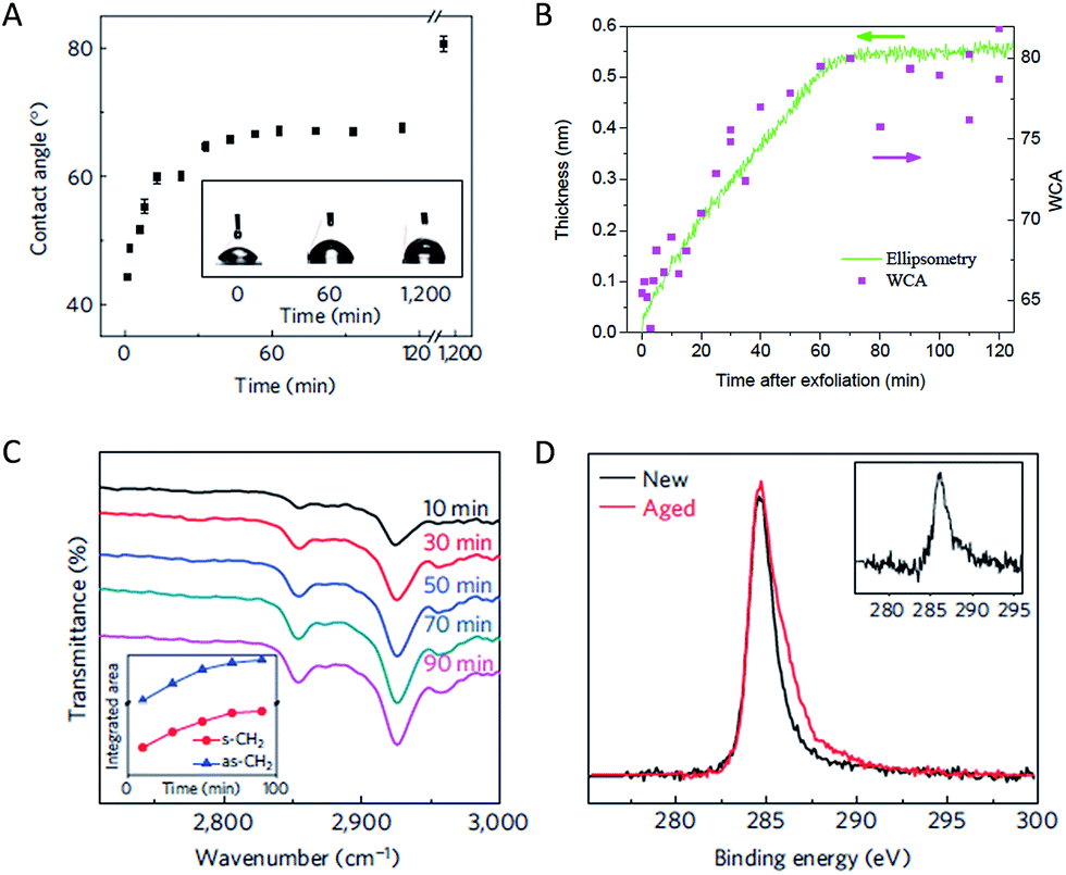 | ||
| Fig. 7 Adsorption of airborne hydrocarbon onto graphitic surfaces. (A) Hydrophilic-to-hydrophobic wetting transition of a copper-supported graphene sample in air. The inset shows selected contact angle (WCA) data. (B) High correlation between wettability and thickness of adsorbed hydrocarbon for an exfoliated HOPG sample in air. (C) C–H vibration region of ATR-FTIR spectra that were collected from a copper-supported graphene sample exposed to air. The inset shows the intensity of the symmetrical (s) and anti-symmetrical stretching (as) peaks of –CH2– as a function of time. (D) Effect of aging in air (several days) on the carbon XPS peak of a copper-supported graphene. The inset shows the difference spectrum. Panel (A) (C) (D) are adapted with permission from Li et al., Nature Mater., 2013, 12, 925. Copyright Nature Publishing Group. Panel (B) is adapted with permission from Kozbial, et al., Carbon, 2014, 74, 218. Copyright Elsevier. | ||
Wettability of a surface is directly linked to its surface free energy. Kozbial et al. showed that the surface energy (Fowkes model) of a clean copper-supported graphene is ca. 25% higher than that of a contaminated sample.56 A surprising finding of their work is that the surface energy of clean graphene and graphite contains a significant polar contribution. This result contrast with the traditional view that graphitic materials are non-polar. The origin of such polar contribution is not clear but could originate from π-hydrogen bonding interactions and charge doping by the substrate.
It should be noted that none of the recent studies have verified the surface cleanness of their samples. Instead, the change of contact angle was used as an indication that the surface is getting contaminated and that the freshly prepared surface is assumed to be reasonably clean. The reported contact angle values and kinetics showed some variations, which is expected as the type and concentration of airborne hydrocarbon will depend on the location. It will be very interesting to measure water contact angle on a surface verified to be clean, as in the work of Schrader, while at the same time, address the water evaporation issue in that work.40,41 Within this context, it is worth noting that many plastics emits hydrocarbon and as a result, glovebox and cleanroom should not be assumed to be hydrocarbon-free.42,57,58
The interaction between the hydrocarbon and the graphitic carbon substrates are likely physisorption in nature. The adsorbed species can be removed by a thermal annealing in vacuum without introducing significant defects into the carbon materials.42,43 The weak binding of the contaminant poses significant challenges in their structural characterization. Traditional surface science techniques, such as XPS and transmission electron microscopy, rely on ultra-high vacuum, which inevitably results in a partial or complete desorption of the contaminant. Fortunately, significant efforts have been made to adopt these techniques for ambient pressure analysis (e.g., ambient pressure XPS).59 FTIR has been extensively used in the recent literature as it has the needed sub-monolayer sensitivity and chemical specificity.42–44,46 Tip-enhanced FTIR is a particular interesting tool because it provides the much needed spatial resolution.60 Other characterization tools has also been used to characterize the surface, such as ellipsometry and force measurement.43,44,46 Unfortunately, these methods do not provide the structural information of the contaminant.
4.2 Effect on electrochemistry of graphene
The presence of hydrocarbon significantly decreases the rate of electron transfer from a graphene electrode to solution redox couples. It was long believed that the basal plane of graphene and graphite has very low electrochemical activity compared to metal electrodes, due to their low density of state and absence of adsorption of redox couples. It is now understood that such low activity is, at least in part, due to surface contamination by hydrocarbons.47,61,62 Several research groups, in particular Unwin, Dryfe, and Amemiya have shown that the electrochemical activity of graphite and graphene is sensitive to air exposure and suggested that hydrocarbon contamination lead to a decrease of electrode performance (Fig. 8a).47,57,61–65 These data suggests that airborne hydrocarbon contamination on graphene persists in water. The Amemiya group also showed that by partially reducing hydrocarbon contamination on the surface, the electrochemical activity of graphene and graphite can be drastically improved.47,61,65 In one study, they used scanning electrochemical microscopy-based nanogap voltammetry method to measure the heterogeneous electron transfer rate constant on a highly oriented pyrolytic graphite (HOPG) electrode. During the electrode fabrication process, the HOPG surface was protected from airborne hydrocarbon contamination using a water adlayer.66 Their study reported extremely high rate constants (≥12 cm s−1) that are many orders of magnitude higher than previous believed possible for HOPG (Fig. 8b).67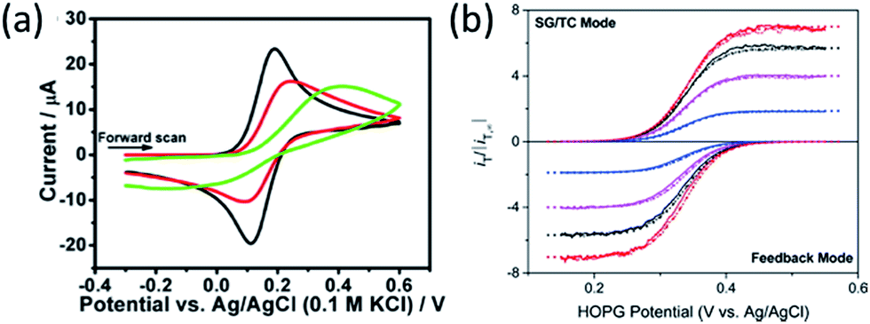 | ||
| Fig. 8 (a) Effect of air exposure on the electrode activity. The cyclic voltammetry was collected using a freshly cleaved HOPG electrode; the electrolyte was 1 mM Fe(CN)64− in 0.1 M KCl. The HOPG was left in air for 0 min (black), 1 h (red), and 3 h (green). Reproduced with permission from Patel, A. N.; et al., J. Am. Chem. Soc., 2012, 134, 20117. (b) Nanogap voltammograms collected on an HOPG surface with reduced hydrocarbon contamination. The electrolyte was 0.3 mM of (ferrocenylmethyl)trimethylammonium in 50 mM KCl. Reproduced with permission from Chen, R.; et al., Anal. Chem., 2016, 88, 8323. Copyright American Chemical Society. | ||
4.3 Airborne hydrocarbon contamination of other 2D materials
Several other 2D materials, including WS2, MoS2, and BN, also undergo the same hydrocarbon contamination when exposed to ambient air. Chow et al. prepared WS2 samples on SiO2 and reported that the freshly prepared sample showed an advancing water contact angle of ca. 70° and for air-aged sample the value increases to ca. 83°.68 Similarly, Kozbial et al. showed that freshly exfoliated MoS2 has a water contact angle of 69° that increases to 89° after 1 day of exposure in air.69 Hydrocarbon contamination was proposed to be responsible for the superhydrophobic behavior of BN nanotubes.70 Li et al. studied the hydrocarbon adsorption on single layer BN grown on Cu, Ge, and Ni substrates. In all the three cases, they observed an increase of water contact angle (from ca. 63° to ca. 86°) as the freshly prepared sample ages in air. In a related study, Annamalai et al. reported wettability of a number of van der Waals heterostructures (e.g., WS2/BN, graphene/BN, MoS2/WS2).71 Their data was taken on thermally annealed samples and the result suggests contribution from the sub-layer to the wettability, i.e., partial wetting transparency.54,55The contamination does not noticeably impact the AFM imaging of the 2D material in the topography mode although it does change its surface potential.51 The hydrocarbon contaminant form nanoscale bubbles when two pieces of 2D material are stacked together to create a van der Waals heterostructure.72 These experimental evidence suggest that the adsorbed hydrocarbons behave like a liquid on the surface of 2D materials. Many of the applications of van der Waals heterostructures rely on their atomic cleanness and therefore, it will be important to understand and control their surface contamination by airborne hydrocarbons.1,73,74
5 Conclusion and outlook
Due to their unique geometry, the properties of 2D materials can be significantly impacted by adsorption of molecules from ambient environment. Understanding and controlling such environmental factors played a key role in revealing the true nature of 2D materials, such as the extreme charge mobility and high electrochemical activity of graphene, and the true surface energy of 2D materials. Within this context, the effect of O2 and H2O are now widely appreciated. In contrast, airborne hydrocarbon has not received as much attention, in part due their low concentration in air. However, as we showed, airborne hydrocarbon contamination of many 2D materials is fast and their impact on the wetting and electrochemical properties is enormous.Looking forward, it remains a challenge to fully understand the interaction between ambient-present molecules and 2D materials at the molecular level. For example, the mechanism for the O2-induced charge doping still lacks definitive experimental support; the chemical nature of the hydrocarbon contaminant is yet to be fully characterized. Addressing these fundamental questions is a key component in understanding the intrinsic properties of 2D materials and improving their performances in various devices. A major technical challenge in these studies is the lack of spectroscopic tools that can probe the 2D material surface with high surface sensitivity and spatial resolution at ambient environment. The rapid development of ambient pressure XPS, environmental TEM, and AFM-FTIR may provide the much-needed help in these cases.59,60,75 For studies of hydrocarbon contamination, another challenge is the availability of a hydrocarbon-free ambient environment. The 2D materials are sensitive to even parts-per-trillion level of hydrocarbon vapor. Maintaining such a low hydrocarbon concentration in ambient pressure, which is required for wetting and electrochemical studies, requires special purification of air and solvents as well as eliminating hydrocarbon emission sources (e.g., plastic tubing, oil pump) in the experimental setup.
Despite these challenges, exploring the interactions between ambient molecules with 2D materials will be extremely rewarding. At the bare minimum, the learnings are key to improve the reproducibility of devices (e.g., FETs), and material properties (e.g., PL, wettability). In the case of graphitic materials, the recent studies have already revealed clean graphene/graphite as completely different from their ‘dirty’ counterparts.76 Exploiting these new material properties will lead to new applications and device concepts.
Acknowledgements
HL acknowledges partial support from ONR (N000141512520).References
- L. Britnell, R. V. Gorbachev, R. Jalil, B. D. Belle, F. Schedin, A. Mishchenko, T. Georgiou, M. I. Katsnelson, L. Eaves, S. V. Morozov, N. M. R. Peres, J. Leist, A. K. Geim, K. S. Novoselov and L. A. Ponomarenko, Science, 2012, 335, 947 CrossRef CAS PubMed.
- M. Liu, X. B. Yin, E. Ulin-Avila, B. S. Geng, T. Zentgraf, L. Ju, F. Wang and X. Zhang, Nature, 2011, 474, 64 CrossRef CAS PubMed.
- P. G. Collins, K. Bradley, M. Ishigami and A. Zettl, Science, 2000, 287, 1801 CrossRef CAS PubMed.
- G. Dukovic, B. E. White, Z. Y. Zhou, F. Wang, S. Jockusch, M. L. Steigerwald, T. F. Heinz, R. A. Friesner, N. J. Turro and L. E. Brus, J. Am. Chem. Soc., 2004, 126, 15269 CrossRef CAS PubMed.
- S. Ryu, L. Liu, S. Berciaud, Y. J. Yu, H. T. Liu, P. Kim, G. W. Flynn and L. E. Brus, Nano Lett., 2010, 10, 4944 CrossRef CAS PubMed.
- J. E. Lee, G. Ahn, J. Shim, Y. S. Lee and S. Ryu, Nat. Commun., 2012, 3, 1024 CrossRef PubMed.
- Y. Sato, K. Takai and T. Enoki, Nano Lett., 2011, 11, 3468 CrossRef CAS PubMed.
- Y. X. Yang and R. Murali, Appl. Phys. Lett., 2011, 98, 093116 CrossRef.
- D. Lee, G. Ahn and S. Ryu, J. Am. Chem. Soc., 2014, 136, 6634 CrossRef CAS PubMed.
- J. Gao, B. C. Li, J. W. Tan, P. Chow, T. M. Lu and N. Koratkar, ACS Nano, 2016, 10, 2628 CrossRef CAS PubMed.
- H. Qiu, L. J. Pan, Z. N. Yao, J. J. Li, Y. Shi and X. R. Wang, Appl. Phys. Lett., 2012, 100, 123104 CrossRef.
- Q. Yue, Z. Z. Shao, S. L. Chang and J. B. Li, Nanoscale Res. Lett., 2013, 8, 425 CrossRef PubMed.
- S. Tongay, J. Zhou, C. Ataca, J. Liu, J. S. Kang, T. S. Matthews, L. You, J. Li, J. C. Grossman and J. Wu, Nano Lett., 2013, 13, 2831 CrossRef CAS PubMed.
- H. Y. Nan, Z. L. Wang, W. H. Wang, Z. Liang, Y. Lu, Q. Chen, D. W. He, P. H. Tan, F. Miao, X. R. Wang, J. L. Wang and Z. H. Ni, ACS Nano, 2014, 8, 5738 CrossRef CAS PubMed.
- W. Zhang, J. K. Huang, C. H. Chen, Y. H. Chang, Y. J. Cheng and L. J. Li, Adv. Mater., 2013, 25, 3456 CrossRef CAS PubMed.
- M. F. Khan, G. Nazir, V. M. Lermolenko and J. Eom, Sci. Technol. Adv. Mater., 2016, 17, 166 CrossRef PubMed.
- K. Xu, P. G. Cao and J. R. Heath, Science, 2010, 329, 1188 CrossRef CAS PubMed.
- P. Joshi, H. E. Romero, A. T. Neal, V. K. Toutam and S. A. Tadigadapa, J. Phys.: Condens. Matter, 2010, 22, 334214 CrossRef CAS PubMed.
- Z. M. Liao, B. H. Han, Y. B. Zhou and D. P. Yu, J. Chem. Phys., 2010, 133, 044703 CrossRef PubMed.
- H. M. Wang, Y. H. Wu, C. X. Cong, J. Z. Shang and T. Yu, ACS Nano, 2010, 4, 7221 CrossRef CAS PubMed.
- S. A. Imam, T. Deshpande, A. Guermoune, M. Siaj and T. Szkopek, Appl. Phys. Lett., 2011, 99, 082109 CrossRef.
- G. Kalon, Y. J. Shin, V. G. Truong, A. Kalitsov and H. Yang, Appl. Phys. Lett., 2011, 99, 083109 CrossRef.
- Y. G. Lee, C. G. Kang, U. J. Jung, J. J. Kim, H. J. Hwang, H. J. Chung, S. Seo, R. Choi and B. H. Lee, Appl. Phys. Lett., 2011, 98, 183508 CrossRef.
- I. Meric, C. R. Dean, A. F. Young, N. Baklitskaya, N. J. Tremblay, C. Nuckolls, P. Kim and K. L. Shepard, Nano Lett., 2011, 11, 1093 CrossRef CAS PubMed.
- A. Veligura, P. J. Zomer, I. J. Vera-Marun, C. Jozsa, P. I. Gordiichuk and B. J. van Wees, J. Appl. Phys., 2011, 110, 113708 CrossRef.
- X. F. Feng, S. Maier and M. Salmeron, J. Am. Chem. Soc., 2012, 134, 5662 CrossRef CAS PubMed.
- T. Lohmann, K. von Klitzing and J. H. Smet, Nano Lett., 2009, 9, 1973 CrossRef CAS PubMed.
- W. Kim, A. Javey, O. Vermesh, Q. Wang, Y. Li and H. Dai, Nano Lett., 2003, 3, 193 CrossRef CAS.
- S. A. Imam, S. Sabri and T. Szkopek, Micro Nano Lett., 2010, 5, 37 CAS.
- H. Xu, Y. B. Chen, J. Zhang and H. L. Zhang, Small, 2012, 8, 2833 CrossRef CAS PubMed.
- V. Barone, O. Hod and G. E. Scuseria, Nano Lett., 2006, 6, 2748 CrossRef CAS PubMed.
- T. T. Feng, D. Xie, G. Li, J. L. Xu, H. M. Zhao, T. L. Ren and H. W. Zhu, Carbon, 2014, 78, 250 CrossRef CAS.
- Z. Liu, A. A. Bol and W. Haensch, Nano Lett., 2010, 11, 523 CrossRef PubMed.
- P. L. Levesque, S. S. Sabri, C. M. Aguirre, J. Guillemette, M. Siaj, P. Desjardins, T. Szkopek and R. Martel, Nano Lett., 2011, 11, 132 CrossRef CAS PubMed.
- D. J. Late, B. Liu, H. Matte, V. P. Dravid and C. N. R. Rao, ACS Nano, 2012, 6, 5635 CrossRef CAS PubMed.
- J. P. Shu, G. T. Wu, Y. Guo, B. Liu, X. L. Wei and Q. Chen, Nanoscale, 2016, 8, 3049 RSC.
- R. Kohli and K. L. Mittal, Developments in Surface Contamination and Cleaning – Fundamentals and Applied Aspects, William Andrew Publishing, 2007 Search PubMed.
- S. Kohiki and K. Oki, J. Electron Spectrosc. Relat. Phenom., 1984, 33, 375 CrossRef CAS.
- T. L. Barr and S. Seal, J. Vac. Sci. Technol., A, 1995, 13, 1239 CAS.
- M. E. Schrader, J. Phys. Chem., 1975, 79, 2508 CrossRef CAS.
- M. E. Schrader, J. Phys. Chem., 1980, 84, 2774 CrossRef CAS.
- Z. T. Li, Y. J. Wang, A. Kozbial, G. Shenoy, F. Zhou, R. McGinley, P. Ireland, B. Morganstein, A. Kunkel, S. P. Surwade, L. Li and H. T. Liu, Nat. Mater., 2013, 12, 925 CrossRef CAS PubMed.
- A. Kozbial, Z. Li, J. Sun, X. Gong, F. Zhou, Y. Wang, H. Xu, H. Liu and L. Li, Carbon, 2014, 74, 218 CrossRef CAS.
- C. A. Amadei, C. Y. Lai, D. Heskes and M. Chiesa, J. Chem. Phys., 2014, 141, 084709 CrossRef PubMed.
- A. Ashraf, Y. Wu, M. C. Wang, N. R. Aluru, S. A. Dastgheib and S. Nam, Langmuir, 2014, 30, 12827 CrossRef CAS PubMed.
- C.-Y. Lai, T.-C. Tang, C. A. Amadei, A. J. Marsden, A. Verdaguer, N. Wilson and M. Chiesa, Carbon, 2014, 80, 784 CrossRef CAS.
- N. Nioradze, R. Chen, N. Kurapati, A. Khvataeva-Domanov, S. Mabic and S. Amemiya, Anal. Chem., 2015, 87, 4836 CrossRef CAS PubMed.
- Y. Wei and C. Q. Jia, Carbon, 2015, 87, 10 CrossRef CAS.
- A. I. Aria, P. R. Kidambi, R. S. Weatherup, L. Xiao, J. A. Williams and S. Hofmann, J. Phys. Chem. C, 2016, 120, 2215 CAS.
- F. Mangolini, J. B. McClimon, F. Rose and R. W. Carpick, Anal. Chem., 2014, 86, 12258 CrossRef CAS PubMed.
- D. Martinez-Martin, R. Longuinhos, J. G. Izquierdo, A. Marele, S. S. Alexandre, M. Jaafar, J. M. Gomez-Rodriguez, L. Banares, J. M. Soler and J. Gomez-Herrero, Carbon, 2013, 61, 33 CrossRef CAS.
- T. Ondarçuhu, V. Thomas, M. Nunez, E. Dujardin, A. Rahman, C. T. Black and A. Checco, Sci. Rep., 2016, 6, 24237 CrossRef PubMed.
- A. Kozbial, C. Trouba, H. T. Liu and L. Li, Langmuir, 2017, 33, 959 CrossRef CAS PubMed.
- J. Rafiee, X. Mi, H. Gullapalli, A. V. Thomas, F. Yavari, Y. F. Shi, P. M. Ajayan and N. A. Koratkar, Nat. Mater., 2012, 11, 217 CrossRef CAS PubMed.
- C. J. Shih, Q. H. Wang, S. C. Lin, K. C. Park, Z. Jin, M. S. Strano and D. Blankschtein, Phys. Rev. Lett., 2012, 109, 176101 CrossRef PubMed.
- A. Kozbial, Z. Li, C. Conaway, R. McGinley, S. Dhingra, V. Vahdat, F. Zhou, B. D'Urso, H. Liu and L. Li, Langmuir, 2014, 30, 8598 CrossRef CAS PubMed.
- A. G. Guell, A. S. Cuharuc, Y. R. Kim, G. H. Zhang, S. Y. Tan, N. Ebejer and P. R. Unwin, ACS Nano, 2015, 9, 3558 CrossRef CAS PubMed.
- D. X. Ho, K. H. Kim, J. R. Sohn, Y. H. Oh and J. W. Ahn, Sci. World J., 2011, 11, 1597 CrossRef CAS PubMed.
- D. E. Starr, Z. Liu, M. Havecker, A. Knop-Gericke and H. Bluhm, Chem. Soc. Rev., 2013, 42, 5833 RSC.
- A. Dazzi and C. B. Prater, Chem. Rev., 2017, 117, 5146 CAS.
- R. Chen, N. Nioradze, P. Santhosh, Z. T. Li, S. P. Surwade, G. I. Shenoy, D. G. Parobek, M. A. Kim, H. T. Liu and S. Amemiya, Angew. Chem., Int. Ed., 2015, 54, 15134 CrossRef CAS PubMed.
- A. N. Patel, M. G. Collignon, M. A. O'Connell, W. O. Y. Hung, K. McKelvey, J. V. Macpherson and P. R. Unwin, J. Am. Chem. Soc., 2012, 134, 20117 CrossRef CAS PubMed.
- M. Velicky, D. F. Bradley, A. J. Cooper, E. W. Hill, I. A. Kinloch, A. Mishchenko, K. S. Novoselov, H. V. Patten, P. S. Toth, A. T. Valota, S. D. Worrall and R. A. W. Dryfe, ACS Nano, 2014, 8, 10089 CrossRef CAS PubMed.
- P. R. Unwin, A. G. Güell and G. Zhang, Acc. Chem. Res., 2016, 49, 2041 CrossRef CAS PubMed.
- S. Amemiya, R. Chen, N. Nioradze and J. Kim, Acc. Chem. Res., 2016, 49, 2007 CrossRef CAS PubMed.
- Z. T. Li, A. Kozbial, N. Nioradze, D. Parobek, G. J. Shenoy, M. Salim, S. Amemiya, L. Li and H. T. Liu, ACS Nano, 2016, 10, 349 CrossRef CAS PubMed.
- R. Chen, R. J. Balla, Z. T. Li, H. T. Liu and S. Amemiya, Anal. Chem., 2016, 88, 8323 CrossRef CAS PubMed.
- P. K. Chow, E. Singh, B. C. Viana, J. Gao, J. Luo, J. Li, Z. Lin, A. L. Elias, Y. F. Shi, Z. K. Wang, M. Terrones and N. Koratkar, ACS Nano, 2015, 9, 3023 CrossRef CAS PubMed.
- A. Kozbial, X. Gong, H. T. Liu and L. Li, Langmuir, 2015, 31, 8429 CrossRef CAS PubMed.
- L. B. Boinovich, A. M. Emelyanenko, A. S. Pashinin, C. H. Lee, J. Drelich and Y. K. Yap, Langmuir, 2012, 28, 1206 CrossRef CAS PubMed.
- M. Annamalai, K. Gopinadhan, S. A. Han, S. Saha, H. J. Park, E. B. Cho, B. Kumar, A. Patra, S. W. Kim and T. Venkatesan, Nanoscale, 2016, 8, 5764 RSC.
- S. J. Haigh, A. Gholinia, R. Jalil, S. Romani, L. Britnell, D. C. Elias, K. S. Novoselov, L. A. Ponomarenko, A. K. Geim and R. Gorbachev, Nat. Mater., 2012, 11, 764 CrossRef CAS PubMed.
- A. K. Geim and I. V. Grigorieva, Nature, 2013, 499, 419 CrossRef CAS PubMed.
- K. S. Novoselov, A. Mishchenko, A. Carvalho and A. H. C. Neto, Science, 2016, 353, 461 CrossRef CAS PubMed.
- J. R. Jinschek, Chem. Commun., 2014, 50, 2696 RSC.
- A. Kozbial, F. Zhou, Z. Li, H. Liu and L. Li, Acc. Chem. Res., 2016, 49, 2765 CrossRef CAS PubMed.
Footnote |
| † These authors contributed equally. |
| This journal is © The Royal Society of Chemistry 2017 |