
 Open Access Article
 This Open Access Article is licensed under a
 Creative Commons Attribution 3.0 Unported Licence
Graphene/ZnO nanocomposite as an electron transport layer for perovskite solar cells; the effect of graphene concentration on photovoltaic performance
P. S. Chandrasekhar * and
Vamsi K. Komarala
* and
Vamsi K. Komarala
Centre for Energy Studies, Indian Institute of Technology Delhi, New Delhi-110016, India. E-mail: pschandrasekhar9@gmail.com; Tel: +91-11-2659-6408
First published on 30th May 2017
Abstract
Perovskite solar cells (PSCs) have been fabricated by a graphene/ZnO nanocomposite (G/ZnO NC) as an electron transporting layer. We use a novel spray deposition method compatible with large area processing methods for deposition of pristine ZnO and G/ZnO NC films. We show the effect of varying the graphene concentration in the G/ZnO NC films from 0 to 1 wt% on the photovoltaic performance of PSCs. We find that a 0.75 wt% graphene concentration in the G/ZnO NC films gives an optimum PSC performance with short circuit current density and power conversion efficiencies going up from 15.54 to 19.97 mA cm−2, and 7.01 to 10.34% respectively as compared to pristine ZnO. The enhancement in photovoltaic performance is attributed to the superior growth of the perovskite thin-film and enhanced electron transport/extraction on using the graphene network in the NC.
1. Introduction
Methylammonium lead halide and mixed halide CH3NH3PbX3 (X = Cl, Br, I) perovskite solar cells (PSCs) have attained significant attention in the photovoltaics community because of their promising power conversion efficiency (PCE).1 Since 2009, the PCE of PSCs has continuously improved from 3.8% to 18%, and recently the PCE has reached a certified value of 22.1%.2–4 The rapid improvement in the PCE of PSCs is due to the unique optoelectronic properties of the perovskite material such as; high charge carrier mobility, large optical absorption coefficient, tunable band gap and the ease of fabrication.5–8Currently, PSCs are fabricated mostly based on TiO2 as an electron transport layer (ETL); some attempts also are made with other oxide semiconducting materials like; ZnO and SnO2.9 The ETL plays a major role in the device architecture by accepting electrons from the perovskite material and then transferring to a conducting glass substrate (fluorine doped tin oxide; FTO).10 The critical issue of the TiO2 film preparation is high annealing temperature (∼500 °C), which is not suitable for the fabrication of PSCs on plastic substrates, and this step also has an economic implication in large scale production. In an alternative to the TiO2, researchers have started working on ZnO as an ETL for PSC application, and the advantage of ZnO is that it does not require any heating/sintering step.11 The ZnO also has better electron mobility than the TiO2 and is a suitable n-type semiconductor with wide energy band gap (Eg = 3.37 eV at 27 °C).12 However, PSCs based on the ZnO have shown lower PCE than a TiO2; the ZnO decomposes the perovskite material during annealing process (due to the existence of hydroxide groups on the surface of ZnO nanoparticles).13 Moreover, the charge carrier recombination at a metal oxide/perovskite interface is another censorious factor in PSCs that hinders the charge transportation and further PCE of a device. To address this problem; the graphene derivatives and semiconducting metal oxide nanocomposites have been employed as ETL for improving the charge collection efficiency.
Han et al. also have reported the fabrication of PSCs based on rGO–TiO2 composite as an ETL, which reduced the interfacial resistance and improved the charge collection efficiency.14 M. M. Tavakoli et al. have fabricated PSCs based on ZnO/rGO core–shell quantum dots as an ETL to improve the charge carrier extraction from the perovskite layer, and explained the decomposition mechanism of perovskite material on ZnO nanoparticles15 and Wang et al. have shown the reduced graphene oxide (rGO)–TiO2 composite as a blocking layer to reduce the series resistance between TiO2 and FTO in the planar structure PSCs.16 In this way, the introduction of rGO in a PSC can passivate the ZnO layer to prevent the decomposition of perovskite material but also can help in charge carrier's extraction quickly from the perovskite layer to reduce recombination, so, graphene can play a significant role in a device PCE and further in stability.15,17 In this work, we systematically investigated the effect of graphene concentration on the photovoltaic performance of PSCs based on graphene/ZnO nanocomposite (G/ZnO NC) as an ETL. We try to provide some reasons for the enhancement in PCE of PSC due to the presence of graphene in the G/ZnO NC.
2. Experimental
2.1. Device fabrication
The device structure consists of; a bottom electrode as a fluorine-doped tin oxide (FTO) coated glass substrate, thick ZnO layer, G/ZnO NC as an ETL, light absorbing perovskite layer (CH3NH3PbI3), Spiro-OMeTAD as a hole transporting layer (HTL), and the top metal silver electrode. The PSC architecture is presented in Fig. 1. Initially, the FTO glass substrates were etched with Zn dust and hydrogen chloride (HCl, 2 M), and then cleaned by ultrasonication with detergent, de-ionized water, acetone, and isopropanol for 20 min each. Further FTO glass substrates were treated with the oxygen plasma for 20 min. Then the ZnO compact layer was deposited by spray at 115 °C using 200 μl of ZnO solution (100 mg of ZnO nanopowder in 20 ml of ethanol with a few drops of glacial acetic acid). The G/ZnO NCs are prepared by blending different concentration of (0.25, 0.5, 0.75 and 1.0 wt%) of single layer graphene (commercially available) in ZnO solution (ethanol as a solvent), and the resulting product was probe sonicated for 60 min. The G/ZnO NCs of precursor solutions were sprayed on the ZnO compact layer coated FTO glass substrates at a temperature of 150 °C, a nozzle-to-substrate distance was kept 10 cm, and the solution flow rate was 100 μl min−1 for 10 min duration. The procedure was repeated twice to get continuous, and uniform films. After that, PbI2 solution was spun on top of the pure ZnO and G/ZnO NC films at 4500 rpm for 30 s followed by annealed at 70 °C for 30 min, then the PbI2 films are dipped in dry isopropanol for 20 s, and subsequently dipped in CH3NH3I solution (10 mg ml−1 in isopropanol) for 1 min and then annealed at 70 °C for 30 min. The Spiro-OMeTAD hole transporting layer [80 mg Spiro-OMeTAD, 28.5 ml 4-tertbutylpyridine and 17.5 ml lithium bis(trifluoromethane sulfonyl)imide (Li-TFSI) solution (520 mg Li-TFSI in 1 ml acetonitrile) are dissolved in 1 ml chlorobenzene] was spun at 4500 rpm for 30 s. Finally, ∼80 nm silver thin film was deposited by thermal evaporator with a deposition rate of 1 Å s−1 in a high vacuum of 2 × 10⁻⁶ mbar. The solar cell active area is 0.20 cm2, as defined by a shadow mask.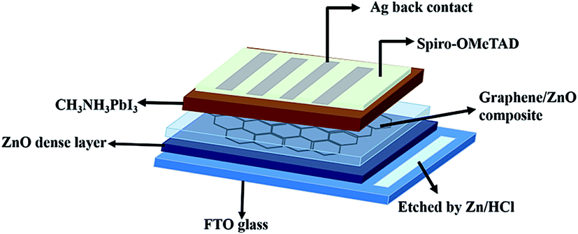 | ||
| Fig. 1 Schematic of the perovskite solar cell architecture fabricated using G/ZnO nanocomposite as an electron transporting layer. | ||
2.2. Characterization
The structure and surface morphology of perovskite films were analyzed by X-ray diffractometer (XRD, Rigaku Ultima-IV, Japan), scanning electron microscope (SEM, Carl-ZEISS EVO-18 microscope), respectively. The surface roughness of perovskite films was estimated by atomic force microscope (AFM, Bruker, Dimension Icon). Optical measurements were conducted by Perkin-Elmer lambda (1050) spectrophotometer. Photoluminescence (PL) spectra of perovskite films were recorded by Edinburgh instrument with an excitation wavelength of 530 nm. Current density–voltage (J–V) characteristics of PSCs were recorded by an Agilent 4155C semiconductor parameter analyzer, and with an illumination light intensity of ∼100 mW cm−2 (Xenon arc lamp with an air mass 1.5 filter from Newport). An NREL calibrated photodetector was used for intensity calibration by adjusting the distance between Xenon arc lamp and solar cell. Incident photon to current conversion efficiency (IPCE) measurements were carried out by a Xenon lamp (Newport) attached to a monochromator (Newport). Two lenses were used to focus a monochromatic light on an active area of a PSC. An NREL calibrated photodiode also was used as a reference for calibrating the IPCE system before the measurements.3. Results and discussion
In Fig. 2, we presented the XRD patterns of the ZnO film (on a bare glass substrate) and perovskite film (on ZnO/FTO-coated glass substrate). The Fig. 2a shows four diffraction peaks at 2θ = 31.75°, 34.32°, 36.27° and 47.52°, which correspond to the (100), (002), (101), and (102) planes of the wurtzite ZnO structure, and these peaks are in good agreement with the JCPDS data card no. 36-1451.18 The Fig. 2b shows the diffraction pattern of perovskite film, the diffraction peaks are from [(110), (200), (202), (211), (004), (310), and (314)] planes of tetragonal phase of the perovskite structure, which are in good agreement with reported literature.19 The other diffraction peaks in the Fig. 2b at 2θ = 26.42°, 37.68°, and 40.48° related to the FTO glass substrate (indicated by an asterisk) along with some ZnO diffraction peaks. Fig. 2c shows the diffraction pattern of graphene having a sharp diffraction peak ∼26.5°. In the case of the G/ZnO NC (Fig. 2d), there is no diffraction peak related to the graphene, which is due to the presence of tiny quantities of graphene. Hence, the XRD pattern of the G/ZnO NC is nearly same as that of ZnO (Fig. 2a). The XRD patterns of perovskite sensitized ZnO and G/ZnO NC have shown in the Fig. 2d. We have observed an intense diffraction peak of (110) at ∼14.1° related to the perovskite material from the G/ZnO NC film, in comparison to the pristine ZnO film. Which indicate the graphene role in the better growth of perovskite thin film with an improvement in the crystallinity.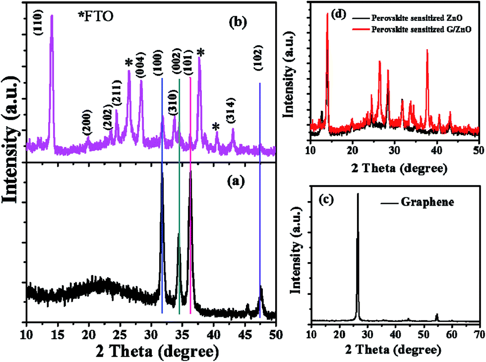 | ||
| Fig. 2 XRD patterns of (a) spray deposited ZnO film on a glass substrate, (b) perovskite film on a ZnO/FTO-coated glass substrate, (c) graphene and (d) perovskite sensitized ZnO and G/ZnO nanocomposite films. | ||
Apart from a crystal structure, the surface morphology of perovskite film also plays a crucial role in the photovoltaic performance. The simple spray deposition method can affect the ZnO and G/ZnO NC films growth, and later the perovskite films morphology during the growth. The SEM images of pristine ZnO and 0.75 wt% G/ZnO NC films have shown in Fig. 3. The difference between surface morphologies of pristine ZnO and G/ZnO NC films is not much, except a very small variation in the grain growth. The SEM and AFM micrographs of the perovskite films on pristine ZnO and 0.75 wt% G/ZnO NC films are presented in Fig. 4. One can see the large difference in the perovskite films grain growth from the nearly similar morphologies of the pristine ZnO and G/ZnO NC films. The perovskite film on the pure ZnO film resulted in non-uniformity with small grain sizes (10 to 100 nm), and the grains are close to each other with some pin holes (Fig. 4a). Whereas in the case of the perovskite film on the G/ZnO NC film resulted in improvement of the grain size of 200–250 nm (Fig. 4c). The perovskite film on the ZnO film has shown a large root mean square (RMS) roughness of ∼114 nm (Fig. 4b), whereas on the G/ZnO NC has shown the RMS roughness of ∼61 nm only (Fig. 4d). The graphene in the NC has facilitated the infiltration of perovskite precursor (with better loading), and then the formation of the smooth film with an improvement in surface morphology of the perovskite layer. The large grain size perovskite layer helps with the better carrier mobility by reducing the defect and trap states from the perovskite grain boundaries.20 In addition, we have carried out the TEM analysis to confirm the uniform distribution of graphene in the nanocomposite. The TEM images of graphene and G/ZnO NC have shown in Fig. 5a and b, respectively. From Fig. 5b, one can see the presence of graphene sheets among the ZnO nanoparticles. We also recorded the Raman spectrum of graphene (inset of Fig. 5a), it consists of ‘D’ (defect) and ‘G’ (graphitic) bands around 1349 cm−1 and 1590 cm−1, respectively.
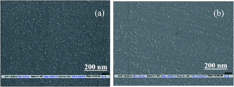 | ||
| Fig. 3 SEM images of (a) ZnO and (b) 0.75 wt%. G/ZnO nanocomposite films. | ||
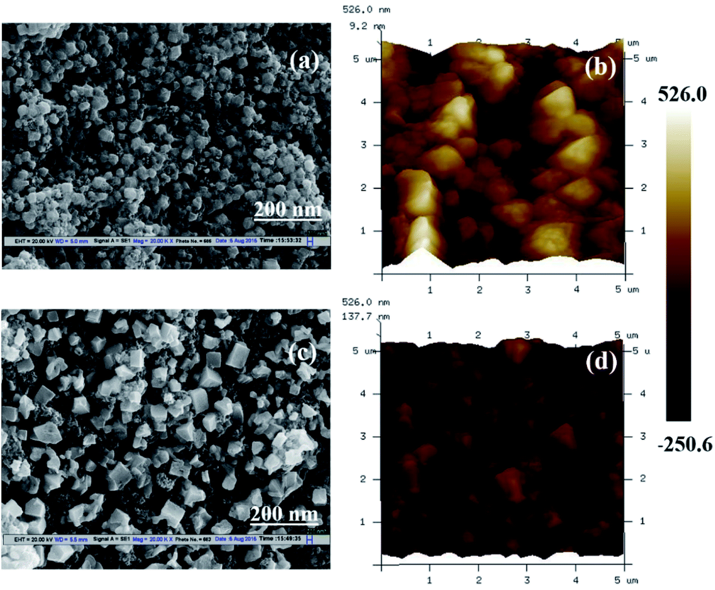 | ||
| Fig. 4 SEM and AFM micrographs of perovskite films prepared on ZnO film (a and b), and on 0.75 wt% G/ZnO nanocomposite film (c and d) coated on glass substrates, respectively. | ||
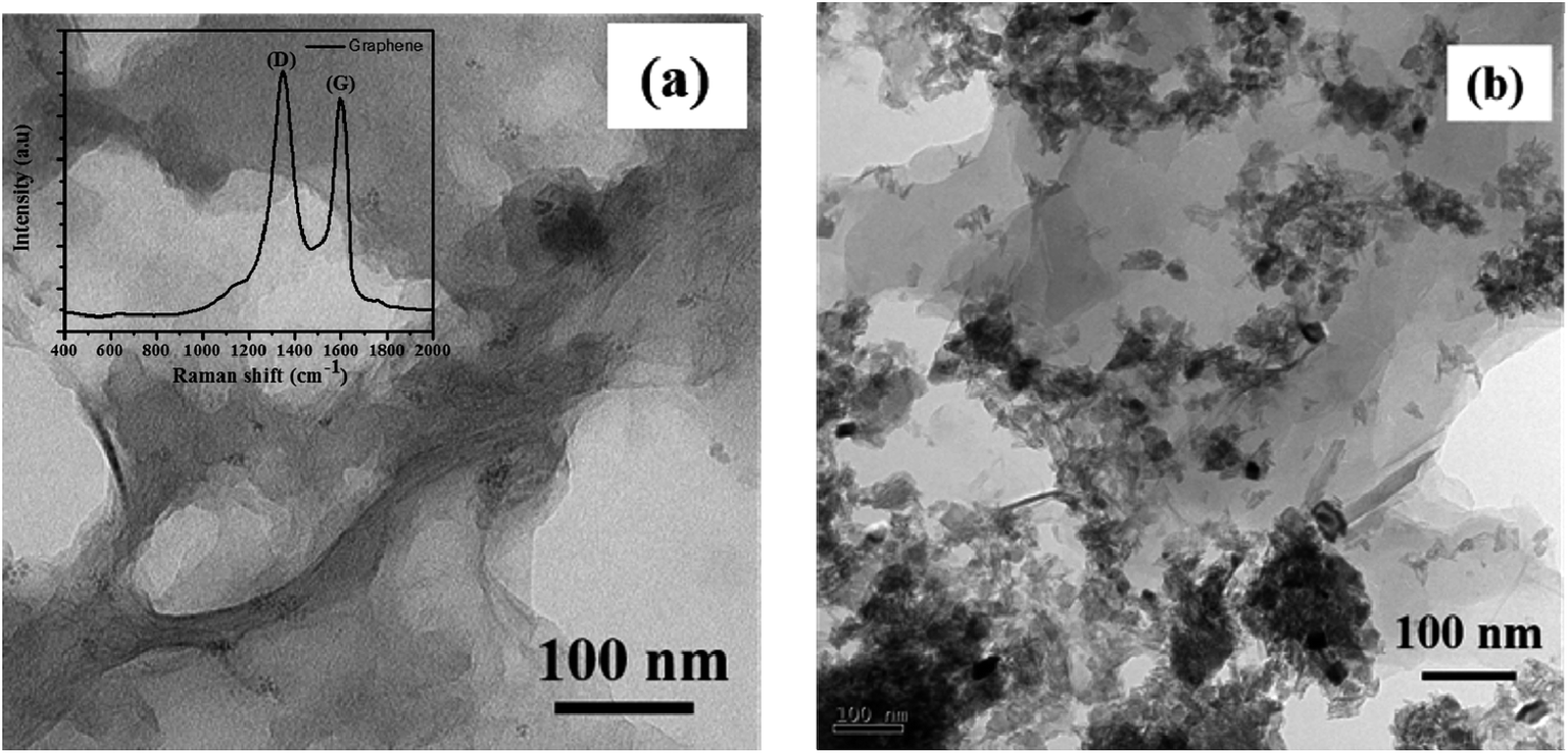 | ||
| Fig. 5 TEM images of (a) graphene, (b) G/ZnO nanocomposite and inset of (a) shows the Raman spectrum of graphene. | ||
The absorption spectra of perovskite films (on the ZnO and G/ZnO NCs) are presented in Fig. 6a. The films have exhibited a broad range of light absorption (from 350 to 760 nm), with an increase of graphene concentration in the NC films the absorption in perovskite films also increased linearly. In our case, the bare perovskite film has shown the lower absorbance than the normal absorbance of perovskite film (thickness of 350–400 nm) reported in the literature,21–23 due to the smaller thickness of ∼200 nm. The large surface area of graphene sheets in the nanocomposite enhanced the perovskite anchoring around the graphene, which facilitated an improvement in the grain growth and further the absorption. The PL measurements are also carried out to understand the charge carrier recombination in the perovskite films without and with different concentration of the graphene in the ZnO film. The perovskite film on the bare ZnO has shown a broad emission peak at ∼780 nm (Fig. 6b); whereas with the G/ZnO NC, the PL is quenched significantly and it is slightly sensitive to the graphene concentration. The PL intensity reduction of perovskite films with the graphene is due to efficient charge carrier extraction by the graphene network in the NC film.24
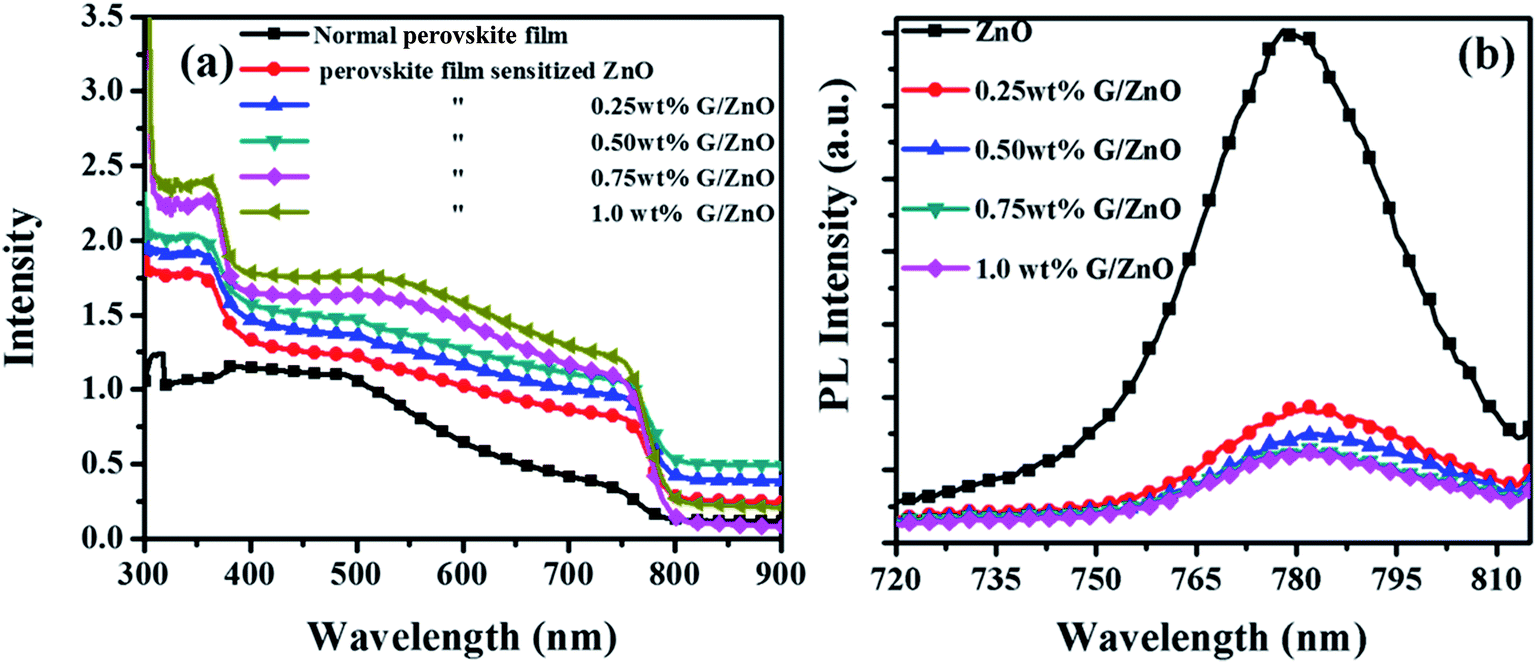 | ||
| Fig. 6 (a) Absorbance and (b) photoluminescence spectra of perovskite films on G/ZnO nanocomposites with different graphene concentration. | ||
For PSC performance evaluation based on the G/ZnO NC as an ETL, the J–V and IPCE measurements are conducted and their corresponding graphs are presented in Fig. 7a and b, respectively, the photovoltaic parameters are summarized in Table 1. With an increase in the concentration of graphene in the NC; the short-circuit current density (Jsc), open circuit voltage (Voc), fill factor (FF) and PCE are enhanced up to a certain concentration, then after the cell performance is deteriorated. With 0.75 wt% graphene concentration in the NC, the device has exhibited an improvement in Jsc from 15.54 mA cm−2 to 19.97 mA cm−2, and the PCE from 7.01% to 10.34%. The IPCE measurements have also supported an enhancement in the photocurrent from the PSCs (Fig. 7b). One can observe the graphene concentration dependent enhancement in the IPCE, more than 75% of photon-to-current conversion efficiency is observed with the graphene, whereas without the graphene the IPCE is limited to ∼55%.
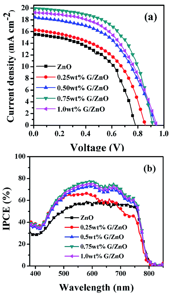 | ||
| Fig. 7 (a) Current density–voltage graphs and (b) incident photon to current conversion efficiency (IPCE) spectra of perovskite solar cells prepared by the G/ZnO composites with different graphene concentration. | ||
| Device | Voc (V) | Jsc (mA cm−2) | FF (%) | PCE (%) |
|---|---|---|---|---|
| 0.0 wt% G/ZnO | 0.792 ± 0.03 | 15.54 ± 0.98 | 51.64 ± 1.24 | 7.01 ± 0.66 |
| 0.25 wt% G/ZnO | 0.861 ± 0.02 | 16.34 ± 0.95 | 52.41 ± 1.08 | 7.36 ± 0.08 |
| 0.50 wt% G/ZnO | 0.943 ± 0.05 | 18.44 ± 1.31 | 50.81 ± 1.56 | 8.81 ± 0.17 |
| 0.75 wt% G/ZnO | 0.926 ± 0.07 | 19.97 ± 1.08 | 56.31 ± 1.18 | 10.34 ± 0.18 |
| 1.00 wt% G/ZnO | 0.951 ± 0.04 | 19.24 ± 0.76 | 51.23 ± 1.36 | 9.37 ± 0.48 |
The G/ZnO NC has facilitated for uniform bigger grains and small surface roughness perovskite films growth (Fig. 4c and d). In the PSCs, an ETL plays a crucial role, which can hinder electron transport due to grain boundary scattering and with the recombination process. With the graphene in the NC, an electron transport is accelerated due to better charge extraction and conductivity. The intimate contact between the G/ZnO and perovskite film also can lead to a reduction in interfacial resistance and further an improvement in charge collection efficiency. There is also an optimum energy band alignment between the G/ZnO NC and perovskite,25 due to this the electrons can easily transfer from the perovskite material to the NC.15 Relatively large size perovskite crystals on the G/ZnO NCs can also scatter the incoming light efficiently, increasing the photon recycling efficiency as studied recently by Friend et al.26,27 Large crystals can redirect the light from off-normal and thereby improve the effective optical path length of a device.19 So, the efficient charge extraction and improved mobility under the presence of graphene network in the NC and to some extent the light forward scattering with the NC are responsible for an enhancement in the Jsc and PCE of the PSC. However, with a large concentration of graphene (1.0 wt%), the device performance is affected adversely despite an improvement in light absorption (Fig. 6a). It could be due to a parasitic absorption by the graphene itself,16 and also a direct contact between the graphene and perovskite can lead to an inferior charge selective electrode with charge carrier recombination.15 Below 0.75 wt% of graphene concentration in the NC; the perovskite precursor loading may not be sufficient to grow uniform films with appropriate morphology, due to this there is no considerable improvement in the photovoltaic performance of the device. However, there was a gradual improvement in the photovoltaic performance with an increase in the graphene concentration. So, there should be an optimum graphene concentration (0.75 wt% graphene, as per our findings) in the NC for better infiltration of perovskite precursor into a scaffolding layer, and also for providing an efficient charge transport mechanism after photo-carrier generation in a device structure.
4. Conclusions
In summary, we have demonstrated the role of graphene concentration in the PSC performance after incorporating in the G/ZnO NC electron extraction layer. With the graphene, we have observed an improvement in perovskite film grains growth and further short circuit currents and power conversion efficiencies. The interfacial modification of the ZnO with graphene is led to significant power conversion efficiency due to an enhancement in the charge transport/extraction, optimum 0.75 wt% of graphene in the NC resulted in the best PSC performance. This work can open the new avenues for achieving the higher efficiencies of solar cells with the better electron transport layers from the NCs.Acknowledgements
P. S. Chandrasekhar sincerely thank Department of Science and Technology (DST), Govt. of India for granting fellowship under DST INSPIRE Fellowships (Code No. IF-120755) program. The authors would like to thank Nanoscale and Central Research Facilities (NRF & CRF) of IIT Delhi for their kind help in characterization.References
- B. V. Lotsch, Angew. Chem., Int. Ed., 2014, 53, 635–637 CrossRef CAS PubMed.
- A. Kojima, K. Teshima, Y. Shirai and T. Miyasaka, J. Am. Chem. Soc., 2009, 131, 6050–6051 CrossRef CAS PubMed.
- N. J. Jeon, J. H. Noh, W. S. Yang, Y. C. Kim, S. Ryu, J. Seo and S. I. Seok, Nature, 2015, 517, 476–480 CrossRef CAS PubMed.
- NREL Chart, http://www.nrel.gov/ncpv/images/efficiency_chart.jpg, accessed, 13.03.2016.
- H. S. Kim, I. Mora-Sero, V. Gonzalez-Pedro, F. Fabregat-Santiago, E. J. Juarez-Perez, N. G. Park and J. Bisquert, Nat. Commun., 2013, 4, 2242 Search PubMed.
- H. S. Kim, C. R. Lee, J. H. Im, K. B. Lee, T. Moehl, A. Marchioro, S. J. Moon, R. Humphry-Baker, J. H. Yum, J. E. Moser, M. Gratzel and N. G. Park, Sci. Rep., 2102, 2, 591, DOI:10.1038/srep00591.
- J. H. Noh, S. H. Im, J. H. Heo, T. N. Mandal and S. I. Seok, Nano Lett., 2013, 13, 1764–1769 CrossRef CAS PubMed.
- M. Zhang, M. Lyu, H. Yu, J. H. Yun, Q. Wang and L. Wang, Chem.–Eur. J., 2015, 21, 434–439 CrossRef CAS PubMed.
- Z. Zhu, X. Zheng, Y. Bai, T. Zhang, Z. Wang, S. Xiao and S. Yang, Phys. Chem. Chem. Phys., 2015, 17, 18265–18268 RSC.
- J. Qiu, Y. Qiu, K. Yan, M. Zhong, C. Mu, H. Yan and S. Yang, Nanoscale, 2013, 5, 3245–3248 RSC.
- D. Liu and T. L. Kelly, Nat. Photonics, 2014, 8, 133–138 CrossRef CAS.
- K. D. Kim, D. C. Lim, J. Hu, J. D. Kwon, M. G. Jeong, H. O. Seo, J. Y. Lee, K. Y. Jang, J. H. Lim, K. H. Kee, Y. Jeong, Y. D. Kim and S. Cho, ACS Appl. Mater. Interfaces, 2013, 5, 8718–8723 CAS.
- M. Acik and S. B. Darling, J. Mater. Chem. A, 2016, 4, 6185–6235 CAS.
- G. S. Han, Y. H. Song, Y. U. Jin, J. W. Lee, N. G. Park, B. K. Kang, J. K. Lee, I. S. Cho, D. H. Yoon and H. S. Jung, ACS Appl. Mater. Interfaces, 2015, 7, 23521–23526 CAS.
- M. M. Tavakoli, R. Tavakoli, Z. Nourbakhsh, A. Waleed, U. S. Virk and Z. Fan, Adv. Mater. Interfaces, 2016, 3, 1500790 CrossRef.
- J. T. W. Wang, J. M. Ball, E. M. Barea, A. Abate, J. A. AlexanderWebber, J. Huang, M. Saliba, I. Mora-Sero, J. Bisquert, H. J. Snaith and R. J. Nicholas, Nano Lett., 2014, 14, 724–730 CrossRef CAS PubMed.
- Y. Cheng, Q. D. Yang, J. Xiao, Q. Xue, H. W. Li, Z. Guan, H. L. Yip and S. W. Tsang, ACS Appl. Mater. Interfaces, 2015, 7, 19986–19993 Search PubMed.
- K. Mahmood, S. B. Park and H. J. Sung, J. Mater. Chem. C, 2013, 1, 3138–31349 RSC.
- D. Liu, M. K. Gangishetty and T. L. Kelly, J. Mater. Chem. A, 2014, 2, 19873–19881 CAS.
- D. Liu and T. L. Kelly, Nat. Photonics, 2014, 8, 133–138 CrossRef CAS.
- Z. L. Tseng, C. H. Chiang and C. G. Wu, Sci. Rep., 2015, 5, 13211, DOI:10.1038/srep13211.
- D. Zhao, Y. Yu, C. Wang, W. Liao, N. Shrestha, C. R. Grice, A. J. Cimaroli, L. Guan, R. J. Ellingson, K. Zhu, X. Zhao, R. G. Xiong and Y. Yan, Nat. Energy, 2017, 2, 17018 CrossRef CAS.
- K. Wang, C. Liu, P. Du, L. Chen, J. Zhu, A. Karim and X. Gong, Org. Electron., 2015, 21, 19–26 CrossRef CAS.
- K. Yan, Z. Wei, J. Li, H. Chen, Y. Yi, X. Zheng, X. Long, Z. Wang, J. Wang, J. Xu and S. Yang, Small, 2015, 11, 2269–2274 CrossRef CAS PubMed.
- X. Xiu, H. Zhang, J. Shi, J. Dong, Y. Luo, D. Li and Q. Meng, J. Mater. Chem. A, 2015, 3, 19288–19293 Search PubMed.
- L. M. P. Outon, M. Szumilo, R. Lamboll, J. M. Richter, M. C. Quesada and A. Mojtaba, Science, 2016, 351, 1430–1433 CrossRef PubMed.
- J. M. Richter, M. A. Jalebi, A. Sadhanala, M. Tabachnyk, J. P. H. Rivett, L. M. Pazos-Outon, K. C. Godel, M. Price, F. Deschler and R. H. Friend, Nat. Commun., 2016, 7, 13941 CrossRef CAS PubMed.
| This journal is © The Royal Society of Chemistry 2017 |