 Open Access Article
Nanowire Y-junction formation during self-faceting on high-index GaAs substrates
R. Méndez-Camachoa,
M. López-Lópezb,
V. H. Méndez-Garcíaa,
D. Valdez-Pérezc,
E. Ortegad,
A. Benitezd,
A. Ponce d and
E. Cruz-Hernández
 *a
*a
aCoordinación para la Innovación y la Aplicación de la Ciencia y la Tecnología (CIACYT), Universidad Autónoma de San Luis Potosí, Sierra Leona 550, S. L. P. 78210, México. E-mail: esteban.cruz@uaslp.mx
bPhysics Department, CINVESTAV-IPN, Apartado Postal 14-740, México D.F. 07000, México
cInstituto Politécnico Nacional, UPALM, Edif. Z-4 3er Piso, 07738, México D.F., México
dDepartment of Physics and Astronomy, The University of Texas at San Antonio, One UTSA Circle, San Antonio, TX 78249, USA
First published on 23rd March 2017
Abstract
A major current focus in nanotechnology is the precise control of the self-assembling of semiconductor structures at the nanometric level. Highly uniform structures such as quantum wires can now be fabricated from the self-assembly of nanometric facet arrays produced using high-index substrates and epitaxial techniques. However, the self-assembling of more complex nanostructures such as Y-junctions is a more involved problem, hindering potential technological applications and one-dimensional physics exploration. In this contribution, we report on the observation of high-order and two-dimensional mechanisms in the Molecular Beam Epitaxy growth of GaAs on (6 3 1) oriented GaAs substrates. These mechanisms allow the formation of a regular alternating pattern of bifurcated nanowires, the Y-junctions. The Y-junction/nanowire arrays have suitable dimensions to form a one-dimensional electron gas device by use of a modulation doping structure with a source, a drain, and gate electrodes. Finally, the potential use of the bifurcated structures for the exploration of one-dimensional transport and as a viable alternative to carbon nanotube Y-junctions is discussed.
1 Introduction
Among the number of growth techniques available to achieve the challenging task of precisely controlling the self-assembling of semiconductor nanostructures such as quantum dots or quantum wires (QWRs), Molecular Beam Epitaxy (MBE) is especially able to produce the ordered formation of crystalline nanostructures. This control can be achieved using tactics, such as the structural stress from dissimilar materials to form quantum dots,1,2 or by growing on high-index substrates to grow uniform one-dimensional facet (1DF) arrays, which are useful as nano-templates to form QWRs.3–5 In MBE the growth process is carried out under non-equilibrium conditions, then nonlinear evolution processes, such as step-bunching,6 meandering instabilities,7 and coarsening,8 produce a very rich variety of surface morphologies, which in turn must be understood to precisely control the self-assembly of complex nanostructures.In previous work, in the homoepitaxy of 1 μm thick layers on GaAs(631)A substrates grown by MBE, at a slow growth rate of 0.3 μm h−1, a high Tg of 700 °C, an optimal As/Ga ratio, and a long deposition time, a quasi-stationary state was established to induce the formation of almost perfect 1DF nanometric arrays in areas of up to 1 × 1 μm2. Furthermore, a high uniformity in 5 × 5 μm2 areas presenting 1DF coherent lengths up to 3.6 μm was also achieved,9 ensuring a one-dimensional (1D) electronic transport length larger than the electronic quantum coherence.10 Similar results have been reported by other groups by using substrates oriented in different high-index directions.3,4 However, for areas larger than 1 μm2 a loss of uniformity is frequently observed, indicating that unknown long-range mechanisms play an important role in the 1DF growth process.
In this work, using long-range mechanisms that are present in the 1DF MBE synthesis on high-index substrates, a method to self-assemble an alternating array of Y-junctions and nanowires is presented.
2 Experimental
In order to induce the formation of uniform nanometric arrays of 1DFs, homoepitaxial layers on GaAs (631)A semi-insulating substrates were grown by MBE, following similar experimental conditions published elsewhere.9 Prior to the layers’ growth, the GaAs wafers were degreased, etched, and then loaded in a Riber 32 MBE system. Once transferred to the growth chamber, the oxide desorption process was carried out at 580 °C for 15 min under As4 overpressure. Next, a smoothing 100 nm thick GaAs layer was deposited at Ga and As beam equivalent pressures (BEPs) of 4 × 10⁻⁷ Torr and 5.5 × 10⁻⁶ Torr, respectively, at a growth temperature (Tg) of 600 °C. Finally, Tg was increased to 700 °C and, in order to explore different stages in the 1DF formation process, two different kinds of samples were grown at a growth rate of 0.6 μm h−1 with GaAs layers 500 nm (M1) and 1 μm (M2) thick.The samples’ surfaces were monitored in situ by reflection high-energy electron diffraction (RHEED). Atomic Force Microscopy (AFM) images were taken ex situ shortly after the MBE growth process, using a NanoScope IIIa multimode instrument (Digital Instruments, Santa Barbara, CA). A piezo-electric stage (E-scanner) with a maximum effective scan area of 15 × 15 μm2 was used. Tapping-mode silicon cantilever tips 125 μm in length, with a nominal 275–325 kHz resonance frequency and a 31.18–44.54 N m−1 spring constant were operated at room temperature in air. Images were typically obtained with scan rates of 0.5–1 Hz and collected in height mode, maintaining a constant force. Using this configuration, AFM images clearly resolving the 1DF morphology were obtained. In order to identify crystallographic planes in the modulated 1D structure we have performed aberration-corrected scanning transmission electron microscopy (STEM) using a high angle annular dark field detector (HAADF). The sample was prepared using a focused ion beam system (Zeiss model CrossBeam 340) coupled with a manipulator to extract the sample to be studied in cross section view. HAADF-STEM images were collected oriented in the zone axis 〈112〉.
3 Results and discussion
During faceting by MBE, the evolution of the 1DF can roughly be divided into three different stages.6,8,11 (i) An initial stage where dynamical processes play the main role in inducing, by step-bunching, a 1DF-like array of short period terraces (<10a0, where a0 is the GaAs lattice constant) from the original bulk-truncated atomic array. (ii) In the second stage, when the period of the terraces is larger than 10a0, the elastic and coarsening effects become important but they do not establish a stationary stage so a non-optimal and non-unique lateral period can be reached in the 1DF. (iii) When the system reaches a stationary state, the lateral period of the facets slowly increases up to a quasi-constant, optimal value predicted from both the elastic and coarsening theories. In this work, we report results from samples grown under two different conditions: in stage (ii), sample M1 (0.5 μm-thick), and in stage (iii), sample M2 (1 μm-thick).3.1 Early stages
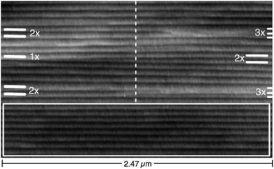
In contrast to the stationary stage (iii), where the final surface morphology is quite uniform across all of the sample, at stages (i) and (ii) the samples present a variety of morphologies across their surfaces triggered by the interplay between coarsening, elastic, and dynamical processes (see Fig. 1, 2 and 3a and b).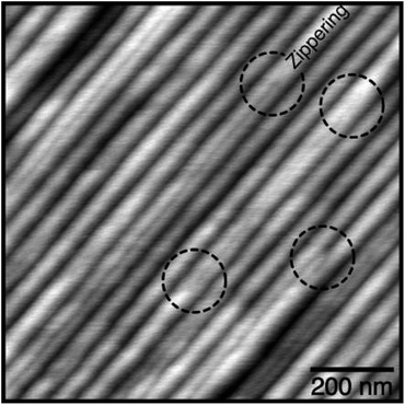 | ||
| Fig. 2 A 1 × 1 μm2 AFM image of sample M1 showing a zipper-like mechanism along the longitudinal direction of the 1DF. | ||
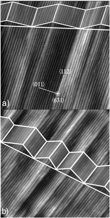 | ||
| Fig. 3 3 × 3 μm2 AFM images of sample M1 showing high-order modulation, which is schematically drawn on the sample. | ||
In Fig. 1 we show an AFM image of sample M1. Two typical surface morphologies can be observed from this image: almost perfect 1DF arrays (running parallel over distances of up to 2.5 μm, in the region marked by a rectangle) and bifurcated 1DF structures, which are composed of a single 1DF (1×) connected with a double 1DF (2×) or even with a triple 1DF (3×), all oriented along the same direction. Also from Fig. 1 we can observe that the distribution of these structures vaguely follows an alternating pattern in both the longitudinal and the transverse directions of the 1DF. Furthermore, it is in an established well-defined region (vertical dotted line) where the transition from 1×–2×, 2×–1× or 2×–3× occurs. Similar surface morphologies are observed at stage (iii), with some important differences, as we will discuss later.
Fig. 2 shows the existence of a zipper-like mechanism in the 1DF formation at stage (ii). This zipper-like mechanism is similar to the step-bunching process; adatoms diffuse along the 1DF, find a step in the union of the 1× side with the 2× side of the bifurcated structures (the Y-junctions), sticking at the edges, then produce the 1× side of the Y-junctions by zippering the 2× side.
3.2 High-order modulation
To deepen the investigation into the Y-structures’ formation mechanism, we carried out an auto correlation function (ACF) analysis from the AFM images. In Fig. 3a and b we show two 3 × 3 μm2 AFM images taken in different regions of sample M1. The uniform regions show the formation of almost perfect 1DFs running up to distances of 3 μm, with an average lateral period (Dp) between 65 and 70 nm and a height between 1.5 and 2 nm.In Fig. 4a we show the ACF image obtained from the 3 × 3 μm2 AFM image in Fig. 3a, showing that for this relatively large area the coherency of the facet morphology is almost lost. In contrast, by taking the ACF in a 1 × 1 μm2 uniform region of M1, a highly coherent pattern can be observed (Fig. 4b). Dp has been quantitatively evaluated by fitting the ACF profiles with a damping sinusoidal function of the form
 | (1) |
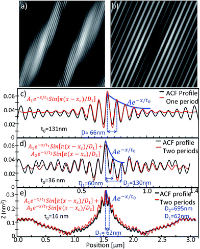 | ||
| Fig. 4 (a) An ACF image obtained from the 3 × 3 μm AFM image in Fig. 3a and (b) an ACF image obtained from a uniform 1 × 1 μm2 area taken from Fig. 3a. ACF profiles are shown with black lines for: (c) the uniform region shown in (b), (d) a non-uniform 1 × 1 μm2 region in Fig. 3a, and (e) the 3 × 3 μm2 area shown in Fig. 3a. The red lines show the fitted damping sinusoidal function (eqn (1)). The corresponding values for the amplitude are: (c) A1 = 0.08 nm2, (d) A1 = 0.025 nm2, A2 = 0.065 nm2, and (e) A1 = 1.2 nm2, A2 = 0.12 nm2. | ||
Typically, for 1 × 1 μm2 uniform regions, damping constants of t0 ∼130 nm and Dp ∼65 nm are obtained (Fig. 4c). However, when applying the ACF to a non-uniform 1 × 1 μm2 area, the cross sectional ACF profile must be fitted by two single sinusoidal functions with different periods, D1 ∼60 nm and D2 ∼130 nm (Fig. 4d). The D1 oscillation can be related to the single 1DF while the D2 oscillation can be related to the junction of two of these single 1DF structures. The low value of the damping constant (t0 ∼ 36 nm) reflects the loss of coherence of the single 1DF array in this region.
However, when a larger AFM area is analyzed (Fig. 3a), the ACF shows quite different behavior (Fig. 4a). For a relatively large 3 × 3 μm2 area, the cross sectional profile (Fig. 4e) must be fitted by a double damping sinusoidal function, with periods of D1 ∼62 nm and D2 ∼695 nm and a damping constant of t0 ∼16 nm. As before, D1 can be assigned to the single 1DF. However, the unexpectedly large D2 value reveals the existence of an underlying high-order surface modulation that coexists with the nanometric 1DFs (as schematically shown in Fig. 3a and b and 5).
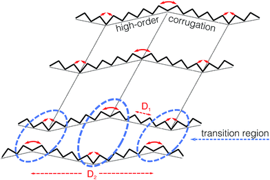 | ||
| Fig. 5 Schematic representation of the underlying modulation and the formation mechanism behind the alternating array of Y-junctions. | ||
The subjacent large-order corrugation has a direct connection with the formation of the Y-junctions. As observed in Fig. 3a and b, the Y-junctions appear at the edge of the high-order modulation, while at the lateral sides of this high-order modulation uniform arrays of 1DF are promoted. To our knowledge, the existence of such underlying high-order surface modulation has not been reported before. Furthermore, even when this modulation must be produced by some long-range elastic interactions, clearly it does not follow the behavior described by the usual Marchenko formalism11 of elastic faceting.
3.3 Crystallographic planes
Using STEM, we have analyzed the crystalline characteristics of the 1DFs. Fig. 6a shows a high resolution microscope HAADF-STEM image indicating the perfect crystallinity of the facets and the angles measured at the atomic level. The faceted plane identified with respect to the {111} plane is the {11 5 2} plane. In Fig. 6b a fast Fourier transform (FFT) image indicates the directions and the zone axis. Fig. 6c shows a lower resolution HAADF-STEM image in which the projection of two 1DFs is included. From Fig. 6a we can establish the values of 2.5 nm and 17 nm for the height and Dp of the 1DF, respectively. To clarify the apparent incompatibility between the values of Dp observed from HAADF-STEM and AFM, we must consider that the prepared lamella used to observe the facets by STEM is around 10–12 μm thick so the STEM image is composed of the projection of non-collinear 60 nm facets. The observed Dp values of 17 nm correspond to the projection of 3 of these non-collinear facets, which is consistent with the Y-junction dimensions observed by AFM.3.4 Formation of nanowire Y-junctions
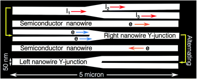
In Fig. 7 we show a 4.7 × 2.4 μm2 AFM image of sample growth at stage (iii), of sample M2. Almost perfect 1DF arrays (running parallel over distances up to 5 μm, region marked by a rectangle) and bifurcated 1DF structures or Y-junctions can be observed. In Fig. 7 the distribution of the Y-junction structures follows an alternating pattern in both the longitudinal and the transverse directions, as schematized in Fig. 8.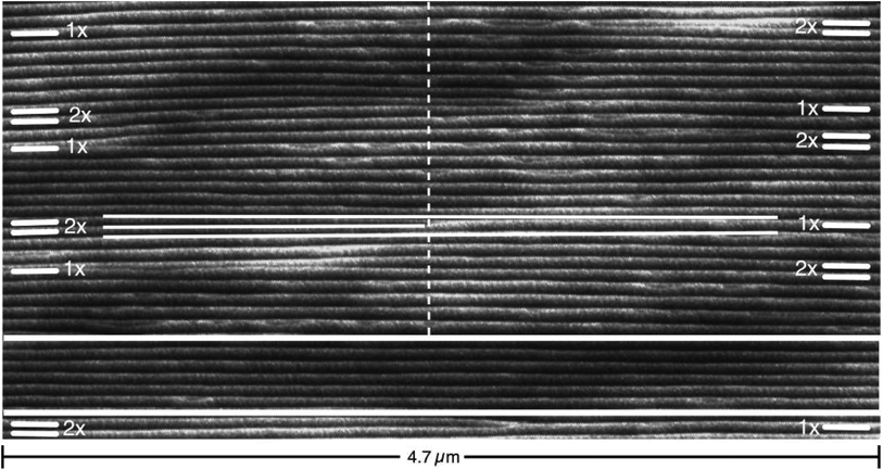 | ||
| Fig. 7 An AFM image of sample M2. The uniform region is shown inside the rectangle. The alternating pattern of the Y-structures in both the longitudinal and transverse directions is highlighted. | ||
By counting the number of Y-structures and single 1DFs running side by side in a 5 μm × 5 μm area, we can make an estimate of the average maximal length of the 1DF before it turns into a double 1DF. In a 5 μm × 5 μm area there are on average six single 1DFs for each Y-structure. Extrapolating this result we can estimate that, if we assume that every 1DF in a region is bifurcated, each Y-structure would have an extension as large as 35 μm. That is, on average, for samples grown in stage (iii) there are single 1DFs running perfectly uniformly up to a distance of 17.5 μm. These are remarkable results for potential applications of QWRs,12–15 Y-junctions,16–18 or arrays of both of them (see Fig. 8).
3.5 Potential applications
It is worth noting that even when the loss of uniformity introduced by the formation of Y-junctions is considered as a drawback for QWR applications (where a perfectly uniform array could be preferred, such as if the 1DF array is used as template to grow semiconductor quantum heterostructures using, for example, GaAs/AlGaAs or InAs/GaAs systems5), the very elongated Y-structures can be used to explore 1D physical phenomena. For instance, the electronic transport along these structures could give valuable information about what happens when two independent 1D electronic gases moving along the 2× side are forced to join in a single 1D electronic channel. Inversely, it could be also possible to get some valuable information on the way that a 1D electronic gas splits into two 1D electronic gases. Such experiments could be used to inquire about fundamental 1D phenomena.19–22 The Y-junctions/nanowire arrays could be also important for nanoelectronics in applications such as ballistic switching and rectification, which have been only explored using carbon nanotube Y-junctions.16–18Finally, we would like to stress that the latter longitudinal mechanism is not described by the usual (only transverse) models of elastic and coarsening theories.8,11,23–25 Neither of these models describes the formation of the long-range pattern of the Y-structures in both the transverse and longitudinal directions, so an elastic formalism must be developed in order to model this bi-dimensional long-range modulation, which is out of the scope of this contribution.
4 Conclusions
In conclusion, we report the observation of high-order and bi-dimensional mechanisms in 1D MBE faceting on high-index substrates. We found that a long-range subjacent modulation has an important influence on the 1DF arrays. This modulation can be used to produce arrays of semiconductor nanoscale Y-junctions and nanowires, which in turn could have important applications in nanoelectronic devices or in 1D electronic transport fundamental investigation.Acknowledgements
Authors acknowledge partial financial support from CONACYT, grant 257434. The microscopy work was supported by the National Institute on Minority Health and Health Disparities (NIMHD) in the program Research Centers in Minority Institutions Program (RCMI) Nanotechnology and Human Health Core (G12MD007591).References
- J. M. Moison, F. Houzay, F. Barthe, L. Leprince, E. André and O. Vatel, Appl. Phys. Lett., 1994, 64, 196–198 CrossRef CAS.
- D. Leonard, M. Krishnamurthy, C. M. Reaves, S. P. Denbaars and P. M. Petroff, Appl. Phys. Lett., 1993, 63, 3203–3205 CrossRef CAS.
- M. Yamamoto, M. Higashiwaki, S. Shimomura, N. Sano and S. Hiyamizu, Jpn. J. Appl. Phys., 1997, 36, 6285–6289 CrossRef CAS.
- Z. Gong, Z. Niu and Z. Fang, Nanotechnology, 2006, 17, 1140–1145 CrossRef CAS PubMed.
- E. Cruz-Hernández, D. Vázquez-Cortés, A. Cisneros-de-la Rosa, E. López-Luna, V. H. Méndez-García and S. Shimomura, J. Vac. Sci. Technol., B: Microelectron. Nanometer Struct.–Process., Meas., Phenom., 2012, 30, 02B111 Search PubMed.
- W. K. Burton, N. Cabrera and F. C. Frank, Philos. Trans. R. Soc. London, Ser. A, 1951, 243, 299–358 CrossRef.
- G. S. Bales and A. Zangwill, Phys. Rev. B: Condens. Matter Mater. Phys., 1990, 41, 5500–5508 CrossRef.
- M. Guedda, H. Trojette, S. Peponas and M. Benlahsen, Phys. Rev. B: Condens. Matter Mater. Phys., 2010, 81, 195436–195443 CrossRef.
- E. Cruz-Hernández, S. Shimomura and V. H. Méndez-García, Appl. Phys. Lett., 2012, 101, 073112 CrossRef.
- M. Ferrier, L. Angers, A. C. H. Rowe, S. Guéron, H. Bouchiat, C. Texier, G. Montambaux and D. Mailly, Phys. Rev. Lett., 2004, 93, 246804 CrossRef CAS PubMed.
- V. I. Marchenko, Sov. Phys. JETP, 1981, 54, 605–607 Search PubMed.
- M. D. Kelzenberg, S. W. Boettcher, J. A. Petykiewicz, D. B. Turner-Evans, M. C. Putnam, E. L. Warren, J. M. Spurgeon, R. M. Briggs, N. S. Lewis and H. A. Atwater, Nat. Mater., 2010, 9, 239–244 CrossRef CAS PubMed.
- R. Yan, D. Gargas and P. Yang, Nat. Photonics, 2009, 3, 569–576 CrossRef CAS.
- M. H. Huang, S. Mao, H. Feick, H. Yan, Y. Wu, H. Kind, E. Weber, R. Russo and P. Yang, Science, 2001, 292, 1897–1899 CrossRef CAS PubMed.
- Y. Li, F. Qian, J. Xiang and C. M. Lieber, Mater. Today, 2006, 9, 1369–7012 Search PubMed.
- P. R. Bandaru, C. Daraio, S. Jin and A. M. Rao, Nat. Mater., 2005, 4, 663–666 CrossRef CAS PubMed.
- C. Papadopoulos, A. Rakitin, J. Li, A. S. Vedeneev and J. M. Xu, Phys. Rev. Lett., 2000, 85, 3476–3479 CrossRef CAS PubMed.
- A. N. Andriotis, M. Menon, D. Srivastava and L. Chernozatonskii, Appl. Phys. Lett., 2001, 79, 266–268 CrossRef CAS.
- S. Hofferberth, I. Lesanovsky, B. Fischer, T. Schumm and J. Schmiedmayer, Nature, 2007, 449, 324–327 CrossRef CAS PubMed.
- S. Kumar, K. Thomas, L. W. Smith, M. Pepper, G. L. Creeth, I. Farrer, D. Ritchie, G. Jones and J. Griffiths, Phys. Rev. B: Condens. Matter Mater. Phys., 2014, 90, 201304 CrossRef.
- M. Gring, M. Kuhnert, T. Langen, T. Kitagawa, B. Rauer, M. Schreitl, I. Mazets, D. A. Smith, E. Demler and J. Schmiedmayer, Science, 2012, 337, 1318–1322 CrossRef CAS PubMed.
- R. Méndez-Camacho, E. Cruz-Hernández and R. Castañeda Priego, Phys. Rev. B., 2017, 95, 085437 CrossRef.
- L. Feng, J. Tersoff and M. G. Lagally, Phys. Rev. Lett., 1998, 80, 1268–1271 CrossRef.
- V. Shchukin, N. Ledentsov, I. Soshnikov, N. Kryzhanovskaya, M. Maximov, N. Zakharov, P. Werner and D. Bimberg, Microelectron. J., 2006, 37, 1451–1460 CrossRef CAS.
- S. J. Watson, Proc. R. Soc. London, Ser. A, 2014, 471, 1–20 CrossRef.
| This journal is © The Royal Society of Chemistry 2017 |

