
 Open Access Article
 This Open Access Article is licensed under a
 Creative Commons Attribution 3.0 Unported Licence
A primary SERS-active interconnected Si-nanocore network for biomolecule detection with plasmonic nanosatellites as a secondary boosting mechanism†
Jeffery Alexander Powell a,
Krishnan Venkatakrishnan*ac and
Bo Tanb
a,
Krishnan Venkatakrishnan*ac and
Bo Tanb
aUltrashort Laser Nanomanufacturing Research Facility, Department of Mechanical and Industrial Engineering, Ryerson University, 350 Victoria Street, Toronto, M5B 2K3, ON, Canada. E-mail: venkat@ryerson.ca; Tel: +1-416-979-5000 ext. 4984
bNano-imaging Lab, Department of Aerospace Engineering, Ryerson University, 350 Victoria Street, Toronto, M5B 2K3, ON, Canada
cAffiliate Scientist, Keenan Research Center for Biomedical Science, St. Michael's Hospital, 30 Bond St, Toronto, M5B 1W8, ON, Canada
First published on 3rd July 2017
Abstract
We report in this study, the development of a polymorphic biosensitive Si nanocore superstructure as a SERS biosensing platform. The polymorphic Si nanostructure in this study is created through ultrafast pulse laser ion-plume (UPLIP) formation and we observe enhanced detection of L-glutathione (GSH). The distinctive polymorphic nanomaterial chemistry of the interconnected network of Si nanocores and the nanonetwork architecture of this nanostructure act as a primary enhancement booster (EF ∼ 6 × 10³). With the addition of Au/AuPd nanosatellites onto the surface of the polymorphic Si nanocore structure, a significant secondary boost in GSH enhancement is observed (EF ∼ 1 × 10⁵). The addition of noble metal nanostructures results in multi-source SERS enhancement that combines linked resonance enhancement and SPR mechanisms that both contribute to the detection and boosting of the biomolecule analyte signal. With this polymorphic Si primary booster and noble metal nanosatellite secondary booster, we have demonstrated the viability of Si nanostructures for SERS biosensing applications.
1. Introduction
Of the available techniques used for biosensing with nanomaterials, which include electrochemical,1 pyroelectric2 and optical techniques,3 SERS-based biomolecule detection offers distinctive advantages compared to the other methods including ultrahigh sensitivity4 and high specificity.5 For biomolecule detection with SERS, most sensing platforms utilize the surface plasmon resonance (SPR) mechanism characteristic of noble metal nanostructures (NMNs) as the primary source for SERS enhancement.6–8SERS active NMNs are used for the detection of biomolecule analytes such as glucose9 and nucleic acids.10 These SERS active NMNs are predominantly generated through the deposition of noble metal nanoparticles onto the surface of in-active nanostructures, which serves as a carrier platform for the SERS active noble metal nanoparticles.11,12 These quiescent scaffolding nanostructures are commonly semiconductor nanomaterials, such as Si nanowires,13 or Si nanostructures created by nanolithography14 or chemical synthesis.15,16 Currently, the detection of biomolecules with SERS is focused on mainly NMNs as a SERS activator while the underlying nanostructure has no reported SERS activity, to our knowledge.
However, there is a significant lack of research regarding the use of SERS biosensitive semiconductor nanostructures for bio-detection applications despite recent observations of semiconductor nanostructures having significant SERS activity.17,18 Furthermore, very little research has been conducted to establish Si as SERS biosensing platform due to the SERS in-active nature of traditionally fabricated Si nanostructures. The work by Lombardi and Birke19 define the fundamental principles of SERS activity of semiconductor nanomaterials. It has been recognized that several linked resonance mechanisms, each contribute to an observed semiconductor SERS enhancement;19 these mechanisms are plasmon resonance, exciton resonance and charge transfer resonance. These mechanisms work in tandem to increase an analyte signal, and a number of semiconductor materials have been shown to exhibit SERS enhancements with these linked resonances. Several nanomaterials, including TiO2,20 ZnS21 and CdSe22 have been shown to have significant sensing performance for chemical analytes. These nanostructures represent significant strides for semiconductor SERS chemical sensing, however these nanostructures are mostly limited to nanostructures such as nanoparticles18 or nanorods.23 Of the 3D SERS active nanostructures that include semiconductor nanostructures, nearly all of them rely these nanomaterials as a scaffolding or template for NMNs, which is reported as the sole SERS enhancement source.24 As such, the development of 3D semiconductor nanostructures as primary or co-contributors to the SERS enhancement of analyte detection is quite limited, especially for biomolecule sensing applications. We have previously studied the SERS enhancing characteristics of 3D silicon nanoweb structures for chemical sensing applications25,26 and have established these as active SERS nanostructures. While these semiconductors have received some research and development, to our knowledge the biosensing applications of semiconductor-based biosensing nanomaterials and specifically, self-assembled 3D Si nanostructures have yet to be explored.
In this study we introduce for the first time, to our knowledge, the concept of a Si nanocore enhancement mechanism for a boosted enhancement of biomolecule detection. In addition, we introduce the concept of a multi-source boosting mechanism for a further increase in enhancement of a biomolecule signal using a secondary SERS enhancement boost with the use of noble metal nanosatellites. The underlying principle is that, both a bio-SERS active Si semiconductor nanostructure platform and noble metal nanosatellites provide a primary and secondary boosting effect, respectively, on the biomolecule signal through independent enhancement mechanisms.
The SERS active Si nanocores act as a primary booster to the detection of a biomolecule analyte. The Si nanocore superstructure is comprised of a nanonetwork of fused Si nanospheroids that provide an enhancement of SERS biomolecule signal through linked resonance enhancement mechanism. The unique polymorphic structure of the Si nanocores and the self-assembled 3D nanonetwork morphology of the fused nanocores provides the SERS bio-activity not observed in traditionally fabricated Si nanostructures. The Au and AuPd nanosatellites act as a secondary boosting source for SERS biomolecule signal boosting by providing a SPR enhancement mechanism effect characteristic of NMNs. It is due to these primary, and secondary biomolecule signal boosting mechanisms working co-operatively, we observe that the biomolecule detection is significantly enhanced. In addition, by modifying the characteristics of the Si nanocore superstructure and the nanosatellites, we can achieve a balance between the two enhancement mechanisms that leads to greatly enhanced biomolecule detection.
By using the laser-ion plume formation mechanism to form the interconnected hybrid Si nanospheroid nanocore superstructure, we are forming a SERS biomolecule active 3D platform. For the deposition of Au nanosatellites or AuPd nanosatellites we use a physical ion deposition method; this combination of nanomaterials leads to a dual-contribution to SERS biomolecule enhancement from linked resonance enhancement and SPR, for a large increase in the enhancement of biomolecular sensing. To establish this Si nanostructure as a SERS biosensing nanomaterial, we have applied this material for the detection of L-glutathione (GSH), a tripeptide biomarker biomolecule present in living cells including cancer cells which indicates the amount of stress the cell is undergoing and as a result if a cell is dying.27,28 With the detection of this biomolecule, we aim to define the role of highly SERS biosensitive polymorphic Si nanostructure in the field of SERS biosensing. An overview of this study is presented in Fig. 1.
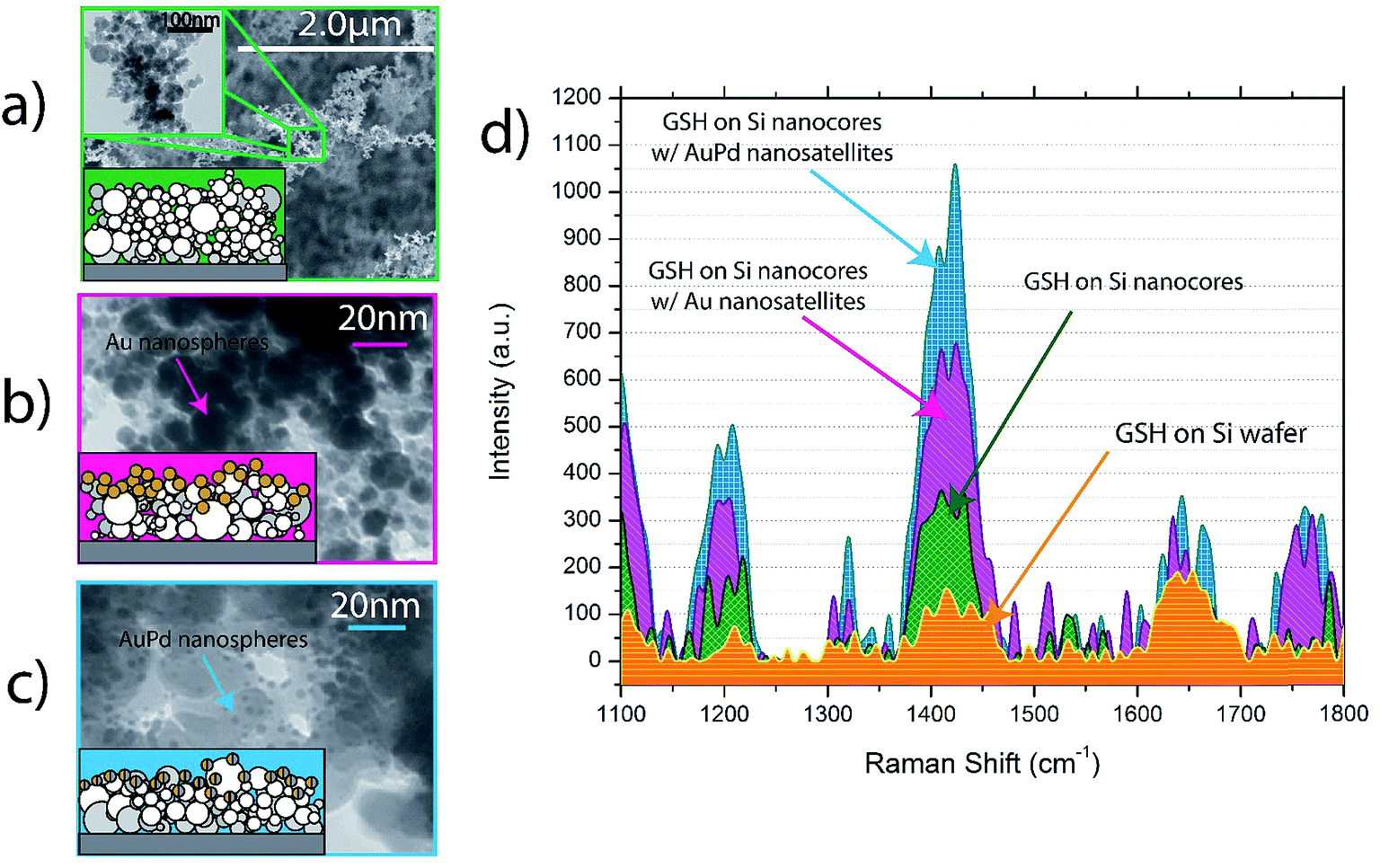 | ||
| Fig. 1 TEM and schematic diagrams of (a) Si nanocore structures (b) Si nanocores with Au nanosatellites (c) Si nanocores with AuPd nanosatellites and (d) Raman spectra showing GSH on each @532 nm wavelength. | ||
2. Experimental methods
The formation of the polymorphic Si nanocore structures are generated using a Clark-MXR IMPULSE pulsed Yb-doped fibre amplified femtosecond laser. With this pulsed laser system we are able to initiate the ultrafast pulsed laser ion plume (UPLIP) required to form a nanocore structure. In this study, 0.02 Ω cm p-type silicon (100) wafer substrates were used to create the polymorphic Si nanostructures. To have full control over UPLIP fabrication process, in this experiment the laser wavelength (1030 nm), polarization (circular), dwell time (0.5 ms), pulse width (214 fs) and the laser power (16 W) were kept static. The main UPLIP parameter varied in this study is the repetition rate of the laser, with which we can control the nanospheroid formation conditions of the laser ion plume. In order to create a consistent distribution of nanocore structures on the base Si wafer, the nanostructures were generated using a 300 × 300 point array with 25 micron point spacing; a piezo-driven raster was used to move the laser beam across the substrate surface using an array designed with EzCAD software.To coat the surface of the polymorphic Si nanocore structures with nanosatellites a physical deposition method was used; a 99.9% pure Au target and an AuPd target were bombarded with ion particles with an atmosphere of Argon gas to ionize the target. The ejected ions then physically deposit onto the surface of the nanocore structures for a set time. We have used the deposition time, 15 s established in our previous study, to increase maximize the SPR contribution from the nanosatellite structures.
For the acquisition of Raman spectra, a Bruker Optics SENTERRA Raman microscope was used using a 10× magnifying lens. Spectra of the Si nanocore nanostructures were obtained using 532 nm wavelength with a 10 s integration time and 3 iterations. To compare the polymorphic Si nanocores to the nanocores with Au or AuPd nanosatellites 5 mW power was used for 532 nm Raman spectra. For the GSH spectra acquisition, 10 μL of 10−6 M concentration GSH was applied to each nanocore substrate and Raman spectra were obtained using the same parameters above.
To determine the morphology of the nanocore structures and to measure and calculate the nanospheroid/nanosatellite sizes, high resolution tunnelling electron microscopy (HRTEM) images were obtained using a JEOL JEM-2010 HRTEM microscope. ImageJ software was used to manually measure and categorize the nanospheroid/nanosatellite sizes for each nanocore substrate with the HRTEM images.
XRD analysis using a Rigaku MiniFlex 600 was performed to determine the crystallographic make-up of the different structures used in this study. The 2θ scan range from 15° to 60° was used to acquire the peaks associated with the Si nanocore structures.
SEM imaging of each of the Si nanocore structures to observe overall morphology of the structures was obtained using a QUANTA FEG 250 ESEM microscope. EDX spectra of the nanostructures were also performed to determine the relative weight percentage of each of the elements present within the nanostructures.
The absorption spectra of the nanocore structures in this study were obtained to determine the photoabsorptive properties of nanocores structures and how the addition of plasmonic nanosatellites alters the absorption of photons in the UV-vis wavelength range. The absorption spectra were obtained using an AvaPec-2048 Fibre Optic deuterium-halogen source spectrophotometer.
3. Results and discussion
The morphology of the Si nanostructures is influenced by the formation properties of the UPLIP process including the repetition rate of the laser pulses and the dwell time per ionization spot; although it is more informative to identify the nanocore structures by their physical properties. In terms of the UPLIP process, the nanocore structures are classified by the nanospheroid median diameter and the size distribution of nanocores throughout the network. The nanosatellite deposition process is kept consistent to maintain reliability between the Au and AuPd enhancement effect and the Si nanocore enhancement effects. XRD has been used to classify the material chemistry of each nanocore structure. SEM images were taken to identify the 3D morphology of the Si nanocore structure and how the Au and AuPd nanosatellites modify the overall structure.3.1. Nanocore superstructure formation and SERS enhancement
The formation of the silicon nanocore superstructure used in this study, is unique to the ultrafast pulsed laser ion-plume (UPLIP) formation mechanism. The pulses from an ultrafast femtosecond pulsed laser, impinge on a Si wafer substrate surface, transfer a large amount of energy to the Si lattice which immediately ionizes the Si and forms an ion plume. Within this ion plume, Si+ ions interact with each other to form polycrystalline/amorphous nanospheroids25 which condense and fall to the substrate; as more nanospheroids fall to the substrate surface, the nanospheroids will fuse and form a self-assembled three-dimensional nanocore network.The nanosatellites are deposited onto the top of the 3D Si nanocore superstructure using a physical deposition method, whereby an Au or AuPd target is bombarded with Ag+ ions within a UHV chamber leading to Au and AuPd atoms to be ejected from the target and depositing onto the Si nanocore network surface.
Fig. 2 shows an overview of these formation processes.
 | ||
| Fig. 2 (a) UPLIP formation process and (b) physical deposition of Au and AuPd nanosatellites onto nanocore superstructure surface. | ||
Fig. 3 shows the nanospheroid size and distribution curves as well as the XRD from the nanostructures and the SEM images of the respective structures.
 | ||
| Fig. 3 (a) particle size distribution plots for small (6.79 nm) and large (13.39 nm) Si nanocores (b) XRD spectra of Si nanocore, Au nanosatellite deposited Si nanocore and AuPd nanosatellite deposited Si nanocore substrates and SEM images of (c) Si nanocores, (d) Si nanocores with Au nanosatellites and (e) Si nanocores with AuPd nanosatellites. | ||
The particle size and particle size distribution curves in Fig. 3 show that formation process has a significant effect on the size and distribution of the nanospheroids that comprise the nanocore structure. With one set of UPLIP conditions we are able to achieve a median nanocore size of 6.79 nm and a standard deviation of 2.39 nm, while with another set of conditions gives a 13.39 nm median nanocore size with a standard deviation of 5.57 nm. The UPLIP process produces such variance in nanospheroid size and distribution due to the nature of the process itself. Upon ionization, a tremendous number of Si ions are ejected from the substrate surface to produce an ion plume, where collisions of ions lead to the formation of nanospheroids. The size of these is governed by the number of ion ejected from the substrate surface and the temperature of the ion plume which causes both nanospheroid growth and condensation.
While it has been shown that for noble metal nanoparticles a set particle size with narrow size distribution29 is crucial for maximizing SERS efficiency, we have observed that a narrow size distribution is not an essential requirement for providing a SERS signal with semiconductor Si nanostructures; this can be attributed to the differences between the mechanisms that govern the SERS enhancement from the semiconductor Si nanospheroids and the noble metal (Au, AuPd) nanosatellites. The nanosatellite size data also show that the Au and AuPd nanosatellites each have relatively narrow particle size distributions, with Au having a 5.92 nm ± 4.16 nm median and AuPd having a 3.15 nm ± 1.06 nm median nanosatellite size. The relative proportions of the Si, Au and Pd present within each nanocore structure was determined through EDX analysis. Table 1 shows the relative wt% of Si, Au and Pd obtained from EDX spectra of the respective nanocore substrates.
| Si nanocores | Si nanocores w/Au nanosatellites | Si nanocores w/AuPd nanosatellites | ||
|---|---|---|---|---|
| Relative wt% | Si | 100% | 88% | 93% |
| Au | 0% | 12% | 5% | |
| Pd | 0% | 0% | 2% |
The XRD spectra in Fig. 3 show that the silicon nanospheroids that comprise the nanocore structure are indeed amorphous and polycrystalline in nature. This polymorphic nanospheroid structure is a further result of the UPLIP process; the rapid fluctuation in ion-plume temperature leads to regimes of amorphous nanocluster formation and polycrystalline nanocluster formation. With amorphous and polycrystalline nanoclusters forming within the ion-plume, these clusters will bind and form proto-polymorphic nanospheroids that condense and fall to the substrate surface. The rate at which amorphous nanoclusters and polycrystalline nanoclusters are formed is dependent on how the UPLIP process is programmed to interact with the Si wafer surface.25 In this study, a specific set of UPLIP conditions is fixed to maintain a controllable comparison between nanocore enhancement spectra and to limit any variables that affect the SERS enhancement from the Si nanocore superstructures.
Unlike most other SERS materials that use Si nanostructures as a base for NMN enhancement, the Si nanocore material that we form is in and of itself a SERS enhancing nanomaterial. The Si nanocore material is SERS active due to the linked resonance enhancement mechanisms that are present in semiconductor SERS materials.19 The linked resonance mechanisms are a set of phenomena that cause SERS enhancement in semiconductor nanomaterials; these mechanisms are specific to semiconductor SERS nanomaterials due to the source of SERS enhancement from NMNs is primarily surface plasmon resonance (SPR). For instance, the works by Wang et al.30 and Xu et al.31 use Au nanoparticles on MnFe2O4 magnetic nanoparticles and Au nanoparticles on ZnO nanorods respectively are highly sensitive SERS nanostructures that are used for biosensing applications, but rely solely on the presence of NMNs for SERS enhancement. It is only recently that semiconductor nanostructures have become more widely researched as viable SERS sensing platforms, in addition to a fundamental theoretical basis19 for the underlying enhancement mechanisms of these semiconductor nanomaterials. Within this research area, there has yet to be an extensive investigation into multi-source biosensing SERS nanostructures that use both semiconductor nanostructures and NMNs as complementary and additive SERS enhancement sources. Convertino et al.13 have investigated the use of Au nanoparticles on Si nanowires for the detection of avidin biomolecules and Hong et al.32 have investigated the use of Au nanoparticles on Fe3O4/ZnO nanorices for the detection of goat-anti-human IgG antibody biomolecules, but this field still lacks an in-depth and comprehensive analysis of the Si-based SERS biosensing capabilities that NMN SERS has garnered.
The polymorphic Si nanocore superstructure that we create using the UPLIP process is a highly SERS active substrate due to the unique material chemistry of the amorphous/crystalline nanospheroids and the highly branched and web-like nanonetwork structural morphology.
Fig. 4 shows the Raman spectra of the different polymorphic nanocore structures that we have created in this study based on their median particle size/size distribution and a plot of the EF of these nanostructures compared to the Si wafer substrate. In addition Fig. 4 shows the Raman spectra and associated EF values of the Si nanocores with Au and AuPd nanosatellites for the 520 cm−1 Si peak.
 | ||
| Fig. 4 (a) Raman spectra showing peak intensity of 520 cm−1 peak for Si wafer substrate (black), large nanocore size (blue) and small nanocore size (red) and (b) the EF value at 520 cm−1 of the small and large nanocore structures relative to the Si wafer substrate (c) NS spectra for Si nanocores w/Au nanosatellites, (d) Si nanocores w/AuPd nanosatellites and (e) the EF of each substrate. | ||
These Raman spectra in Fig. 4 show clearly that, the polymorphic Si nanocore structures have a significant enhancing effect that is contingent upon the morphology of the web structure and that at 532 nm the nanocore network is considerably SERS active. Additionally, in this study we use Au and AuPd nanosatellites to add a secondary boost the SERS enhancing properties of the polymorphic Si nanocore structure as seen in Fig. 4; these spectra show a comparison between the Raman spectra of the Si nanocore alone with the Si nanocores with Au nanosatellite and AuPd satellite modification.
The photoabsorptive properties of the Si nanocore structure and the Si nanocores with Au and AuPd nanosatellites are compelling indicators of the SERS properties of these nanostructures. Fig. 5 shows absorption spectra of each of the nanocore structures over the UV-vis wavelength range.
 | ||
| Fig. 5 UV-vis absorption spectra of the Si wafer substrate, Si nanocores, Si nanocores w/Au nanosatellites, and Si nanocores w/AuPd nanosatellites. | ||
From the absorption spectra in Fig. 5, we observe a significant increase in the photoabsorptive properties of the Si nanocore structures relative to the absorption from a Si wafer substrate across all wavelengths. The addition of plasmonic nanosatellites further increases the absorptive properties of the structures, with AuPd nanosatellites exhibiting slightly higher photoabsorption compares to the Au nanosatellites. This indicates that, the Si nanocore substrates are readily able to absorb photons, and with additional plasmonic nanosatellites, this absorption is increased even further which supports the Raman spectral results observed in Fig. 4. Similar observations of broadband absorption leading to significant increases in SERS activity of R6G on gold films coated on silicon microstructures.33 In addition, the observed increased absorption of photons could potentially allow for an increased in the transference of charge between both the Si nanocores and plasmonic nanosatellites to a molecular analyte.34,35
It is evident that the nanosatellite boosting mechanism has a profound effect on the Raman spectra. The intensity of the 520 cm−1 Si peak is enhanced by the Si nanocore alone by a maximum EF value of 4.38 compared to the Si wafer substrate, while this same peak has a maximum EF value of 3.73 with Au nanosatellite boosting and an EF value of 12.14 with AuPd nanosatellite boosting. This increase is due to the multi-source SERS enhancement present with the nanosatellite boosted Si nanocore structures. The polymorphic Si nanocore exhibits SERS enhancement due to linked resonance mechanisms unique to semiconductor nanostructures. The linked resonance mechanisms are a set of SERS mechanisms that work in concert to produce greatly enhanced Raman spectra from the nanostructure surface. These mechanisms include charge-transfer (CT) resonance, exciton resonance and molecular resonance, each of which has distinct functionality. However, semiconductor nanomaterials are unable to produce a significant SPR enhancement contribution to Raman excitation because any induced SPR effect is in the infrared spectral range due to the photostability of semiconductor materials in the visible wavelength range.36 Coincidentally, NMNs have a contrasting and supplementing SERS enhancement contributions. NMNs SERS mechanisms can be separated in to two distinct avenues, the chemical contribution and the electrochemical contribution. The chemical contribution is defines as the transfer of charge from an analyte molecule to the NMN and vice versa which enhances the Raman intensity of the analyte molecule. This contribution is largely ignored due to the much more substantial and overpowering electromagnetic contribution which is attributed to SPR.37 SPR is a mechanism by which, the photons from the Raman laser source cause a collective oscillation of the electrons on the surface of the NMN which creates a large electric field near the surface of the NMN which in turn allows for more Raman scattering and an increase in SERS intensity. It is these multi-source SERS contributions that we observe in the Raman spectra and EF presented in Fig. 4. The SERS enhancing properties of a chemical dye R6G with these multisource contributions are shown in Fig. S1.†
A number of other factors, in addition to the size dependence of SPR, can contribute to the observed increase in enhancement observed with the plasmonic coated Si nanostructure. Two potential factors contributing to the SERS activity are capacitive coupling and dielectric sustained SPR. Capacitive coupling occurs between two closely spaced metallic particles; these closely spaced particles cause mutual induction of dipole polarization leading to a coherent external field enhancement and thus a significant increase in the Raman activity.38,39 Since the Au nanosatellites have a larger size and tend agglomerate and form nanoislands, the concentration of plasmonic coupling events with Au nanosatellites could be lower than the less agglomerated and more evenly distributed AuPd nanosatellites. Dielectric sustained SPR occurs at the interface between a dielectric and a metallic particle. This interface between the dielectric and metallic particle causes the surface plasmons induced on the metallic particle to lose energy and disperse.40 It has been shown41 in metal/dielectric structures that with an appropriate dielectric, the surface plasmons can be confined to the metallic particle surface and maintain SPR activity. The Si nanocore structure could be sustaining the surface plasmons induced on the Au and AuPd nanosatellites leading to the observed enhancement of the Si Raman spectra.
3.2. SERS biomolecular enhancement
Fig. 6 shows the Raman spectra of the GSH biomolecule at micromolar and concentration and the calculated EF values and the Raman spectra for the GSH on Au nanosatellite nanocores and AuPd nanosatellite nanocores with the corresponding GSH spectra for bare Si nanocore substrates and the EF values with the respective nanosatellite Si wafer substrates. The EF values for the GSH on the nanosatellite nanocore structures is calculated using the same equations and assumptions used in the Si nanocore structures experiment.
 | ||
| Fig. 6 (a) Raman Spectra of GSH biomolecule on Si wafer substrate, large Si nanocores, and small Si nanocores and (b) EF values of GSH on small and large Si nanocores at micromolar (10−6 M) concentration (c) Raman spectra of GSH on Si nanocores w/Au nanosatellites, and (d) Si nanocores w/AuPd nanosatellites and (e) the associated EF values. | ||
From the spectra in Fig. 6 it is clear that the nanocore structure has a substantial effect on the biomolecule spectral intensity compared to the Si wafer substrate, in fact the GSH molecule is barely observable on the Si wafer substrate. Several characteristic peaks of GSH are observed on the Si nanocore structures as well as the Au and AuPd nanosatellite boosted substrates. GSH peak are observed at 982 cm, 997 cm−1, 1084 cm−1, 1103 cm−1, 1193 cm−1, 1207 cm−1, 1322 cm−1 and 1450 cm−1, each corresponding to a unique vibrational mode of the GSH molecule; these observed peaks are in good agreement with literature sources.43–46 The peak observed at 1419 cm−1 at is the peak that we have associated with the presence of GSH on the nanocore structures in this study; this peak is not visible for neither the Si substrate spectra nor the Si nanocore spectra alone, therefore it can be expected that this peak only arises due to the presence of GSH. These peaks are not observable when GSH is applied to the Si wafer substrate, and only becomes visible on the nanocore structures. This peak for GSH from the works by Brambilla et al. is proposed to be due to δ(CH2) vibrational mode.47 This peak was chosen due to its strong vibrational activity on each of the nanostructured substrates. The quantification of the enhancement of the GSH peak is achieved by calculation of the enhancement factor (EF). The EF equation used in this study is as follows:

| NNS = CVNAARaman/Asub |
| Nsub = MρhARamanNA |
The EF values from Fig. 6 show that a maximum EF for the 1450 cm−1 GSH peak of 5.65 × 10³ is achieved by the Si nanocores with 6.79 nm median nanocore size and an EF of 3.74 × 10³ for the Si nanocores with 13.39 nm median nanocore size. These EF values are comparable to values achieved by other noble metal based SERS nanostructures for SERS biomolecule sensing.49,50 Our result is significant because it is known that GSH is very Raman insensitive.44,51 Additionally, other nanostructures that solely rely on NMNs as primary SERS enhancers and Si nanostructures as scaffolding structures52 report no observable SERS peaks for their Si nanoscaffolds, with very Raman active chemical analytes.
 | ||
| Fig. 7 Size distribution plots for (a) AuPd nanosatellites with (b) TEM image of Si nanocore structure with AuPd nanosatellites and size distribution plot of (c) Au nanosatellites with (d) TEM image of Au nanosatellites on Si nanocore structure. | ||
In terms of physical morphology, the Si nanocores structures are separated into two nanocore size/size distribution groupings, 6.79 nm ± 2.39 nm, and 13.39 nm ± 5.57 nm. The nanocore size distribution plots are shown in Fig. 3.
Each of these groupings has either Au or AuPd nanosatellites deposited onto the nanocore surface. The size analysis results are shown in Fig. 7, which are particle size distribution plots of both the Au nanosatellite diameter measurements and the AuPd nanosatellite diameter with sample TEM images showing the nanocore structure with nanosatellites on the surface. It is assumed that the deposition process is consistent regardless of nanocore substrate that the nanosatellites are deposited onto, therefore the nanosatellites sizes and distributions are assumed to be constant.
These plots show that the Au nanosatellites have a 5.92 nm ± 4.16 nm size and the AuPd nanosatellites have a 3.15 nm ± 1.06 nm size. Due to the method of deposition, the Au and AuPd nanosatellites will have different size/size distribution due the condensation and growth rate of the AuPd alloy. AuPd alloy source used in the nanosatellite physical vapor deposition process has a faster condensation rate and slower growth rate than the Au source, therefore the AuPd nanosatellites have a smaller median diameter compared to the Au nanosatellites. This physical morphological distinction plays a significant role in the enhancement of the GSH spectra. It has been shown53 that when a similar nanostructural morphology has been coated with Au and AuPd nanoparticles, the sputter coated nanostructures exhibit a significant increase in the photo-absorptive properties when compared to the uncoated nanostructures. The increase in photon absorption is observed to be greater for the AuPd nanoparticle coating compared to the Au nanoparticle coating due to the observed smaller AuPd nanoislands and a broader surface plasmon contribution from the AuPd nanostructures compared to the Au nanostructures. These observations can be directly correlated to the SERS activity of the Au and AuPd nanosatellites on the Si nanocore network observed in Fig. 6.
From these spectra it is evident that the nanosatellites have a substantial effect on the GSH spectral intensity. The EF values in Fig. 6 quantify the level of enhancement boosting the nanosatellites have on the GSH peak intensity compared to the spectra of the respective nanosatellites on the Si wafer substrate. The Au nanosatellites reach a maximum EF of 6.06 × 10³ for the 1450 cm−1 GSH peak and for the AuPd nanosatellite a maximum EF 1.09 × 10⁴ is observed. It is also clear that the effect of noble metal satellites causes a significant increase in the GSH Raman signal as a result of the multi-source enhancement mechanisms. To quantify this boosting effect of the nanosatellite structure, we define efficiency of the increase in enhancement of GSH with Au or AuPd nanosatellites relative to the bare Si nanocore structure as the boosting efficiency. The boosting efficiency, we are defining as the ratio of EF from the nanosatellite spectra to the EF of the Si-only nanocore structure.

The boosting efficiency of the nanosatellites is plotted in Fig. 8.
 | ||
| Fig. 8 The boosting efficiency of the 1450 cm−1 GSH peak with Au and AuPd nanosatellites on 6.79 nm and 13.36 nm Si nanocores and a schematic showing occupation of Raman interaction volume with Au and AuPd nanosatellites. | ||
The boosting efficiency shows that Au nanosatellites increase the EF for GSH by 23% and the AuPd increase the EF for GSH by 62% for the 13.39 nm Si nanocores. This result shows that the AuPd nanosatellites increase the GSH peak considerably more than the Au nanosatellites. A source of this increased boosting efficiency is posited to be the physical morphology of the nanosatellites on the polymorphic Si nanocore surface. It has been established that for noble metal nanoparticles, the size and size distribution of the nanoparticles plays a vital role in maximizing the SERS enhancement. In many other researchers work, the Au nanoparticle size that achieves the maximum EF ranges; for Qin et al.54 and Hong et al.55, the most enhancing Au nanoparticle size is 60 nm, 50 nm respectively. The Au nanosatellites we deposit onto the Si nanocore are out of this range of size nanoparticle sizes which results in a boosting efficiency that is less than optimal. Since the vapor deposition method used to deposit the nanosatellites has a fixed deposition conditions, the nanoparticle size is somewhat invariable with a pure Au source target. However, by using an AuPd nanosatellite source target, the material properties are such that a faster condensation rate and slower growth and a prevention of island growth, leads to a much smaller nanosatellite size. Since the principle of SPR is heavily reliant on the size and volume of nanogaps for the surge in Raman scattered photons from the nanostructures surface the use of AuPd nanosatellites is advantageous. With a much smaller nanosatellite size, more AuPd nanosatellites cover the Si nanocore surface leading to a greater surface coverage ratio of nanosatellites compared to Au nanosatellites, which in turn increases the number of possible SERS hotspot zones and an increased Raman photon scattering potential. It has been observed by Siddhanta et al.56 and Wustholz et al.,57 that internal reflection between plasmonic/semiconductor nanostructures and nanostructural aggregation respectively, play a significant role as SERS enhancement contributors. The effects from both internal reflection of photons between the Si nanocores and the plasmonic nanosatellites, and the aggregation of plasmonic nanostructures to form very narrow nanogaps could arise due to the size of the nanosatellites on the Si nanocore structure. Another possible consequence of the smaller nanosatellite size is that, less of the underlying SERS active polymorphic Si nanocore structure is covered in nanosatellites. While both the nanosatellites and nanocore are contributing to the SERS signal, a balance between their contributions is require to optimize the GSH peak signal. We propose that since the Au nanosatellites have a larger size and tend to form larger agglomerates or nanoislands, more of the Raman interaction volume is occupied by the Au nanosatellites when compared to the AuPd nanosatellite coated nanocores. As a result, a greater percentage of the enhancement is attributed to the SPR mechanism than the CT enhancement mechanism, so much so that the CT mechanism is not optimally outputting SERS enhancement. We suggest that with the AuPd nanosatellites, a greater balance is achieved between the two enhancement mechanisms which lead to the greater boosting efficiency seen in Fig. 8 and enhancement factor seen in Fig. 6.
4. Conclusion
In this study, we have shown that a nanocore network comprised of interconnected polymorphic Si nanospheroids is a viable SERS active biosensing nanomaterial for the detection of biomarker molecules. With the creation of a highly branched interconnected nanonetwork, we have generated a SERS active semiconductor bioactive platform for biomolecule sensing created from a SERS inactive Si wafer substrate. This Si nanocore substrate is shown to be a substantially potent SERS biosensing nanomaterial by exhibiting primary boosting effect, resulting in a maximum enhancement factor of 5.65 × 10³ for the GSH biomarker though the linked resonance mechanisms associated with semiconductor SERS nanomaterials. Additionally, the GSH signal can become significantly boosted by the supplementation of noble metal nanosatellite structures secondary boosting structures to the surface of the polymorphic nanocore structure. These Au and the smaller AuPd nanosatellites provide an enhancement factor of 1.09 × 10⁴ with the addition of the well-established SPR enhancement mechanism contributing to the GSH signal. It is this two-factor enhancement that leads to the boosting of the GSH signal that we observe in this study and results in a boosting efficiency of 23% and 62% for Au and AuPd nanosatellites respectively. This study shows promising potential for Si-based nanostructures to be used as highly effective SERS biosensing platforms with future studies involving the detection limit for biomolecules on these 3D nanostructures as well as the detection of multiple biomolecule analytes.Author contribution
Dr Jeffery A. Powell, Dr Krishnan Venkatakrishnan and Dr Bo Tan worked together in designing the project. Jeffery A. Powell performed the experiments and wrote the manuscript. Dr Krishnan Venkatakrishnan and Dr Bo Tan assisted in results, discussion and editing the manuscript.Conflict of interest
The authors declare no competing financial interest.References
- Q. Ma and K. Nakazato, Biosens. Bioelectron., 2014, 51, 362–365 CrossRef CAS PubMed.
- R. Chauhan, J. Singh, P. R. Solanki, T. Manaka, M. Iwamoto, T. Basu and B. D. Malhotra, Sens. Actuators, B, 2016, 222, 804–814 CrossRef CAS.
- R. Uddin, R. Burger, M. Donolato, J. Fock, M. Creagh, M. F. Hansen and A. Boisen, Biosens. Bioelectron., 2016, 85, 351–357 CrossRef CAS PubMed.
- F. Chen, B. R. Flaherty, C. E. Cohen, D. S. Peterson and Y. Zhao, Nanomedicine, 2016, 12, 1445–1451 CrossRef CAS PubMed.
- Y. Wang and J. Irudayaraj, Philos. Trans. R. Soc. London, Ser. B, 2013, 368, 20120026 CrossRef PubMed.
- R. Xiao, C. W. Wang, A. N. Zhu and F. Long, Biosens. Bioelectron., 2016, 79, 661–668 CrossRef CAS PubMed.
- S. Z. Oo, G. Silva, F. Carpignano, A. Noual, K. Pechstedt, L. Mateos, J. A. Grant-Jacob, B. Brocklesby, P. Horak, M. Charlton, S. A. Boden and T. Melvin, Sens. Bio-Sens. Res., 2016, 7, 133–140 CrossRef PubMed.
- G. Q. Wallace, M. S. Zuin, M. Tabatabaei, P. Gobbo, F. Lagugne-Labarthet and M. S. Workentin, Analyst, 2015, 140, 7278–7282 RSC.
- X. Zheng, Q. Fu, H. Guo, M. Wu and Y. Lei, Nanomedicine, 2016, 12, 552 CrossRef.
- H. N. Wang, A. M. Fales and T. Vo-Dinh, Nanomedicine, 2015, 11, 811–814 CrossRef CAS PubMed.
- A. R. Bizzarri and S. Cannistraro, Nanomedicine, 2007, 3, 306–310 CrossRef CAS PubMed.
- Q. Yao, Z. Zhang, F. Cao, C. Feng, Y. Zhao and X. Wang, Nanomedicine, 2016, 12, 1 Search PubMed.
- A. Convertino, V. Mussi and L. Maiolo, Sci. Rep., 2016, 6, 25099 CrossRef CAS PubMed.
- T. Li, K. Wu, T. Rindzevicius, Z. Wang, L. Schulte, M. S. Schmidt, A. Boisen and S. Ndoni, ACS Appl. Mater. Interfaces, 2016, 8, 15668–15675 CAS.
- C. Zhang, B. Y. Man, S. Z. Jiang, C. Yang, M. Liu, C. S. Chen, S. C. Xu, H. W. Qiu and Z. Li, Appl. Surf. Sci., 2015, 347, 668–672 CrossRef CAS.
- C. Zhang, S. Z. Jiang, C. Yang, C. H. Li, Y. Y. Huo, X. Y. Liu, A. H. Liu, Q. Wei, S. S. Gao, X. G. Gao and B. Y. Man, Sci. Rep., 2016, 6, 25243 CrossRef CAS PubMed.
- L. Yang, M. Gong, X. Jiang, Y. Chen, X. Han, K. Song, X. Sun, Y. Zhang and B. Zhao, Colloids Surf., A, 2016, 508, 142–149 CrossRef CAS.
- L. Chang, D. Xu and X. Xue, J. Mater. Sci.: Mater. Electron., 2015, 27, 1014–1019 CrossRef.
- J. R. Lombardi and R. L. Birke, J. Phys. Chem. C, 2014, 118, 11120–11130 CAS.
- L. Yang, M. Gong, X. Jiang, D. Yin, X. Qin, B. Zhao and W. Ruan, J. Raman Spectrosc., 2015, 46, 287–292 CrossRef CAS.
- X. Zeng, S. Yan, J. Cui, H. Liu, J. Dong, W. Xia, M. Zhou and H. Chen, J. Nanopart. Res., 2015, 17, 188 CrossRef PubMed.
- H. Mao, Y. Chen and J. Wang, Opt. Quantum Electron., 2015, 47, 2811–2819 CrossRef CAS.
- R. Zhang, P.-G. Yin, N. Wang and L. Guo, Solid State Sci., 2009, 11, 865–869 CrossRef CAS.
- C. Novara, S. Dalla Marta, A. Virga, A. Lamberti, A. Angelini, A. Chiadò, P. Rivolo, F. Geobaldo, V. Sergo, A. Bonifacio and F. Giorgis, J. Phys. Chem. C, 2016, 120, 16946–16953 CAS.
- J. A. Powell, K. Venkatakrishnan and B. Tan, Sci. Rep., 2016, 6, 19663 CrossRef CAS PubMed.
- J. A. Powell, K. Venkatakrishnan and B. Tan, J. Mater. Chem. B, 2016, 4, 5713–5728 RSC.
- H. Zhang, C. Wang, K. Wang, X. Xuan, Q. Lv and K. Jiang, Biosens. Bioelectron., 2016, 85, 96–102 CrossRef CAS PubMed.
- K. Xu and P. J. Thornalley, Biochem. Pharmacol., 2001, 61, 12 CrossRef.
- S. Hong and X. Li, J. Nanomater., 2013, 2013, 1–9 Search PubMed.
- J. Wang, X. Wu, C. Wang, Z. Rong, H. Ding, H. Li, S. Li, N. Shao, P. Dong, R. Xiao and S. Wang, ACS Appl. Mater. Interfaces, 2016, 8, 19958–19967 CAS.
- J. Q. Xu, H. H. Duo, Y. G. Zhang, X. W. Zhang, W. Fang, Y. L. Liu, A. G. Shen, J. M. Hu and W. H. Huang, Anal. Chem., 2016, 88, 3789–3795 CrossRef CAS PubMed.
- X. Hong, X. Chu, P. Zou, Y. Liu and G. Yang, Biosens. Bioelectron., 2010, 26, 918–922 CrossRef CAS PubMed.
- M. Yang, Q. Wu, J. Qi, I. Drevensek-Olenik, Z. Chen, Y. Pan and J. Xu, J. Raman Spectrosc., 2013, 44, 1678–1681 CrossRef CAS.
- A. Campion and P. Kambhampati, Chem. Soc. Rev., 1998, 27, 9 RSC.
- A. Campion, J. E. Ivanecky, C. M. Child and M. Foster, J. Am. Chem. Soc., 1995, 117, 11807–11808 CrossRef CAS.
- J. R. Lombardi and R. L. Birke, J. Chem. Phys., 2007, 126, 244709 CrossRef PubMed.
- P. L. Stiles, J. A. Dieringer, N. C. Shah and R. P. Van Duyne, Annu. Rev. Anal. Chem., 2008, 1, 601–626 CrossRef CAS PubMed.
- J. Jiang, K. Bosnick, M. Maillard and L. Brus, J. Phys. Chem. B, 2003, 107, 9964–9972 CrossRef CAS.
- K. Tanabe, J. Phys. Chem. C, 2008, 112, 15721–15728 CAS.
- H. Raether, Surface Plasmons on Smooth and Rough Surfaces and on Gratings, Springer, Berlin, Heidelberg, 1988 Search PubMed.
- S. A. Maier and H. A. Atwater, J. Appl. Phys., 2005, 98, 011101 CrossRef.
- J. S. Bains and C. A. Shaw, Brain Res. Rev., 1997, 25, 23 CrossRef.
- S. Chinnakkannu Vijayakumar, K. Venkatakrishnan and B. Tan, ACS Appl. Mater. Interfaces, 2017, 9(6), 5077–5091 CAS.
- G. G. Huang, X. X. Han, M. K. Hossain and Y. Ozaki, Anal. Chem., 2009, 81, 5881–5888 CrossRef CAS PubMed.
- J. De Gelder, K. De Gussem, P. Vandenabeele and L. Moens, J. Raman Spectrosc., 2007, 38, 1133–1147 CrossRef CAS.
- W. Qian and S. Krimm, Biopolymers, 1994, 34, 1377–1394 CrossRef CAS PubMed.
- A. Brambilla, A. Philippidis, A. Nevin, D. Comelli, G. Valentini and D. Anglos, J. Mol. Struct., 2013, 1044, 121–127 CrossRef CAS.
- S. Cong, Y. Yuan, Z. Chen, J. Hou, M. Yang, Y. Su, Y. Zhang, L. Li, Q. Li, F. Geng and Z. Zhao, Nat. Commun., 2015, 6, 7800 CrossRef CAS PubMed.
- G. Das, E. Battista, G. Manzo, F. Causa, P. A. Netti and E. Di Fabrizio, ACS Appl. Mater. Interfaces, 2015, 7, 23597–23604 CAS.
- L. Zhou, J. Zhou, Z. Feng, F. Wang, S. Xie and S. Bu, Analyst, 2016, 141, 2534–2541 RSC.
- H. H. An, W. B. Han, Y. Kim, H.-S. Kim, Y. Oh and C. S. Yoon, J. Raman Spectrosc., 2014, 45, 292–298 CrossRef CAS.
- D. Lin, Z. Wu, S. Li, W. Zhao, C. Ma, J. Wang, Z. Jiang, Z. Zhong, Y. Zheng and X. Yang, ACS Nano, 2017, 11(2), 1478–1487 CrossRef CAS PubMed.
- P. Thakur, B. Tan and K. Venkatakrishnan, Sol. Energy Mater. Sol. Cells, 2017, 164, 165–174 CrossRef CAS.
- L. Qin, X. Li, S. Z. Kang and J. Mu, Colloids Surf., B, 2015, 126, 210–216 CrossRef CAS PubMed.
- D.-Y. Hong, S. K. Kim and Y.-U. Kwon, J. Phys. Chem. C, 2015, 119, 22611–22617 CAS.
- S. Siddhanta, V. Thakur, C. Narayana and S. M. Shivaprasad, ACS Appl. Mater. Interfaces, 2012, 4, 5807–5812 CAS.
- K. L. Wustholz, A. I. Henry, J. M. McMahon, R. G. Freeman, N. Valley, M. E. Piotti, M. J. Natan, G. C. Schatz and R. P. Van Duyne, J. Am. Chem. Soc., 2010, 132, 10903–10910 CrossRef CAS PubMed.
Footnote |
| † Electronic supplementary information (ESI) available. See DOI: 10.1039/c7ra01970j |
| This journal is © The Royal Society of Chemistry 2017 |