
 Open Access Article
 This Open Access Article is licensed under a
 Creative Commons Attribution 3.0 Unported Licence
Fabrication of submillimeter-sized single-crystalline graphene arrays by a commercial printing-assisted CVD method†
Wei Xuab,
Wei Wang *a,
Zhiyong Guob and
Zhaoping Liu*a
*a,
Zhiyong Guob and
Zhaoping Liu*a
aKey Laboratory of Graphene Technologies and Applications of Zhejiang Province, Advanced Li-on Battery Engineering Lab, Ningbo Institute of Materials Technology & Engineering (NIMTE), Chinese Academy of Sciences, Ningbo, Zhejiang 315201, P. R. China. E-mail: wangwei@nimte.ac.cn; liuzp@nimte.ac.cn
bFaculty of Materials Science and Chemical Engineering, Ningbo University, Ningbo, Zhejiang 315211, P. R. China
First published on 22nd March 2017
Abstract
Much attention has been focused on the fabrication of large-scale single-crystalline graphene due to its high quality and impressive physical properties, which are essential and significant in electronics and optoelectronics applications. Here, well-aligned submillimeter-sized single-crystalline graphene arrays were successfully fabricated by a commercial printing-assisted chemical vapor deposition process. In this method, carbon precursor dots can be printed on Cu foil with a designed pattern, which can serve as the nucleation centers to induce the growth of graphene domains at the designed locations. This work provides a facile route to synthesize single-crystalline graphene arrays on a large scale, which is of great significance in building graphene devices for practical applications.
Introduction
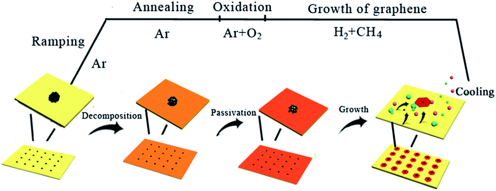
Graphene is considered as the candidate material for next-generation electronics and optoelectronics due to its superior physical properties.1–4 Among the various approaches for graphene fabrication, chemical vapor deposition (CVD) is considered as one of the most promising synthetic methods due to its scalability, uniformity and high quality.5–7 However, most CVD-grown graphene films cannot reach 100% coverage.8 The films exhibit polycrystalline structures with high-density grain boundaries on the substrates, which leads to highly unstable electronic properties, low charge carrier mobility and poor mechanical properties.9,10 Thus, it is desirable to prepare large-size single-crystalline graphene for building electronic devices with uniform properties.11 Earlier works demonstrate that the surface features of Cu foil, such as wrinkles, particles, steps and point defects, play an important role in the nucleation and growth of graphene.12–14 Many efforts have been made to alleviate the influence from the copper surface, such as mechanical polishing, electropolishing, longtime annealing at high temperature and high pressure, and resolidifying copper.13,15–17 By finely tuning the gas flow and flatting the surface, the size of the graphene domain has been successfully adjusted from the typical size of a few micrometers to millimeter-scale. Further improvement was also achieved by special treatment of the Cu foil. By changing the H2 protection gas to Ar atmosphere during the annealing process, the nucleation density can be greatly reduced, and hence submillimeter-sized single-crystalline graphene can be obtained.18 By further oxidizing the Cu surface using O-rich Cu foil or by introducing a small amount of O2 flow before the growth process, Ruoff et al. reported the first growth of centimeter-scale single-crystalline graphene, which is of great significance for industrial applications.19 Subsequently, by employing modified Cu–Ni alloy as a catalyst substrate and providing the carbon source in a localized area, Xie et al. successfully fabricated inch-scale single-crystalline graphene, which is the largest single-crystalline graphene fabricated to date.20 On the other hand, some attempts have also been made to build special growth architectures. It has been demonstrated that the nucleation density can be reduced by narrowing the growing space with a significant suppression of Cu evaporation.21,22 Liu et al. reported a 100 times increase in the growth rate with a very close space between Cu and substrate.23 Although various single-crystalline graphene films have been fabricated, the related device applications are still quite limited due to the difficulty of the transfer process and the randomly distributed graphene domains. Graphene-based devices should be fabricated by making special electrodes only on the randomly distributed graphene domains, which requires complex equipment and procedures.24,25 During the development of another similar material, carbon nanotubes (CNTs), an important strategy is to grow the CNTs in localized positions or in arrays.26,27 Thus, high-quality CNT-based devices can be easily manufactured with uniform performance and low cost. Thus, it is quite significant to develop similar technologies to grow single-crystalline graphene at designated position. To date, few efforts have been made for this purpose. It was reported that as-grown graphene domains on liquid substrates exhibit self-arrangement ability with closely packed hexagonal arrangement.28,29 To further realize the growth of graphene at the designated position, Yu et al. used electron beam lithographically to prepare patterned arrays of poly(methyl methacrylate) (PMMA) on Cu foils, which acted as pre-embedded nucleation centers. Hence, single-crystalline graphene arrays could be prepared at pre-patterned sites using the traditional CVD process.30,31 Andrew M. H. Ng et al. also reported the fabrication of periodic graphene arrays by nanoimprint lithography, which can be used in microelectrode array sensors.32 However, the current achievements, especially at designated position, require complex apparatuses and procedures, and the resulting single-crystalline graphene is as small as micrometer-sized, which is not suitable for building graphene devices for practical applications on a large scale.Herein, a simple and novel method is proposed to fabricate controllable, single-crystalline graphene with sub-millimeter size by employing a commercial printer to create nucleation patterns on Cu foil, as illustrated in Fig. 1. The commercial printer was employed to print carbon precursor dots on the Cu foil with a designed pattern that can be easily modified by computer software. The carbon precursor will be decomposed into carbon-rich dots on the Cu surface, which can serve as the nucleation centers in the following CVD process. According to the Lifshitz–Slyozov–Wagner (LSW) theory,33,34 the carbon-rich dots continuously absorb the carbon adatoms originating from the decomposition of CH4. Thus, single-crystalline graphene arrays can be formed at the designated position. As it is quite easy to obtain carbon dots on Cu foil using a commercial printing apparatus, this method provides a simple and efficient route to fabricate single-crystalline graphene arrays on a large scale.
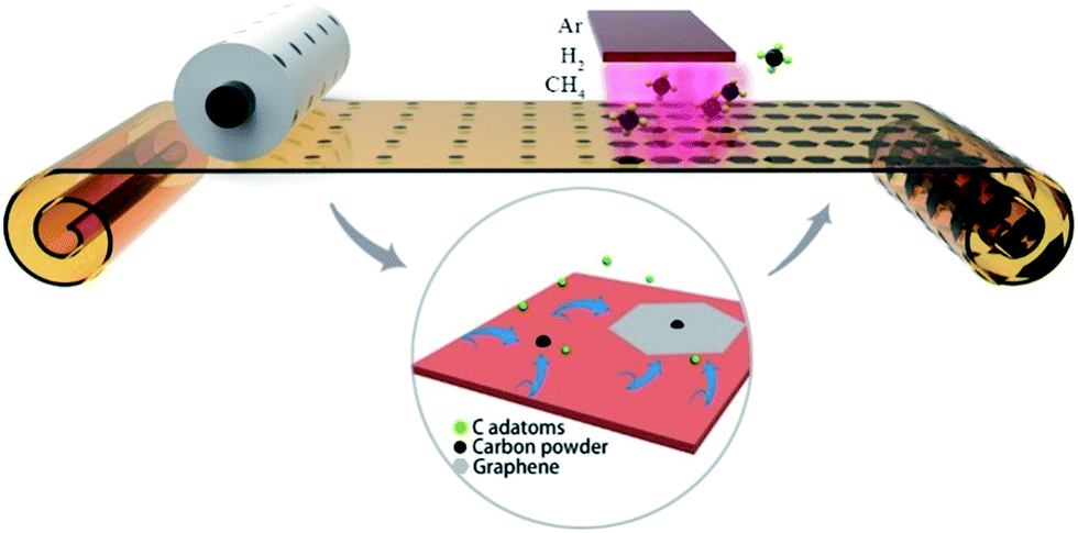 | ||
| Fig. 1 Schematic of the fabrication of single-crystalline graphene arrays. | ||
Experimental
CVD growth of graphene
Cu foils (46 μm-thick, 99.8%) with sizes of 21 cm × 29.7 cm were placed into a commercial laser or inkjet printer as normal, and the precursor pattern was designed using Photoshop with different pixel (px) arrays and then printed. Subsequently, the sample was positioned in the quartz tube furnace (diameter = 13 inches). Then, a CVD process for fabricating a graphene film was carried out, as illustrated in Fig. S1a in the ESI.† As a typical process, the chamber was heated to 1045 °C within 80 min under vacuum with the continuous input of 100 sccm Ar. The sample was then annealed at 1045 °C for 35 min with different atmospheres. Next, the graphene domain grew under the flow of 8 sccm diluted CH4 (1% CH4 in Ar) and 100 sccm pure H2 for 50 min. Finally, the system was cooled to room temperature while maintaining the gas flow. The detailed parameters are presented in Fig. S1b in the ESI.†Transfer of graphene arrays to the target substrates
The single-crystalline graphene arrays on Cu foil were transferred onto 300 nm SiO2/Si substrates and transmission electron microscopy (TEM) grids using the polymer assisted transferring method. A thin layer of PMMA (MicroChem 950 PMMA C, 10% in chloroform) was spin-coated on the as-synthesized sample at 3000 rpm for 1 min. The other side of the sample without PMMA was washed by NH4S2O8 (0.1 g ml−1) for 5 min. Subsequently, the sample was placed in an aqueous solution of NH4S2O8 (0.1 g ml−1) for about 4 h to completely remove the Cu foil. Then, the graphene with PMMA coating was washed several times by DI water. Finally, PMMA/graphene was delivered onto the target substrates, and the PMMA was then removed by acetone for 24 h.Characterization
Optical images were collected by a Leica optical microscope and mobile phone (Meizu MX4). The Raman spectra of the materials were recorded using a Renishaw inVia Reflex Raman Spectrometer with 532 nm-wavelength laser. The transferred graphene samples were characterized by field emission scanning electron microscopy (FE-SEM, Hitachi S-4800). TEM images were obtained by an aberration-corrected high-resolution transmission electron microscope (FEI Tecnai G2 F20) at an operating voltage of 200 kV.Results and discussion
Fig. 2a presents an optical image of the as-obtained graphene arrays on Cu foil after the laser printing-assisted CVD process. After oxidation treatment at 200 °C in atmospheric environment, ordered and homogenous bright spot arrays with sizes of 2 × 2 cm2 can be clearly observed due to the obvious contrast. As shown in Fig. 2b, at larger magnification, 5 × 5 bright spot arrays can be observed in the area of 3 × 3 mm2. Each spot is hexagonal in shape, 400 μm from side to side, and 450 μm across the corners. The distances between the centers of neighboring spots are about 0.5 mm, which is the same as the period of the original carbon precursors. Surprisingly, in contrast to the random growth of graphene domains, the bright spots in this case arrange orderly and are nearly parallel, as marked by the blue line in Fig. 2b. This suggests that the bright spots had similar orientations and growth rates during the CVD process, which were difficult to control in other works. It should be noted that there are obvious black dots at the center of each bright spot. The black dots are carbon-rich dots embedded by the laser printing method. However, after the CVD process, the black dots are larger in diameter than the original printed carbon precursor due to decomposition and diffusion during the CVD process (see Fig. S2 in ESI†). After transferring the bright spots onto an Si/SiO2 substrate, ordered arrays can also be obtained, as shown in the SEM image in Fig. 2c. However, the centers of these arrays on the Si/SiO2 substrate seem broken and have some impurities after the transferring process.35 This might be due to the drastic etching and rough surfaces on the centers (see Fig. S3 in ESI†). At the edge of a randomly related graphene domain, the SEM image in Fig. 2d presents a flat surface with uniform contrast, suggesting a monolayer structure. This can be confirmed by the Raman characterization in Fig. 2e, which resembles the standard spectrum of monolayer graphene. The I2D/IG intensity ratio is about 4.8, which is much larger than 2, and the full width at half maximum of the 2D peak is about 29.5 cm−1. Furthermore, the disorder-induced D peak at 1350 cm−1 is hardly detected on the selected graphene domain, indicating the high quality of the graphene film in this area. The Raman mapping result in Fig. 2f confirms the monolayer nature over one corner of the as-obtained single-crystalline graphene domain.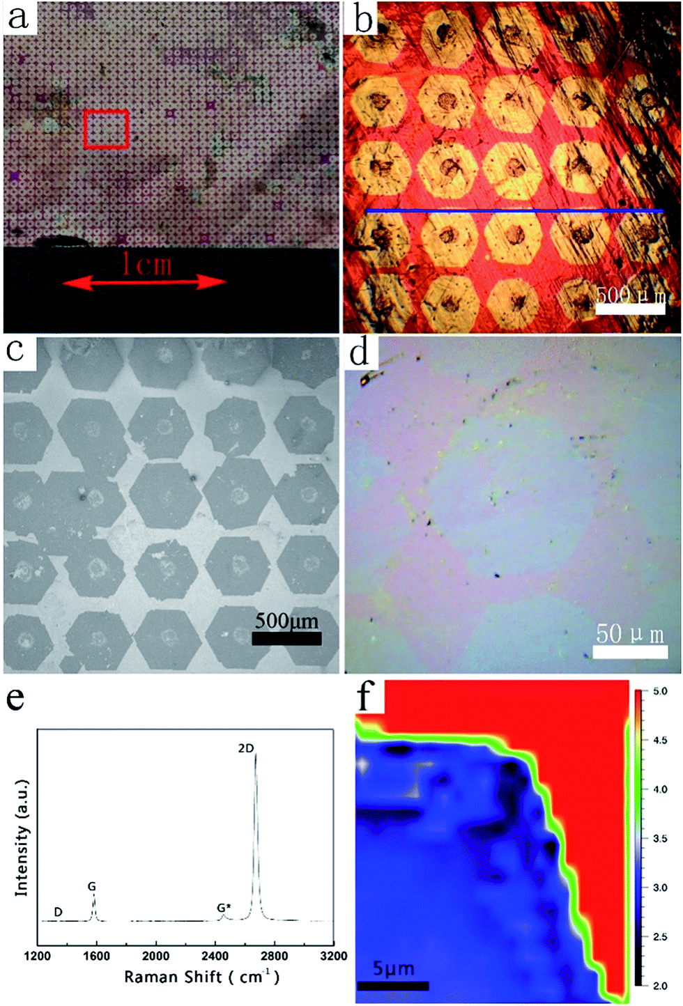 | ||
| Fig. 2 (a) Optical image and (b) microscope image of single-crystalline graphene arrays; (c) SEM image and (d) microscope image of single-crystalline graphene arrays on Si/SiO2 substrates; (e) Raman spectrum and (f) corresponding Raman mapping of one corner of a single-crystalline graphene domain. | ||
TEM and selective area electron diffraction (SAED) were further used to characterize the submillimeter-sized graphene domains that were transferred onto the amorphous carbon-covered TEM grid, as shown in the SEM image in Fig. 3a. Fig. 3b clearly shows a typical graphene domain from Fig. 3a, which has a perfect hexagonal shape with a size of around 350 μm. Careful observation reveals obvious breaks in the middle of graphene, which may be caused by the transferring process, similar to the phenomenon observed in the Si/SiO2 sample. Fig. 3c, taken in the area highlighted with the yellow frame in Fig. 3b, demonstrates the same edge structures observed by SEM. The regular geometry of the hexagon with nearly 120° angles suggests that it is single-crystalline in nature. SAED measurements were performed on 14 individual regions across the whole graphene domain to determine the crystallinity. Fig. 3d–h show five typical SAED patterns taken at the areas labeled in Fig. 3b. The sharp and bright spots in all the SAED patterns fit the typical hexagonal structure and are consistent with previous reports.36 The difference in relative angle of the graphene SAED patterns of the 14 areas is less than 2°, suggesting the single-crystal nature of this graphene flake with a size of over 350 μm (see Fig. S4 in ESI†). The results of quantitative intensity analysis of one typical diffraction spot along the line illustrated in Fig. 3e are given in Fig. 3i. The intensity of the inner rings is always higher than that of the outer ones, which indicates that the graphene domain is a monolayer.36,37
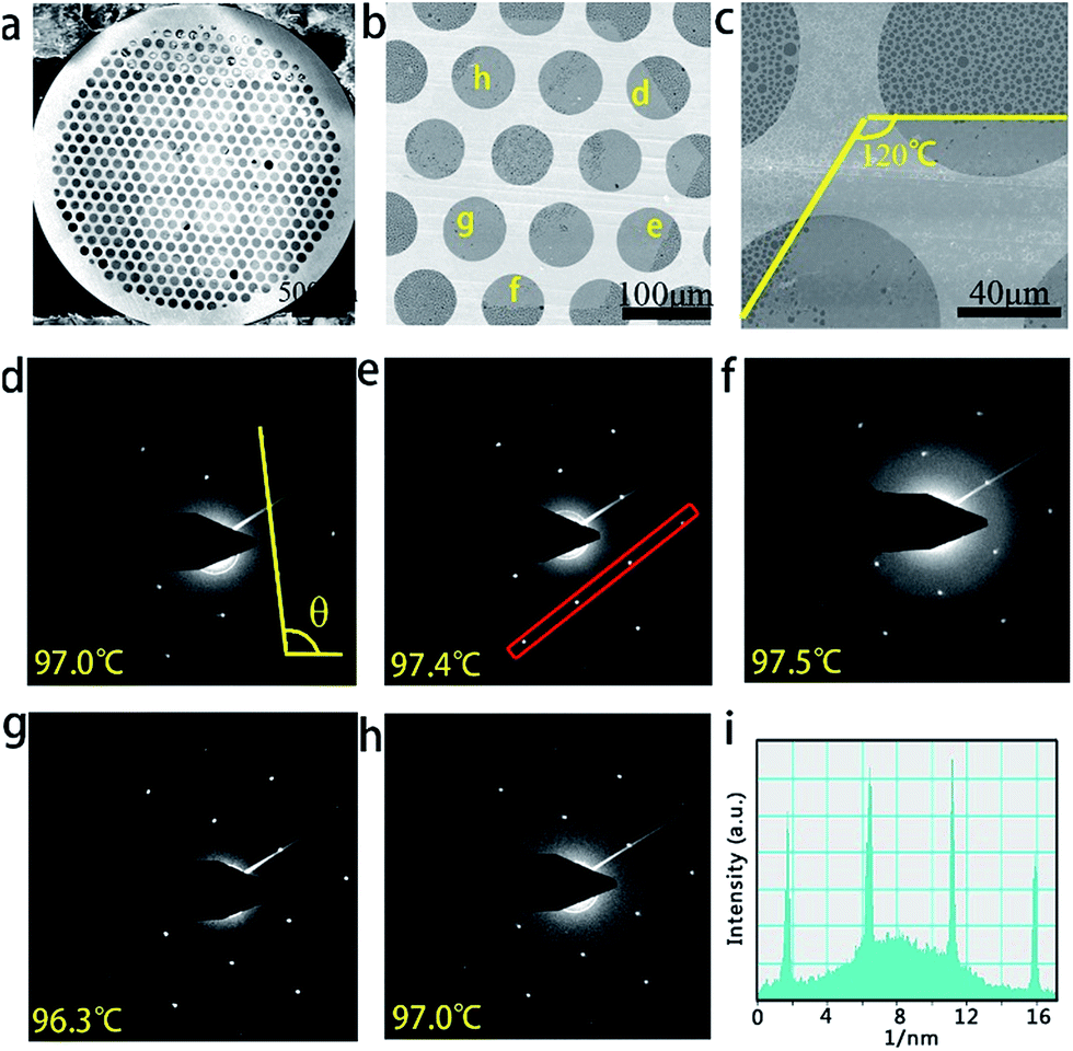 | ||
| Fig. 3 (a–c) SEM images of graphene domains transferred on an amorphous carbon-covered TEM grid at different magnifications; (d–h) selected area electron diffraction (SEAD) data on the selected locations as marked in (b); (i) intensity profile along the line in (e). | ||
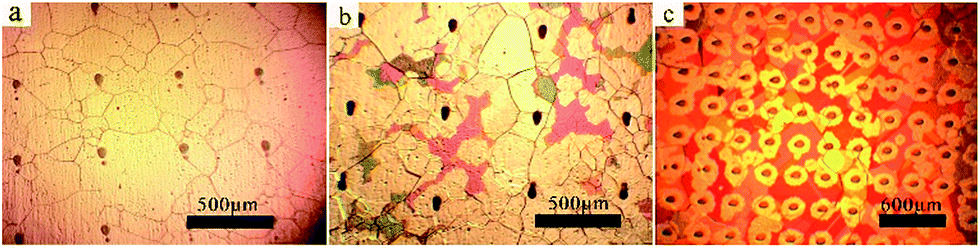
The formation of submillimeter-sized single-crystalline graphene arrays has been studied in detail. Fig. 4 compares the surface morphologies of graphene domains on Cu foils after the CVD process under different atmospheres and with different pre-embedded printing dots with periods of 0.5 mm, as illustrated in Fig. S1 in the ESI.† It is well-known that H2 is widely used as the reducing atmosphere before the growth of graphene to remove the native copper oxide on the raw Cu foil. In this work, under the reducing atmosphere with H2 during the annealing process, the graphene domains grow randomly with sizes of less than 100 μm without pre-embedding printing precursors (Fig. 4a). After printing 1- and 4-px precursors (Fig. 4b and c), the graphene domains become denser to form a closed film but are still randomly distributed on the surface. Upon careful observation, the dark centers in graphene domains turn to be disappeared in the 1-px sample and very light in the 4-px sample. Comparing the different precursors just after annealing before the CVD growth process indicates that the precursors can survive the annealing process, as shown in Fig. S5 in the ESI.† As discussed in other reports,38 H2 plays two roles: promoting the decomposition of CH4 and etching carbon. Herein, the long-term exposure to H2 during the CVD process could etch away the printed precursor, which is mainly composed of carbon (see Fig. S2 in ESI†). When the reducing H2 atmosphere is changed to a pure Ar atmosphere, the graphene domains are still randomly distributed on the Cu foil without the help of pre-printed precursors, as shown in Fig. 4d. However, compared to the passivation of oxidation on Cu as same as other reports, there are no obvious morphology changes, and the precursors also disappear after the CVD process in sample with 1-px precursors (Fig. 4e). Upon further enlarging the precursor size to 4-px, graphene domains appear on the pre-designed location with darker nucleation centers. However, some graphene domains also grow in the gaps between nucleation centers. To further study the influence of O2, a given mass of O2 atmosphere was added by introducing air during the annealing process and stopped before the growth of graphene. As shown in Fig. 4g, the nucleation density of the graphene domains is further decreased, and the size of single-crystalline graphene domains reaches around 400 μm. Similar to the phenomenon observed under Ar atmosphere, the 1-px precursors could not survive after long-time CVD process, and random graphene domains are formed, as shown in Fig. 4h. Finally, with the help of both O2 atmosphere and 4-px precursors, submillimeter-sized single-crystal graphene arrays are obtained in Fig. 4i.
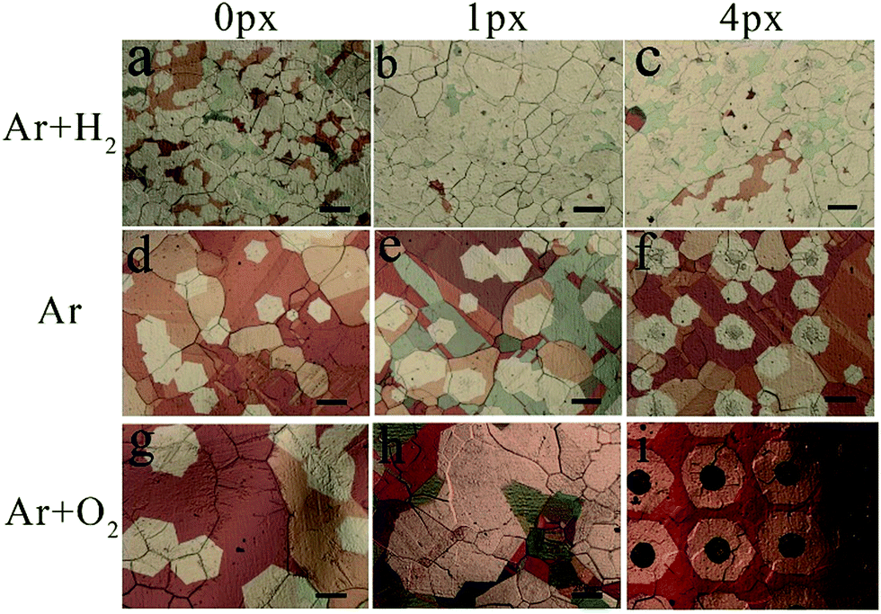 | ||
| Fig. 4 Optical images of graphene domains on Cu foil with different pre-printed precursor dots at different annealing atmospheres (scale bar in all pictures is 200 μm). | ||
Based on the above results, Fig. 5 illustrates the possible mechanism and morphological evolution during the entire CVD process. It is known that most of the carbon toner consists of mostly carbon precursor and some magnetic materials such as Fe-based particles, as demonstrated in Fig. S2 in the ESI.† During the heat ramping process under pure Ar atmosphere, the printed precursors decompose and diffuse to form microsized particles on the Cu surface, which are a little larger than the original precursor dots. It has to be mentioned that the existence of H2 and O2 could etch away the nucleation centers if the carbon precursor is not sufficient. With the introduction of the 4-px precursor, the carbon precursor survived after the annealing process with a certain amount of oxygen. The introduction of oxygen in the annealing process could slightly oxidize the Cu foil to form a passivation layer, which has been demonstrated to be very useful for reducing the nucleation density of graphene.19 According to LSW theory, the stable carbon precursors would serve as the nucleation centers to grow the graphene domains by absorbing the carbon adatoms originating from the decomposition of CH4 if the nucleation density is lower than the period of precursor. Otherwise, in addition to the graphene domains at the pre-designed locations, some graphene domains would grow at the gaps between the precursor dots if the nucleation density is higher than the period of the precursors, as demonstrated in Fig. 5f. Finally, it can be concluded that the successful growth of millimeter-sized single-crystalline graphene arrays has two requirements: (1) enough carbon precursors should be provided that can serve as the nucleation centers and survive during the annealing process, and (2) a suitable oxygen atmosphere is required to form the passivation layer on the Cu foil, which results in a lower nucleation density compared to the density of the pre-printed precursors.
 | ||
| Fig. 5 Schematic of the possible mechanism and morphological evolution for the formation of single-crystalline graphene arrays by CVD. | ||
In addition, as one of the commonly used printing technologies, an inkjet printer was also used to embed the precursor dots on the Cu foil. In contrast to laser printing, the precursor dots printed by inkjet printer could not survive under the Ar and O2 atmosphere as above, possibly due to the quite different composition of the ink. Upon further study, it is found that the ink precursor could be maintained under H2 atmosphere. As shown in Fig. 6a and b, random graphene domains are formed with sizes of less than 100 μm if H2 protection is required during the annealing process. According to the analysis above, the annealing process under H2 atmosphere could lead to high nucleation density, resulting in the formation of graphene domains in the gaps between precursors. As an alternative method, if the period of the inkjet printer is changed to 300 μm, the graphene arrays can also be obtained under the same CVD process. This result confirms that there are two necessary requirements, as mentioned above, to form single-crystalline graphene arrays.
 | ||
| Fig. 6 Microscope images of (a) inkjet printing precursor dots on Cu foil, (b) as-grown graphene domains under Ar + O2 annealing atmosphere, and (c) as-grown single-crystalline graphene arrays under H2 annealing atmosphere. | ||
Conclusions
In summary, a novel commercial printing-assisted CVD method was successfully developed to fabricate well-distributed submillimeter-sized single-crystalline graphene arrays. The detailed mechanism has been carefully studied to reveal the essential requirements for the formation of single-crystalline graphene arrays. This work provides a facile strategy for the scalable fabrication of single-crystalline graphene arrays, which is essential for the exploration of graphene-based electronic devices.Acknowledgements
This work is supported by the National Natural Science Foundation of China (51402322), and Science Technology Department of Zhejiang Province (2015C01003).Notes and references
- K. S. Novoselov, A. K. Geim, S. V. Morozov, D. Jiang, Y. Zhang, S. V. Dubonos, I. V. Grigorieva and A. A. Firsov, Science, 2004, 306, 666 CrossRef CAS PubMed.
- T. R. O. Graphene, Eur. J. Org. Chem., 2002, 2003, 82–91 Search PubMed.
- A. K. Geim, Science, 2009, 324, 1530 CrossRef CAS PubMed.
- R. K. Joshi, S. Alwarappan, M. Yoshimura, V. Sahajwalla and Y. Nishina, Applied Materials Today, 2015, 1, 1–12 CrossRef.
- S. Bae, H. Kim, Y. Lee, X. Xu, J. S. Park, Y. Zheng, J. Balakrishnan, T. Lei, H. R. Kim, Y. I. Song, Y. J. Kim, K. S. Kim, B. Ozyilmaz, J. H. Ahn, B. H. Hong and S. Iijima, Nat. Nanotechnol., 2010, 5, 574–578 CrossRef CAS PubMed.
- K. S. Kim, Y. Zhao, H. Jang, S. Y. Lee, J. M. Kim, K. S. Kim, J. H. Ahn, P. Kim, J. Y. Choi and B. H. Hong, Nature, 2009, 457, 706–710 CrossRef CAS PubMed.
- Y. Zhang, L. Zhang and C. Zhou, Acc. Chem. Res., 2013, 46, 2329 CrossRef CAS PubMed.
- A. Ambrosi, A. Bonanni, Z. Sofer and M. Pumera, Nanoscale, 2013, 5, 2379 RSC.
- P. Y. Huang, C. S. Ruiz-Vargas, A. M. van der Zande, W. S. Whitney, M. P. Levendorf, J. W. Kevek, S. Garg, J. S. Alden, C. J. Hustedt, Y. Zhu, J. Park, P. L. McEuen and D. A. Muller, Nature, 2011, 469, 389–392 CrossRef CAS PubMed.
- L. A. Jauregui, H. Cao, W. Wu, Q. Yu and Y. P. Chen, Solid State Commun., 2011, 151, 1100–1104 CrossRef CAS.
- D. Geng, B. Wu, Y. Guo, L. Huang, Y. Xue, J. Chen, G. Yu, L. Jiang, W. Hu and Y. Liu, Proc. Natl. Acad. Sci. U. S. A., 2012, 109, 7992–7996 CrossRef CAS PubMed.
- D. L. Duong, G. H. Han, S. M. Lee, F. Gunes, E. S. Kim, S. T. Kim, H. Kim, Q. H. Ta, K. P. So, S. J. Yoon, S. J. Chae, Y. W. Jo, M. H. Park, S. H. Chae, S. C. Lim, J. Y. Choi and Y. H. Lee, Nature, 2012, 490, 235–239 CrossRef CAS PubMed.
- B. Wang, H.-R. Zhang, Y.-H. Zhang, Z.-Y. Chen, Z. Jin, X.-Y. Liu, L.-Z. Hu and G.-H. Yu, Mater. Lett., 2014, 131, 138–140 CrossRef CAS.
- B. Wang, Y. Zhang, H. Zhang, Z. Chen, X. Xie, Y. Sui, X. Li, G. Yu, L. Hu, Z. Jin and X. Liu, Carbon, 2014, 70, 75–80 CrossRef CAS.
- A. Mohsin, L. Liu, P. Liu, W. Deng, I. N. Ivanov, G. Li, O. E. Dyck, G. Duscher, J. R. Dunlap and K. Xiao, ACS Nano, 2013, 7, 8924–8931 CrossRef CAS PubMed.
- Z. Yan, J. Lin, Z. Peng, Z. Sun, Y. Zhu, L. Li, C. Xiang, E. L. Samuel, C. Kittrell and J. M. Tour, ACS Nano, 2013, 7, 875 CrossRef CAS.
- H. Wang, G. Wang, P. Bao, S. Yang, W. Zhu, X. Xie and W. J. Zhang, J. Am. Chem. Soc., 2012, 134, 3627–3630 CrossRef CAS PubMed.
- H. Zhou, W. J. Yu, L. Liu, R. Cheng, Y. Chen, X. Huang, Y. Liu, Y. Wang, Y. Huang and X. Duan, Nat. Commun., 2013, 4, 2096 Search PubMed.
- Y. Hao, M. S. Bharathi, L. Wang, Y. Liu, H. Chen, S. Nie, X. Wang, H. Chou, C. Tan, B. Fallahazad, H. Ramanarayan, C. W. Magnuson, E. Tutuc, B. I. Yakobson, K. F. McCarty, Y. W. Zhang, P. Kim, J. Hone, L. Colombo and R. S. Ruoff, Science, 2013, 342, 720–723 CrossRef CAS PubMed.
- T. Wu, X. Zhang, Q. Yuan, J. Xue, G. Lu, Z. Liu, H. Wang, H. Wang, F. Ding, Q. Yu, X. Xie and M. Jiang, Nat. Mater., 2016, 15, 43–47 CrossRef CAS PubMed.
- S. Chen, H. Ji, H. Chou, Q. Li, H. Li, J. W. Suk, R. Piner, L. Liao, W. Cai and R. S. Ruoff, Adv. Mater., 2013, 25, 2062–2065 CrossRef CAS PubMed.
- C. Wang, W. Chen, C. Han, G. Wang, B. Tang, C. Tang, Y. Wang, W. Zou, W. Chen, X. A. Zhang, S. Qin, S. Chang and L. Wang, Sci. Rep., 2014, 4, 4537 Search PubMed.
- X. Xu, Z. Zhang, L. Qiu, J. Zhuang, L. Zhang, H. Wang, C. Liao, H. Song, R. Qiao, P. Gao, Z. Hu, L. Liao, Z. Liao, D. Yu, E. Wang, F. Ding, H. Peng and K. Liu, Nat. Nanotechnol., 2016, 11, 930–935 CrossRef CAS PubMed.
- D. Ding, P. Solis-Fernandez, H. Hibino and H. Ago, ACS Nano, 2016, 10, 11196–11204 CrossRef CAS PubMed.
- K. Jo, S.-M. Kim, S.-M. Lee, J.-H. Kim, H.-J. Lee, K. S. Kim, Y. D. Kwon and K.-S. Kim, Carbon, 2015, 82, 168–175 CrossRef CAS.
- B. J. Hinds, N. Chopra, T. Rantell, R. Andrews, V. Gavalas and L. G. Bachas, Science, 2004, 303, 62–65 CrossRef CAS PubMed.
- M. Engel, J. P. Small, M. Steiner, M. Freitag, A. A. Green, M. C. Hersam and P. Avouris, ACS Nano, 2009, 2, 2445–2452 CrossRef PubMed.
- D. Geng, B. Luo, J. Xu, Y. Guo, B. Wu, W. Hu, Y. Liu and G. Yu, Adv. Funct. Mater., 2014, 24, 1664–1670 CrossRef CAS.
- M. Zeng, L. Wang, J. Liu, T. Zhang, H. Xue, Y. Xiao, Z. Qin and L. Fu, J. Am. Chem. Soc., 2016, 138, 7812–7815 CrossRef CAS PubMed.
- W. Wu, L. A. Jauregui, Z. Su, Z. Liu, J. Bao, Y. P. Chen and Q. Yu, Adv. Mater., 2011, 23, 4898–4903 CrossRef CAS PubMed.
- Q. Yu, L. A. Jauregui, W. Wu, R. Colby, J. Tian, Z. Su, H. Cao, Z. Liu, D. Pandey, D. Wei, T. F. Chung, P. Peng, N. P. Guisinger, E. A. Stach, J. Bao, S. S. Pei and Y. P. Chen, Nat. Mater., 2011, 10, 443–449 CrossRef CAS PubMed.
- A. M. H. Ng, Y. Wang, W. C. Lee, C. T. Lim, K. P. Loh and H. Y. Low, Carbon, 2014, 67, 390–397 CrossRef CAS.
- I. M. Lifshitz and V. V. Slyozov, J. Phys. Chem. Solids, 1961, 19, 35–50 CrossRef.
- C. Wagner, Bunsen-Ges. Phys. Chem., Ber., 1961, 65, 581–591 CAS.
- A. Ambrosi and M. Pumera, Nanoscale, 2014, 6, 472 RSC.
- Z. Z. Sun, A. R. O. Raji, Y. Y. Zhu, C. S. Xiang, Z. Yan, C. Kittrell, E. L. G. Samuel and J. M. Tour, ACS Nano, 2012, 6, 9790–9796 CrossRef CAS PubMed.
- S. Horiuchi, T. Gotou, M. Fujiwara, R. Sotoaka, M. Hirata, K. Kimoto, T. Asaka, T. Yokosawa, Y. Matsui and K. Watanabe, Jpn. J. Appl. Phys., 2003, 42, 1073 CrossRef.
- I. Vlassiouk, M. Regmi, P. Fulvio, S. Dai, P. Datskos, G. Eres and S. Smirnov, ACS Nano, 2011, 5, 6069 CrossRef CAS PubMed.
Footnote |
| † Electronic supplementary information (ESI) available. See DOI: 10.1039/c7ra01947e |
| This journal is © The Royal Society of Chemistry 2017 |