
 Open Access Article
 This Open Access Article is licensed under a
 Creative Commons Attribution 3.0 Unported Licence
Abnormal gas pressure sensitivity of the visible emission in ZnO quantum dots prepared by improved sol–gel method: the role of surface polarity
Xiaoman Maa,
Honggang Ye *ab,
Xiangyang Duana,
Chu Lia,
Gaoming Lia and
Shijie Xub
*ab,
Xiangyang Duana,
Chu Lia,
Gaoming Lia and
Shijie Xub
aDepartment of Applied Physics, MOE Key Laboratory for Nonequilibrium Synthesis and Modulation of Condensed Matter, Xi'an Jiaotong University, Xi'an, 710049, People's Republic of China. E-mail: hgye@mail.xjtu.edu.cn
bDepartment of Physics, Shenzhen Institute of Research and Innovation (SIRI), The University of Hong Kong, Pokfulam Road, Hong Kong, People's Republic of China
First published on 9th June 2017
Abstract
ZnO quantum dots (QDs) were prepared with an improved sol–gel approach. In addition to the sensitive response to ambient gas types, the visible emission of ZnO QDs is found to be sensitively dependent on the gas pressure. For example, the fluorescence intensity decreases significantly with decreasing air pressure, and even almost completely quenches at 10 mbar. This is a striking phenomenon which is opposed in the case of ZnO nanowires (NWs), for which the visible fluorescence is enhanced in a vacuum condition. A consistent model is proposed to explain the phenomenon, in which the polar surface induced band bending in ZnO QDs could be significantly compensated by that induced by oxygen adsorption, while such a compensation effect is negligibly small in NWs with long lengths along the c-axis. The central part of the model emphasizes that the wurtzite ZnO QDs may not be simply seen as isotropic spheres, but a polar surface charging effect may form the base of the gas sensitivity.
Owing to the wide band gap (i.e., ∼3.37 eV at 300 K) and large exciton binding energy (60 meV), as well as many other outstanding properties, bulk ZnO and nanostructures of ZnO have attracted a great deal of interest for potential applications in the fields of optoelectronic devices, photocatalysts, gas sensor, and biological labels.1–11 As one of the typical nanostructures, ZnO quantum dots (QDs) have unique physical properties due to their strong quantum size effect and surface effect.12–17 The photoluminescence (PL) spectrum of ZnO QDs usually features two emission bands, a relatively narrow ultraviolet (UV) emission from the band-edge excitonic recombination, and a broad visible emission induced by defects. The relative intensity of the two emission bands depends greatly on the crystal quality and ambient conditions.17,18 The efficient broad visible emission of ZnO QDs makes them a promising candidate material for phosphors.19 Compared with conventional rare earth phosphors, ZnO QDs are less toxic, cheaper and easily acquired. The less-toxic property, resulting from the lack of cadmium, also makes ZnO QDs very appealing in biological applications such as fluorescence labeling and drug delivery.20,21 Due to the atmosphere sensitivity, on the other hand, ZnO QDs can be used as gas sensors with a high sensitivity, particularly for some toxic gases such as NO2, NH3, etc.8–10,22
Moreover, it has been found that the visible emission intensity of ZnO QDs also shows a significant dependence on gas pressure, especially the partial pressure of oxygen. For instance, the visible emission decreases remarkably with decreasing air pressure.23,24 However, a unified and self-convincing model for the mechanism causing the phenomenon has not yet been established so far. It is noteworthy that the phenomenon in ZnO QDs is even contrary to the case of ZnO nanowires (NWs) (or nanorods), for which the visible emission intensity increases after oxygen desorption.25 The atmosphere sensitivity is usually attributed to the adsorption of oxygen molecules, which can induce a depletion layer in the near surface region of ZnO nanostructures by capturing electrons from ZnO. The electron–hole pairs in this region will be spatially separated immediately after generation, resulting in a weak fluorescence. The existence of other gases in the ambient condition influences the coverage of O2 on the ZnO surface and then leads to an indirect response in PL intensity.10,22,26 This model applies to ZnO NWs and other semiconductors, such as TiO2.27 However, it seems inapplicable to the abnormal result of ZnO QDs. Some ideas have been suggested in the literature to illustrate the abnormal phenomenon. M. Ghosh et al.24,28 suggested that the visible luminescence is from  and
and  and the upward band bending induced by oxygen adsorption facilitates the formation of these positively charged defects, so the visible PL intensity is proportional to the ambient oxygen partial pressure. For ZnO nanoparticles (NPs), a broad visible emission was specified by Gheisi et al.29 to oxygen interstitials, and the intensity increase with oxygen adsorption was attributed to aggregation of holes in the edge of the depletion layer. Regardless of the controversy and validity of these ideas, all of them follow the band bending model for ZnO NWs, so no one can illustrate the contrary phenomenon between ZnO NWs (or nanorods) and QDs (or NPs). In this article, we try to solve this problem by conducting a systematic study on ZnO NWs and QDs. Based on the experimental data and first-principles calculations, we propose that the oxygen molecules preferably adsorb on the Zn-terminated (0001) polar surface of QDs and there is compensation between the polar surface and the oxygen adsorption induced band bending. However, such a compensation effect is negligible in ZnO NWs since oxygen adsorption predominately occurs on the non-polar surfaces, such as m-planes.
The ZnO QDs were prepared by an improved sol–gel technique by using zinc acetate dihydrate [(Zn(CH3COO)2·2H2O), 99.9%] and lithium hydroxide monohydrate (LiOH·H2O) as the original materials. The process is similar to that reported by Spanhel and Anderson.30 10 mL of 0.05 mol L−1 zinc acetate solution was prepared as a precursor. The synthesis reaction started with the dropwise addition of LiOH alcohol solution (10 mL of 0.1 mol L−1 LiOH) into the precursor. After that, ZnO QDs were carried out from the transparent sol by centrifugation and then washed several times to remove the excess acetate and lithium ions. Finally, the obtained QDs in an alcohol solution were transferred onto a sapphire substrate by a spin-coating method. The ZnO NWs were also synthesized by a hydrothermal method. The source materials are zinc acetate dihydrate and hexamethylenetetramine (HMT, 99.9%). The precursor solution was prepared by using equal molar zinc acetate and HMT (0.05 mol L−1, 100 mL). Subsequently, the precursor was heated up to 95 °C in a hydrothermal reactor in which a sapphire substrate was fixed. After maintaining for 6 hours, hexagonal ZnO NWs deposited on the sapphire substrate were obtained. A detailed synthesis process can be seen in ref. 31.
The crystal structure of the samples was characterized by using X-ray diffraction (XRD, Bruker Advance D8) with Cu Kα radiation (λ = 0.15406 nm). The microstructure was measured by using a transmission electron microscope (TEM, JEM-2100) operated at 200 kV, including high resolution electron microscopy (HRTEM). The morphology and microstructure of the NWs were characterized by scanning electron microscopy (SEM, JEOL-7800F). The PL spectra were obtained by using a spectrograph (QM40, produced by Photon Technology International) with the sample fixed in a gas pressure controllable vacuum cavity. The 325 nm laser line of a He–Cd laser (Kimmon) was used as the excitation source.
Shown in Fig. 1 are the microstructural characterization results of the samples studied in the present work. From Fig. 1(a), it can be seen that the QDs sporadically distribute on the sapphire substrate, with an approximately uniform size. The HRTEM images display that the ZnO QDs with an average particle size of about 5 nm are typically hexagonal faceted with a (10![[1 with combining macron]](https://www.rsc.org/images/entities/char_0031_0304.gif) 0) plane spacing of 0.277 nm and a (0002) plane spacing of 0.256 nm. The derived lattice constants are a = 3.195 Å and c = 5.121 Å, slightly smaller than those of bulk ZnO (a = 3.249 Å, c = 5.204 Å).4 As shown in Fig. 1(b) and (c), the synthesized ZnO NWs exhibit a hexagonal prism shape with an average length of about 2 μm and a diameter of about 70–80 nm. The XRD patterns in Fig. 1(d) indicate that the QDs and NWs crystallize in the wurtzite phase. The (0002) peak becomes dominant for the NW sample since the NWs have an approximately orderly arrangement.
0) plane spacing of 0.277 nm and a (0002) plane spacing of 0.256 nm. The derived lattice constants are a = 3.195 Å and c = 5.121 Å, slightly smaller than those of bulk ZnO (a = 3.249 Å, c = 5.204 Å).4 As shown in Fig. 1(b) and (c), the synthesized ZnO NWs exhibit a hexagonal prism shape with an average length of about 2 μm and a diameter of about 70–80 nm. The XRD patterns in Fig. 1(d) indicate that the QDs and NWs crystallize in the wurtzite phase. The (0002) peak becomes dominant for the NW sample since the NWs have an approximately orderly arrangement.
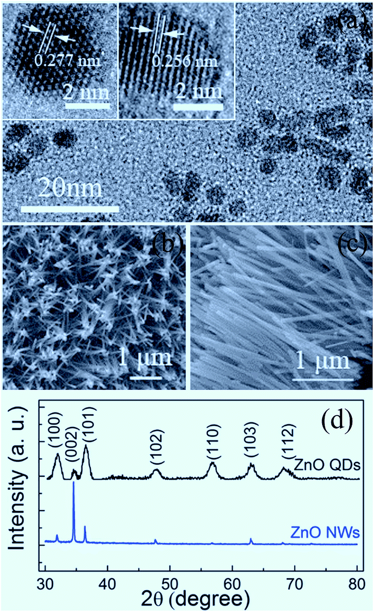 | ||
| Fig. 1 TEM and HRTEM images of ZnO QDs (a); SEM images of ZnO NWs (b and c); and XRD patterns of QDs and NWs (d). | ||
The room temperature PL spectra of the ZnO QDs and NWs under different air pressures are shown in Fig. 2. Each curve in this figure consists of a UV band and a broad visible band. The UV emission peaks are at 357 nm for QDs and at 385 nm for NWs. The difference might originate from the strong quantum size effect in QDs.17,32–34 The broad visible band, centered at 530 nm for both QDs and NWs, was suggested to be from near surface defects, such as oxygen vacancy or zinc interstice,19,35,36 but the microstructural origin is still debatable so far.37 Here we focus on the intensity variation of the broad visible emission with gas pressure. It can be seen from Fig. 2(a) that the peak center of the visible emission remains unchanged with air pressure, but the intensity decreases significantly with decreasing air pressure for ZnO QDs. When the pressure changes from normal atmospheric to 10 mbar (mb), the peak intensity of the visible emission reduces by about 88%, indicating the strong dependency of the visible emission on air pressure. The declining intensity slows when the air pressure is lower than 10 mb. As shown in Fig. 2(b), the intensity change of the visible emission for ZnO NWs is relatively small but it is noteworthy that the intensity increases with decreasing air pressure. This result for ZnO NWs is consistent with previous reports25 but opposite to the present results for the QDs. Because the NWs have a relative large diameter and small surface-to-volume ratio, the magnitude of the PL intensity variation is weaker than that of the QDs.
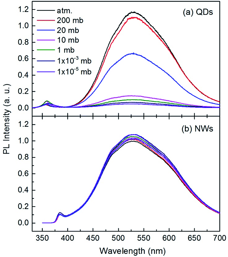 | ||
| Fig. 2 Room temperature PL spectra of the ZnO QDs (a) and NWs (b) under different air pressures. | ||
The phenomenon is also interestingly reversible. For example, when the air pressure is returned to a normal value, the luminescence intensity recovers immediately and completely. This process is clearly shown in Fig. 3. When a circular change of the ambient conditions was performed (from normal atmosphere to vacuum (10 mb), and return to the normal), the PL intensity at 530 nm exhibits a sharp contrast evolution for the NWs and QDs, e.g., a convex curve for the NWs but a concave curve for the QDs. This means that the variation in PL intensity may not be from internal changes or chemical reactions occurring in the near surface region since the changes are usually irreversible. Surface adsorption is thus the main factor responsible for the gas pressure sensitivity of PL intensity. The adsorption should not be very strong because the amount of adsorbed gas molecules depends greatly on the gas pressure.
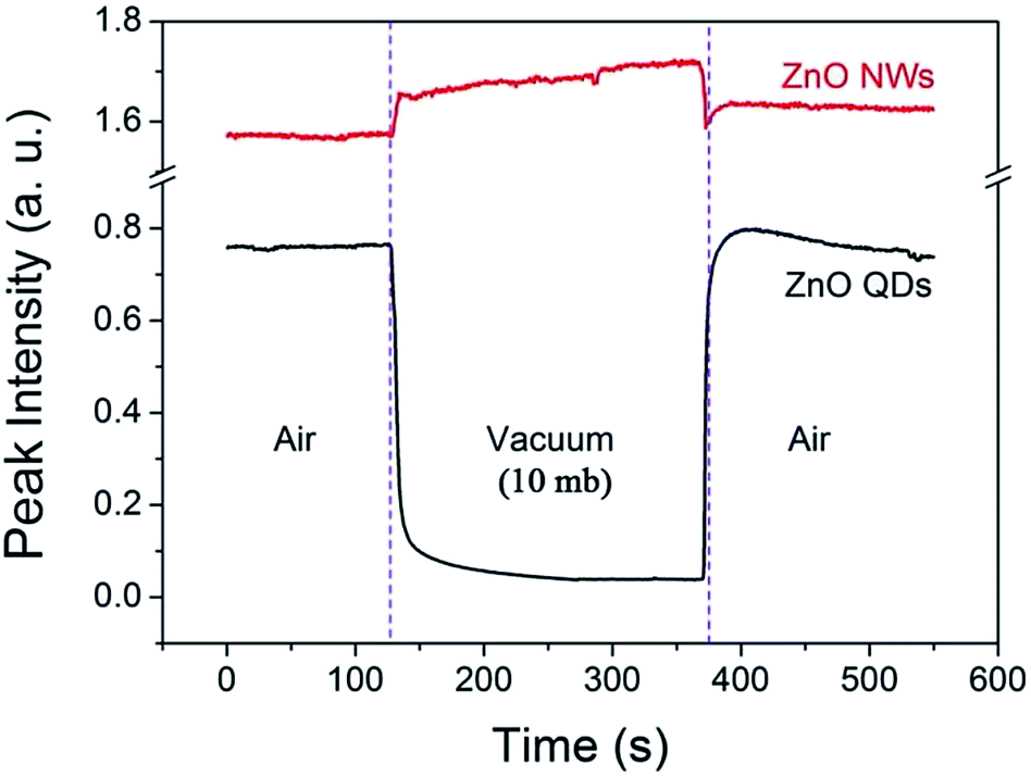 | ||
| Fig. 3 Variation of the visible emission intensity (monitored at 530 nm) of the ZnO QDs and NWs at room temperature in an atmosphere–vacuum–atmosphere cycle. | ||
To explore the origin of the abnormal gas pressure response of the visible emission of the ZnO QDs, the PL spectra of the QDs were registered under the pure gas circumstances of N2 and O2. The results are shown in Fig. 4, in which the three solid curves represent the PL spectra obtained under a normal atmospheric pressure for the different gases. Before refilling another type of gas, the sample chamber was mechanically pumped to a vacuum of 0.015 mb. Clearly, the pure O2 condition is favorable for the visible emission of the ZnO QDs. This means that oxygen could play a major role in affecting the visible emission of the ZnO QDs, which is consistent with the previous reports for ZnO NWs.8 As mentioned in the introduction part, the O2 molecules were supposed to be electron acceptors. They may capture an electron from ZnO and become O2−. In this way, the adsorbed O2 molecules form a negatively charged layer and then induce upward band bending in the near surface region of ZnO. The photo-generated electron–hole pairs in the depletion layer may be easily separated by the electric field, and thus reduce their radiative recombination rate, leading to a weaker emission intensity. That is just the sensitizing mechanism of the visible emission on the partial oxygen pressure for ZnO NWs. This model has been well accepted and even applies to other oxide semiconductors.27 Nevertheless, it seems not applicable for explaining the abnormal results of the ZnO QDs, for which a new physical model is required.
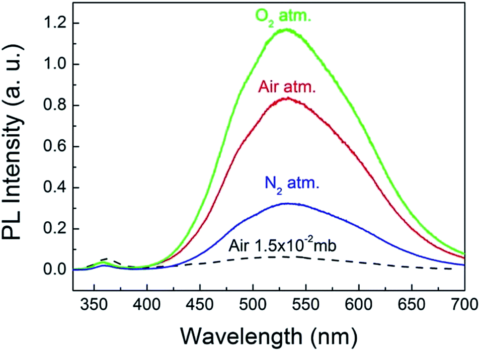 | ||
| Fig. 4 PL spectra of the ZnO QDs measured under a normal pressure of pure O2, N2 and atmospheric air. | ||
Examining the microstructural difference between ZnO NWs and QDs will be useful for us to develop a new model. It is known that the surfaces of hexagonal ZnO NWs are nonpolar {100} facets, while the polar (0001) and (000) surfaces are significant components for hexagonal ZnO QDs. By taking into consideration the effect of polar surfaces, a physical model is proposed and schematically depicted in Fig. 5(a). For a clean surface, the local Fermi levels of the O-terminated (000) and Zn-terminated (0001) surfaces of a ZnO QD may lie in the lower and upper part, respectively, of the ZnO band gap, so that charge transfer has to occur to make a unified Fermi level. As a result, a build-up in the electric field is produced. Because the particle size of the QDs is smaller than the general thickness of the surface charge induced depletion layer in bulk ZnO (about 10 nm),38 the build-up in the electric field in ZnO QDs may penetrate the whole particle and result in a band bending structure as shown in the left part of Fig. 5(a). This point is supported by the much weaker visible emission of the ZnO QDs in vacuum conditions. In the case of ZnO NWs, conversely, this effect could be negligibly small due to its large scale (e.g., hundreds of nanometers or several micrometers) in the polar c-axis direction. Therefore, the polar surface charge effect is unobservable in the ZnO NWs.
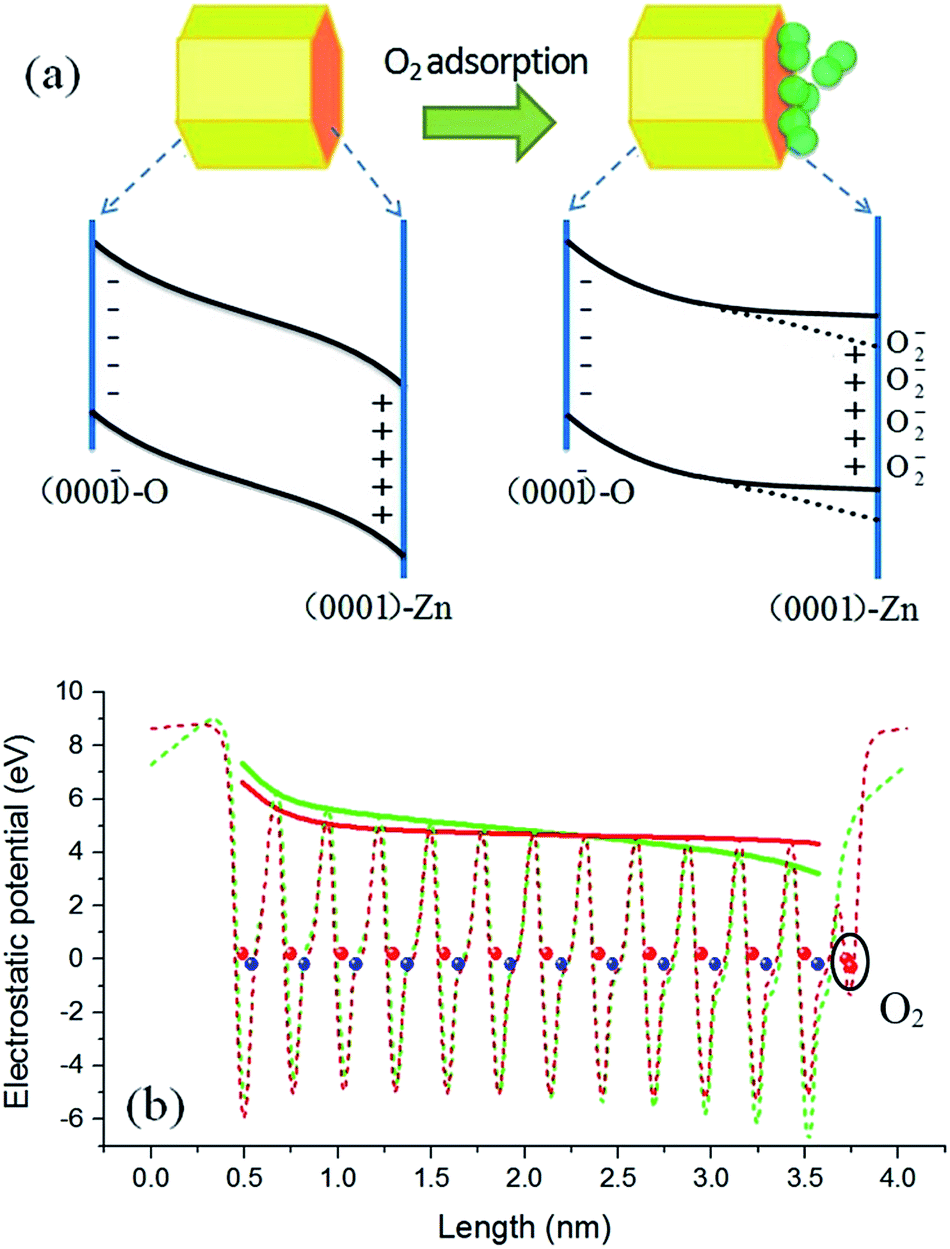 | ||
| Fig. 5 Proposed schematic diagram (a) and theoretical calculations (b) of the band bending in ZnO QDs before and after O2 adsorption. The red and blue balls in (b) flag the positions of the O and Zn atomic layers. | ||
In addition to the polar surface charge effect, we further propose that the O2 molecules prefer to adsorb on the Zn-terminated (0001) surfaces of the QDs. This is because there are unpaired electrons in the dangling bonds of the surfaces and they locate at relatively higher energy states. O2 adsorption can shift these electrons to the lower energy states (the lowest unoccupied molecular orbital of O2). As argued earlier, the adsorbed O2 molecules tend to induce upward band bending, being just the opposite to that induced by the clean (0001) surface. Therefore, adsorption of O2 molecules may bring out a compensation effect, weakening or even eliminating the original band bending in the Zn-terminated side. A schematic diagram of this mechanism is shown in the right part of Fig. 5(a). The radiative recombination probability of electron–hole pairs is thus improved under the circumstance of O2 adsorption, and the emission intensity is enhanced. Because the PL intensity in pure oxygen condition is stronger than that in air (see Fig. 4), we deduce that in normal air conditions the band bending in the Zn-terminated side is just weakened, not fully eliminated; in other words, as the dotted lines but not the solid lines in Fig. 5(a). For NWs, O2 molecules have no choice to adsorb on the nonpolar surface and thus no compensation effect occurs, leading to upward band bending and weak luminescence intensity.
To get further support for the proposed model, density functional theory based calculations were performed to simulate the surface induced band bending. The local density approximation plus U method implemented in the VASP code and the projector augmented-wave potential were adopted.39–41 A slab model including twelve ZnO bilayers was used to describe the polar surfaces, corresponding to a ZnO QD with diameter of about 3.2 nm. The calculation results are shown in Fig. 5(b), in which the dashed curves are the plane-averaged electrostatic potential distribution along the c-axis orientation before (green) and after (red) O2 adsorption, and the envelope curve (solid lines) can be identified as the relative position of the band edge. The red curve represents a result with the O2 adsorption coverage of a 0.5 monolayer, which is the best coverage for compensating the polar surface charging effect.42,43 It can be seen that under such circumstances the original band bending is significantly flattened, which is very consistent with the speculation. A dead-layer model was widely used to quantitatively evaluate the PL intensity variation with the depth of depletion layer.38,44 In this model the dead layer is roughly equivalent to the depletion region and in this region the radiative recombination of electron–hole pairs was thought to be fully depressed. Therefore, there is little PL intensity coming from the depletion region (dead layer). The PL intensity (IPL) is determined by IPL ∝ I0![[thin space (1/6-em)]](https://www.rsc.org/images/entities/char_2009.gif) exp(−αD), where I0 is the incident light intensity, α is the absorption coefficient, and D is the length of the depletion region. For the ZnO QDs without O2 adsorption, the depletion region covers the whole dot, as shown by the solid green curve in Fig. 5(b). This time the luminescence should be fully quenched according to the dead-layer model. This is just the experimental result shown in Fig. 2(a) where the PL intensity is very weak at high vacuum conditions. As shown by the solid red curve in Fig. 5(b), the band was flattened in length by about 85% after O2 adsorption. This means that about an 85% volume of the sample changes from nonradiative to radiative with O2 adsorption. Consequently, the PL intensity change of the same magnitude should be compatible and convincing.
exp(−αD), where I0 is the incident light intensity, α is the absorption coefficient, and D is the length of the depletion region. For the ZnO QDs without O2 adsorption, the depletion region covers the whole dot, as shown by the solid green curve in Fig. 5(b). This time the luminescence should be fully quenched according to the dead-layer model. This is just the experimental result shown in Fig. 2(a) where the PL intensity is very weak at high vacuum conditions. As shown by the solid red curve in Fig. 5(b), the band was flattened in length by about 85% after O2 adsorption. This means that about an 85% volume of the sample changes from nonradiative to radiative with O2 adsorption. Consequently, the PL intensity change of the same magnitude should be compatible and convincing.
In summary, the visible PL intensity of ZnO QDs shows a high sensitivity to the partial pressure of oxygen. When the partial gas pressure is decreased, the visible emission decreases significantly. This phenomenon is just the opposite to that of ZnO NWs. By taking into consideration the compensation effect between the polar surface charging and O2 adsorption induced band bending, a physical model is proposed to illustrate the abnormal phenomenon. The model is also strongly supported by the density functional theoretical calculations, which emphasizes that QDs of a wurtzite semiconductor may not be supposed as isotropic spheres. The polar surfaces may have a significant influence on its optical properties.
Acknowledgements
The authors gratefully acknowledge the financial support of China National Natural Science Funds (No. 11204231, 21373156), the National Key R&D Program of China (2016YFB1102500) and the Fundamental Research Funds for the Central Universities.References
- C. F. Klingshirn, A. Waag, A. Hoffmann and J. Geurts, Zinc Oxide: From Fundamental Properties Towards Novel Applications, Springer Science & Business Media, 2010 Search PubMed.
- L. Schmidt-Mende and J. L. MacManus-Driscoll, Mater. Today, 2007, 10, 40–48 CrossRef CAS.
- I. S. ADong, B. W. Kwon and H. P. Dong, Nat. Nanotechnol., 2012, 7, 465–471 CrossRef PubMed.
- Ü. Özgür, Y. I. Alivov, C. Liu, A. Teke, M. A. Reshchikov, S. Doğan, V. Avrutin, S.-J. Cho and H. Morkoç, J. Appl. Phys., 2005, 98, 41301 CrossRef.
- M. H. Huang, S. Mao, H. Feick, H. Yan, Y. Wu, H. Kind, E. Weber, R. Russo and P. Yang, Science, 2001, 292, 1897–1899 CrossRef CAS PubMed.
- Y. Q. Su, Y. Zhu, D. Yong, M. Chen, L. Su, A. Chen, Y. Wu, B. Pan and Z. Tang, J. Phys. Chem. Lett., 2016, 7, 1484–1489 CrossRef CAS PubMed.
- H. Ye, G. Chen, H. Niu, Y. Zhu, L. Shao and Z. Qiao, J. Phys. Chem. C, 2013, 117, 15976–15983 CAS.
- K. Yadav, S. K. Gahlaut, B. R. Mehta and J. P. Singh, Appl. Phys. Lett., 2016, 108, 71602 CrossRef.
- F. Fan, Y. Feng and S. Bai, Sens. Actuators, B, 2013, 185, 377–382 CrossRef CAS.
- Q. Huang, D. Zeng and H. Li, Nanoscale, 2012, 4, 5651–5658 RSC.
- K. Matsuyama, N. Ihsan, K. Irie, K. Mishima, T. Okuyama and H. Muto, J. Colloid Interface Sci., 2013, 399, 19–25 CrossRef CAS PubMed.
- S. Mahamuni, K. Borgohain, B. S. Bendre, V. J. Leppert and S. H. Risbud, J. Appl. Phys., 1999, 85, 2861–2865 CrossRef CAS.
- H. Zhou, H. Alves and D. M. Hofmann, Appl. Phys. Lett., 2002, 80, 210–212 CrossRef CAS.
- K. A. Alim, V. A. Fonoberov and A. A. Balandin, Appl. Phys. Lett., 2005, 86, 53103–531033 CrossRef.
- K.-F. Lin, H.-M. Cheng, H.-C. Hsu, L.-J. Lin and W.-F. Hsieh, Chem. Phys. Lett., 2005, 409, 208–211 CrossRef CAS.
- X. Xu, C. Xu, X. Wang, Y. Lin, J. Dai and J. Hu, CrystEngComm, 2013, 15, 977 RSC.
- J. Q. Ning, C. C. Zheng, X. H. Zhang and S. J. Xu, Nanoscale, 2015, 7, 17482–17487 RSC.
- L. Zhang, L. Yin and C. Wang, J. Phys. Chem. C, 2010, 114, 9651–9658 CAS.
- J. H. Jia, B. Y. Yi and Q. L. Zhou, Phys. Chem. Chem. Phys., 2014, 16, 5480–5484 RSC.
- Y. Zhang, H. Wang, H. Jiang and X. Wang, Nanoscale, 2012, 4, 3530–3535 RSC.
- S. Li, Z. Sun, R. Li, M. Dong, L. Zhang, W. Qi, X. Zhang and H. Wang, Sci. Rep., 2015, 5, 8475 CrossRef CAS PubMed.
- S. Bai, J. Hu and D. Li, J. Mater. Chem., 2011, 21, 12288–12294 RSC.
- Y. S. Lee, D. J. Lee and Y. K. Seo, Phys. Semicond. Int. Conf. Phys. Semicond., 2011, vol. 1399, pp. 525–526 Search PubMed.
- M. Ghosh, R. S. Ningthoujam, R. K. Vatsa, D. Das, V. Nataraju, S. C. Gadkari, S. K. Gupta and D. Bahadur, J. Appl. Phys., 2011, 110, 54309 CrossRef.
- Y. Lin, D. Wang, Q. Zhao, Z. Li, Y. Ma and M. Yang, Nanotechnology, 2006, 17, 2110–2115 CrossRef CAS.
- Y. Li, M. Liu, T. Lv, Q. Wang, Y. Zou, X. Lian and H. Liu, Electron. Mater. Lett., 2015, 11, 1085–1092 CrossRef CAS.
- A. Stevanovic, M. Büttner, Z. Zhang and J. T. Yates, J. Am. Chem. Soc., 2012, 134, 324–332 CrossRef CAS PubMed.
- M. Ghosh and A. K. Raychaudhuri, Appl. Phys. Lett., 2011, 98, 153109 CrossRef.
- A. R. Gheisi, C. Neygandhi, A. K. Sternig, E. Carrasco, H. Marbach, D. Thomele and O. Diwald, Phys. Chem. Chem. Phys., 2014, 16, 23922–23929 RSC.
- L. Spanhel and M. A. Anderson, J. Am. Chem. Soc., 1991, 113, 2826–2833 CrossRef CAS.
- X. Duan, G. Chen, C. Li, Y. Yin, W. Jin, L. Guo, H. Ye, Y. Zhu and Y. Wu, Nanotechnology, 2016, 27, 295601 CrossRef PubMed.
- L. Ding, B. K. Li, H. T. He, W. K. Ge, J. N. Wang, J. Q. Ning, X. M. Dai, C. C. Ling and S. J. Xu, J. Appl. Phys., 2009, 105, 53511 CrossRef.
- S. J. Xu, S.-J. Xiong and S. L. Shi, J. Chem. Phys., 2005, 123, 221105 CrossRef CAS PubMed.
- H. Ye, Z. Su, F. Tang, M. Wang, G. Chen, J. Wang and S. Xu, Sci. Rep., 2017, 7, 41460 CrossRef CAS PubMed.
- Y. H. Leung, X. Y. Chen, A. M. C. Ng, M. Y. Guo, F. Z. Liu, A. B. Djurišić, W. K. Chan, X. Q. Shi and M. A. Van Hove, Appl. Surf. Sci., 2013, 271, 202–209 CrossRef CAS.
- X. Xu, C. Xu, Z. Shi, C. Yang, B. Yu and J. Hu, J. Appl. Phys., 2012, 111, 83521 CrossRef.
- D. Li, Y. H. Leung, A. B. Djurišić, Z. T. Liu, M. H. Xie, S. L. Shi, S. J. Xu and W. K. Chan, Appl. Phys. Lett., 2004, 85, 1601–1603 CrossRef CAS.
- Z. Zhang and J. T. Yates, Chem. Rev., 2012, 112, 5520–5551 CrossRef CAS PubMed.
- G. Kresse and D. Joubert, Phys. Rev. B: Condens. Matter Mater. Phys., 1999, 59, 1758–1775 CrossRef CAS.
- G. Makov and M. Payne, Phys. Rev. B: Condens. Matter Mater. Phys., 1995, 51, 4014–4022 CrossRef CAS.
- M. Gajdoš, K. Hummer, G. Kresse, J. Furthmüller and F. Bechstedt, Phys. Rev. B: Condens. Matter Mater. Phys., 2006, 73, 045112 CrossRef.
- H. Ye, G. Chen, Y. Zhu and S.-H. Wei, Phys. Rev. B: Condens. Matter Mater. Phys., 2008, 77, 033302 CrossRef.
- H. Ye, G. Chen, H. Niu, Y. Zhu, L. Shao and Z. Qiao, J. Phys. Chem. C, 2013, 117, 15976–15983 CAS.
- R. E. Hollingsworth and J. R. Sites, J. Appl. Phys., 1982, 53, 5357–5358 CrossRef CAS.
| This journal is © The Royal Society of Chemistry 2017 |