
 Open Access Article
 This Open Access Article is licensed under a
 Creative Commons Attribution 3.0 Unported Licence
“Close network” effect of a ZnO micro/nanoporous array allows high UV-irradiated NO2 sensing performance†
Xingsong Suab,
Lei Gaoa,
Fei Zhoua,
Weiping Caia and
Guotao Duan *a
*a
aKey Lab of Materials Physics, Anhui Key Lab of Nanomaterials and Nanotechnology, Institute of Solid State Physics, Chinese Academy of Sciences, Hefei, 230031, PR China. E-mail: duangt@issp.ac.cn
bUniversity of Science and Technology of China, Hefei, 230026, PR China
First published on 12th April 2017
Abstract
ZnO micro/nanoporous arrays with controlled morphologies were fabricated by a monolayer colloidal crystal and solution-dipping strategy. Then their UV-irradiated NO2 sensing performances, especially the morpholgy-correlated effects were studied in detail. It was found that a close-network micro/nanoporous array film (CNPAF) and bowl-like micro/nanoporous array film (BLPAF), which were prepared with different concentrations of precursors, presented different sensing performances. The former showed higher sensitivity, lower detecting limit, and shorter response/recovery times. The “close network” effect was proposed to explain the mechanism behind these results. First, CNPAF has a closed network structure, which would decrease the resistance of the film and provide more sensing spots for NO2, which enhanced sensitivity. Second, according to the hydrokinetics of microluidic flow, the closed network structure may localize the flowing gas, which led to shorter response and recovery times of the sensor. This work clarified the morphology-correlated effect of ZnO micro/nanoporous arrays on their NO2 sensing performances, and it would be helpful for the realization of room temperature NO2 sensors.
Introduction
Nitrogen dioxide (NO2) is a combustion-supporting material and main atmospheric pollutant that causes acid rain and even explosion.1,2 So it is urgently needed to detect or monitor ppb-level NO2 in the field of detecting explosions with high performance NO2 sensors.3,4 Semiconductor gas sensors are becoming more and more attractive in NO2 detection in recent years because of their high sensitivity, long-term stability and quicker response and recovery times.5–8 However, for the traditional semiconductor gas sensors, they are generally operated at a high temperature (175–400 °C).9,10 The high operation temperature limits the applications of gas sensors in many areas. Such high operating temperatures may induce ignition of flammable and explosive gases, and also cause high power consumption of the sensors.To solve the above problems, a few room temperature NO2 sensors have been designed and manufactured by using new sensitive materials11,12 and new techniques, such a micro-electro mechanical system (MEMS) fabrication,13 doping of novel metals14,15 and ultraviolet (UV) irradiation etc.16,17 In these techniques, UV irradiation has attracted increasing attention as a promising strategy. It has been reported that a large number of photo-generated carriers diffuse to the surface of semiconductor under UV irradiation. Then the charge carries are involved in the reaction with electron donors or acceptors readily, which induces the change of photocurrent intensity.18–20 Based on the above theory, many researchers have found that UV irradiation can improve the sensing performance of semiconducting gas sensors.
Zinc oxide (ZnO), with a wide band gap of 3.37 eV, has been considered as one of the promising materials in the field of gas sensors operated under UV light irradiation.21–24 The sensing performances and optical properties of ZnO based devices are influenced significantly by its surface morphologies. So many researches were focused on the formation of various morphology of ZnO thin film with one step physical deposition routes, such as vacuum evaporation and sputtering methods.25–28 Alternatively, ZnO film can also be deposited by spin- or dip-coating method using ZnO slurry.29–31 However, these techniques usually show some drawbacks. For instance, the one step physical deposition routes usually have the acknowledged disadvantages of high cost, while ZnO thin films obtained by the spin- or dip-coating techniques are mostly limited to flat substrates, difficult to maintain uniform on a large scale. The presence of irregular interstitial areas and inhomogeneous aggregations leads to poor repeatability and uncertain performance of the finally ZnO devices. In recent years, colloidal lithography by using polystyrene sphere (PS) monolayer colloidal crystal (MCC) have been proven an effective method to synthesize micro/nanostructured arrays film with nice homogeneity. Thus it can also be used as strategy to formation gas-sensing film sensors.32–34
In this work, ZnO micro/nanostructured arrays films of different morphologies were fabricated based on PS MCC, and their sensing properties under UV irradiation were also studied. It has been found that the sensing performances are strongly morphology-dependence: ZnO CNPAF sensors show higher sensitivity, lower detecting limit and shorter response/recovery time compared to ZnO BLPAF sensor. Then a “close network” effect is further proposed to explain the behind mechanism. This work clarified the morphology-correlated effect of ZnO micro/nanoporous arrays on their NO2 sensing performances, which is very important for the realization of NO2 room temperature sensors. The results and discussion are detailed in the following sections.
Experimental section
Fabrication of ZnO micro/nanoporous porous films
The fabrication of PS (500 nm) monolayer colloidal crystal (PS MCC) follows our previous report with a minor modification.35–38 The freshly fabricated PS MCC on the glass slides possesses the feature of transferability. The transfer process from the glass slide to a silicon wafer (20 mm × 20 mm), glass slide (50 mm) or a flat ceramic electrode (2.5 mm × 2.0 mm) substrate is illustrated in Fig. 1c, d and S1 (see ESI†). The transferred PS MCC on the flat substrate was firstly surface-modified by irradiation in the ultraviolet ozone cleaner for 5 min to improve its mechanical flexibility and surface hydrophilicity. Then 0.1 mol L−1 and 0.2 mol L−1 Zn(AC)2·2H2O were taken as precursor solutions. When immersed into the precursor solution, the PS MCC template was separated from the glass slide and integrally floated on the surface of the precursor, as shown in Fig. 1c. Then, a flat substrate was used to pick up the template carefully, as shown in Fig. 1d. The samples were dried at 80 °C for an hours. The final annealing was carried out at 450 °C for 2 h to remove the PSs in air, leaving a bowl-like or close-network micro/nanoporous porous films on the substrate, forming ZnO due to the decomposition of Zn(AC)2·2H2O. The heating rate and cooling rate were about 2 °C min−1.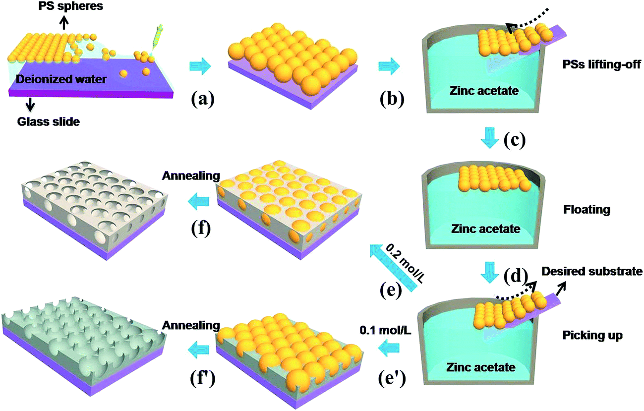 | ||
| Fig. 1 Schematic illustration of fabrication routes: the processing steps used to in situ fabricate ZnO ordered porous an Al2O3 flat ceramic electrodes. (b) The colloidal template is stripped off and (c) floated on the surface of precursor solution; (d) the floating monolayer colloidal template is picked up by the Al2O3 flat ceramic electrodes; (e) and (e′) the Al2O3 flat ceramic electrodes covered with monolayer colloidal template is dried in the dying oven; (f) and (f′) the ZnO micro/nanoporous array-film is formed after annealing at a high temperature (450 °C). | ||
Characterization and gas sensing measurements
The microstructures and morphologies of the as-prepared samples were characterized by using field-emission scanning electron microscopy (FEEM, Srion200). Phase formation of the films were carried out on a Philips X'pert powder X-ray diffractometer using CuKα radiation (0.15419 nm). Gas sensing properties were measured for the ZnO porous films covered on Al2O3 flat ceramic substrate using a static test system which includes a test chamber and a multimeter/DC power supply (Agilent mod. U3606A and U8002A). The photoelectric gas sensing measurement was carried out under irradiation of monochromatic light (365 nm) (CEL-LED 100-365, Aulight). The UV light was adjusted to 5 W and the distance between the UV lamp and the thin film sample was 15 cm. The light beam was 8 cm in diameter and vertically irradiated on the sensing film through a quartz window on the test chamber. The UV light was turned on after the film was put into the test chamber. After a steady resistance was measured for the film, a certain amount of NO2 was injected into the test chamber and the response was measured. The NO2 concentration in the chamber was calculated according to the injected amount. After the irradiation for ∼1000 s, the UV light was turned off. All measurements were operated at room temperature (25 °C).Results and discussion
The samples were fabricated by taking transferred PS monolayer colloidal crystal (MCC) template and sequent heat treatment, as is shown in Fig. 1. Fig. 2 shows the XRD pattern of the as-prepared samples. All diffraction peaks can be indexed to a wurtzite structure of the ZnO material (JCPDF card no. 00-036-1451), no characteristic peaks from other crystalline forms are detected in the XRD pattern. | ||
| Fig. 2 XRD pattern of ZnO micro/nanoporous ordered arrays: (a) 0.1 mol L−1; (b) 0.2 mol L−1. | ||
Fig. 3 shows the SEM images of ZnO micro/nanoporous ordered arrays (on a silicon wafer substrate), with different precursor concentrations, dried in an oven at 80 °C for an hours, and then heated at 450 °C for two hours. A series of porous ordered arrays with different morphologies was obtained. When the precursor concentration is 0.1 M or 0.2 M, the micro/nanoporous array films with uniform pore size was formed on the flat substrates, as shown in Fig. 3A and C. The micro/nanoporous array films with two different morphologies were more clearly revealed by tilted views, as illustrated in Fig. 3B and D. A low concentration (0.1 M) gives rise to pores with nearly circular upper-end openings, which is called bowl-like structure (Fig. 3B). As the precursor concentration increases to 0.2 M, it is found that some small holes at the interstitial position of the closely packed PSs and nanogaps on pore walls (skeletons) appear. The micro/nanoporous arrays film is actually a nearly spherical hollow array with truncated tops as openings, which is named as close-network structure (Fig. 3D). The thickness of the CNPAF and BLPAF are 400 nm and 280 nm, respectively (Fig. S2†). The truncated hollow sphere arrays with these close networks structure are a key factor to enhance sensing performances compared to the micro/nanoporous arrays film of bowl-like. We can also fabricate a larger area of micro/nanostructure porous ordered array film (Fig. S3 see ESI†).
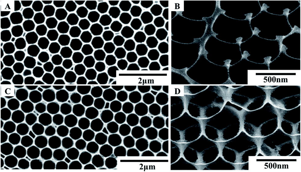 | ||
| Fig. 3 SEM images of ZnO micro/nanoporous arrays obtained from 500 nm PS film templates at different precursor content of zinc acetate (Zn(AC)2·2H2O): (A and B): 0.1 mol L−1; (C and D): 0.2 mol L−1. (B) and (D) are oblique views. | ||
The gas sensing properties of the ZnO micro/nanoporous arrays films for NO2 were measured under UV light irradiation at room temperature. The gas response of sensors is defined as (Rgas/Rair), where Rair is the resistance in air and Rgas is the resistance in the presence of NO2 under UV light irradiation (0.35 mW cm−2). The sensitivity increased instantaneously to a maximum sensitivity, which was maintained at the maximum sensitivity upon exposure to NO2 and recovered completely to the initial value upon the removal of NO2. The gas response curves of sensors to different concentrations for NO2 are shown in Fig. 4. It can be seen that the gas response transients exhibited stable and reproducible response and recovery characteristics, and the response increase obviously for two samples with the increasing NO2 concentrations. Fig. 5A presents the response of BLPAFs and CNPAFs as a function of the NO2 concentration. It is obvious that the sensor of CNPAFs exhibits a stronger response to NO2 measured at room temperature under UV light irradiation than the sensor based on BLPAF. For example, the responses of bowl-like ZnO micro/nanoporous array sensor and close-network ZnO micro/nanoporous array sensor to 50 ppm of NO2 were 4.5 and 27.5, respectively. The CNPAF based sensor also exhibited a faster response (Fig. 5B) and recovery time (Fig. 5C) than BLPAF sensor at the same NO2 concentration. For example, the response time of the sensor based on BLPAF to 50 ppm was 125 s, while the response time of the sensor based on CNPAF was 35 s. The recovery time of sensor based on CNPAF to 50 ppm was shortened from 210 s to 65 s corresponding to that of BLPAF based sensor. Herein, the response and recovery times of the sensors are defined as the times to reach 90% of resistance change upon exposure to NO2 and air, respectively. In addition, the gas sensing properties of the CNPAF and BLPAF have good repeatability, as shown in Fig. S4.†
 | ||
| Fig. 4 Gas response transients of close-network ZnO micro/nanoporous array films (A) and bowl-like ZnO micro/nanoporous array films (B) toward NO2 gas at room temperature under UV light irradiation. | ||
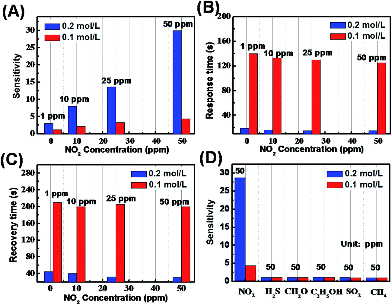 | ||
| Fig. 5 (A) Response, (B) response time, (C) recovery time of the bowl-like ZnO micro/nanoporous array films and close-network ZnO micro/nanoporous array films toward NO2 gas at room temperature under UV light irradiation. (D) Comparison of response of ZnO micro/nanoporous array gas sensor to different kinds of flammable gases at room temperature under UV light irradiation. | ||
Besides NO2, the sensing performances of the two micro/nanoporous arrays sensors to other gases including H2S, CH2O, C2H5OH, SO2 and CH4 at room temperature were investigated under UV light irradiation, as shown in Fig. 5D. Both the bowl-like and close-network ZnO micro/nanoporous arrays film sensors exhibited a stronger response to NO2 than to other gases. The sensor of CNPAFs showed lower normalized response to the other gases than the BLPAF based sensor, suggesting that the close-network sensor has superior selectivity for NO2 gas compared to the bowl-like sensor. The selectivity of the sensor is influenced by various factors. For the study, the structures and bond dissociation energies of gas molecules are significant influences. The NO2 band is 221 kJ mol−1, which is smaller than other gases at room temperature. Therefore, the bond dissociation energies of NO2 are easily broken to participate in the reaction with the sensing material in the process of chemical adsorption. In addition, other gases because of their high bonding energy would be reluctant to react at room temperature, but display lower response. So the operating temperature is also an important factor. The operating temperature depends on the orbital energy of gas molecule, adsorption mode and amount of gas and so on33,34 Therefore, the selectivity may be distinct different operating temperatures. In a word, the high selectivity makes the ZnO micro/nanostructure ordered porous array films to be a remarkable sensing material in fabrication of NO2 sensor.
A low determination limit is important for the gas sensors in trace or ultratrace target gas analysis, especially in practical application. To observe the sensor response to 100 ppb NO2 in ambient gas which even contains low-concentration NO2, the continuous tests without recoveries were taken in the concentration range from 100 ppb to 1000 ppb at room temperature under UV light irradiation, as shown in Fig. 6. It is obvious that the CNPAF based sensor can determine NO2 gas as low as 100 ppb, while it cannot be detected at such a low concentration by the BLPAF based sensor.
 | ||
| Fig. 6 Continuous test without recoveries to 100–1000 ppb NO2 concentration range at room temperature under UV light irradiation. | ||
When the sensors are exposed to air at room temperature without UV irradiation, the adsorbed oxygen molecules on the surface of zinc oxide are in a dynamic equilibrium state. The possible model for enhanced sensing performance of the two sensors is shown in Fig. 7. Electrons are transferred from the conduction band to the adsorbed oxygen atoms, and forming ionic species, such as O−, O2− and O2− (Fig. 7a and a′). Of these oxygen species, O2− is dominant at room temperature.38–41 When the ZnO films are irradiated with UV light (365 nm) of energy higher than the band gap (3.22 eV), as shown in Fig. S5.† The electrons in the valence band are excited to the conduction band, and holes are generated in valence band. The surface of ZnO porous films will generate a large number of photon-generated electrons and holes, and excited electrons move the valence band. On their way to the ZnO micro/nanoporous film surface, some photon-generated electrons and holes will recombine with each other and many photon-generated holes react with negatively charged adsorbed oxygen ions on the surface of ZnO porous films. The result of these reactions is that the width of the surface depletion layer in the skeleton of ZnO porous films is reduced (Fig. 7b and b′). Oxygen species were photodesorpted from the surface.42 Upon exposure to NO2 gas, the NO2 gas adsorbs on the sensors and the remaining photo-generated electrons were released from the material surface, and were attracted to the adsorbed NO2 molecules because an oxidizing gas, such as NO2, acts as an electron acceptor (Fig. 7c and c′), as shown in the following reaction:34,41
| 2NO2 (g) + e− (hν) → 2NO (hν) + O2− (hν) |
 | ||
| Fig. 7 Schematic of (A) ZnO close-network and (B) ZnO bowl-like porous array surface reactions under different conditions: (a) and (a′) in the dark; (b) and (b′) with UV light irradiation; (c) and (c′) in NO2 gas with UV light irradiation. | ||
This reaction further broadens the width of the surface depletion layer, which led to increase of the sensors resistance.
To investigate the relationship between crystal morphologies and sensing property, previous publication of the ZnO sensing work have been tabulated, as shown in Table S1.† It is found that the gas properties of sensitive materials with different morphologies are significantly different, such as the response of the needle-like ZnO nanorods is 184.5, while the response of flower-like ZnO nanorods is 44.8. The high response of sensing materials to target gas is due to their high surface-to-volume ratio, which results in more O− ions adsorption on the material surface. Thus, the possible reaction between the target gas and the O− ions increased and resulted to the increase of the conduction, which also indicates that the equilibrium density of chemisorbed O− ions was maximal at the optimum operating temperature. However, the influence of sensitive materials with different morphology to the gas sensing properties are complicated, it not only has to consider the surface-to-volume ratio, but also crystallographic orientation of crystalline planes and surface architecture.43,44 Therefore, the enhanced sensing performance of the CNPAF sensor relative to that of the BLPAF sensor can be explained by a combination of electronic and chemical mechanisms. A critical difference between the CNPAF and BLPAF sensors is the presence of close-network on the top of bowl-like structure sensors, as shown in Fig. 8. It is well know that the gas chemical reactions occur on the surface of nanostructure films. So the close-network structure of ZnO porous film should be considered to explain the enhanced sensing performance of the CNPAF sensor. It is worth noting that the gas-sensing response increased gradually with increase of specific surface area, which indicates that the large specific area will be well helpful for the gas detection.27,45 In this paper, the CNPAF with close-network structure is primary explanation for enhanced sensing performance of the CNPAF sensor. On the one hand, it is well known that the reactions of the ZnO micro/nanoporous array sensors and the gas molecules takes place on the backbone of the micro/nanoporous array film. The primary cell surface areas of CNPAF and BLPAF were 0.494 and 0.303 μm2 by theoretical calculation (Fig. 8C and D), respectively. It is shown that the sensitive activation sites numbers of the CNPAF are more than that of the BLPAF in the reactions with the NO2 gases. Correspondingly, the number of oxygen ions chemisorbing will be increased, resulting in the increase of the gas response for CNPAF sensor. On the other hand, one of the fundamental principles used in the analysis of response and recovery time is known as the hydrokinetic of microluidic flow. There is a small triangular hole at the interstitial position of the closely packed truncated hollow sphere, which may be produce “draught effect”. It is a key factor that may promote the localized gas flowing, which thus lead to short response and recovery times of the sensor. This part of the experiment needs to be further confirmed.
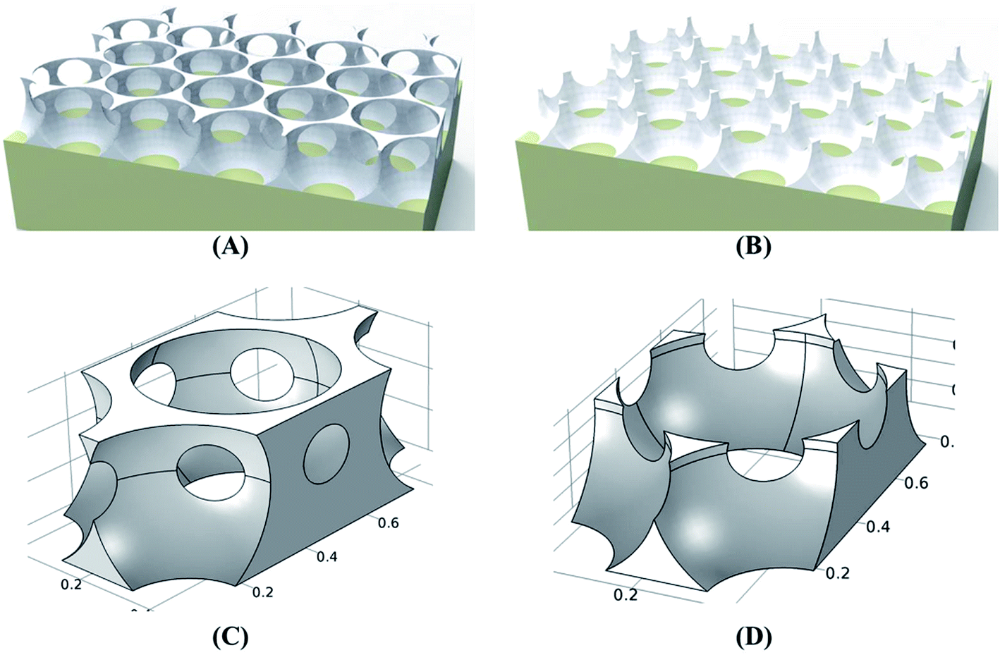 | ||
| Fig. 8 Schematic view of ZnO micro/nanoporous porous film (A) CNPAF; (B) BLPAF. (C) and (D) Represent the unit cell of (A) and (B), respectively. | ||
Conclusion
In summary, the sensors based on CNPAF and BLPAF were prepared by transferring a solution-dipped self-organized colloidal template onto the flat ceramic electrode with different concentration of precursor solution and sequent heat treatment. Their sensing properties to NO2 are studied in detail. Interestingly, compared with BLPAF-based sensors, the sensors of CNPAF exhibits shorter recovery and response times, higher sensitivity and better selectivity to NO2 gas against other interfering gases. These enhanced sensing properties may be due to produce “draught effect”, and provide more sensitive activation sites numbers of CNPAF to NO2. This work clarified the morphology-correlated effect of ZnO micro/nanoporous arrays on their NO2 sensing performances, and it would be helpful for the realization of NO2 room temperature sensors.Acknowledgements
The authors acknowledge the financial supports from National Key Research and Development Plan (2016YFC0201103), the financial supports from Natural Science Foundation of China (Grant No. 11674320 and 51471161), Anhui Provincial Natural Science Foundation for Distinguished Young Scholar (1408085J10), Youth Innovation Promotion Association CAS, and Key Research Projects of the Frontier Science CAS (QYZDB-SSW-JSC017).References
- C. Baratto, G. Sberveglieri, A. Onischuk, B. Caruso and S. D. Stasio, Sens. Actuators, B, 2004, 100, 261 CrossRef CAS.
- L. Chen and S. C. Tsang, Sens. Actuators, B, 2003, 89, 68 CrossRef CAS.
- J. S. Kima, J. W. Yoon, Y. J. Hong, Y. C. Kang, F. A. Hady, A. A. Wazzan and J. H. Lee, Sens. Actuators, B, 2016, 229, 561 CrossRef.
- Y. X. Li, B. Y. Zu, Y. N. Guo, K. Li, H. B. Zeng and X. C. Dou, Small, 2016, 12, 1420 CrossRef CAS PubMed.
- S. H. Park, S. Y. An, Y. G. Mun and C. M. Lee, Curr. Appl. Phys., 2014, 14, 57 CrossRef.
- Y. X. Qin, X. J. Zhang, Y. Liu and W. W. Xie, J. Alloys Compd., 2016, 673, 364 CrossRef CAS.
- T. Hyodo, K. Sasahara, Y. Shimizu and M. Egashira, Sens. Actuators, B, 2005, 106, 580–590 CrossRef CAS.
- C. J. Chang, C. K. Liu, C. C. Chen, C. Y. Chen and E. H. Kuo, Thin Solid Films, 2011, 520, 1546–1553 CrossRef CAS.
- T. Hamaguchi, N. Yabuki, M. Uno, S. Yamanaka, M. Egashira, Y. Shimizu and T. Hyodo, Sens. Actuators, B, 2006, 113, 852–856 CrossRef CAS.
- C. J. Chang, C. Y. Liu, J. K. Chen and M. H. Hsu, Ceram. Int., 2014, 40, 10867–10875 CrossRef CAS.
- K. Dunst, D. Jurków and P. Jasiński, Sens. Actuators, B, 2016, 229, 155 CrossRef CAS.
- V. Blechta, M. M. Karolin, V. V. Drogowska and M. Kalbá, Sens. Actuators, B, 2016, 226, 299 CrossRef CAS.
- J. H. Yoon and J. S. Kim, Solid State Ionics, 2011, 192, 668 CrossRef CAS.
- Y. L. Wang, X. B. Cui, Q. Y. Yang, J. Liu, Y. Gao, P. Sun and G. Y. Lu, Sens. Actuators, B, 2016, 225, 544 CrossRef CAS.
- P. V. Adhyapak, S. P. Meshram, A. A. Pawar, D. P. Amalnerkar, U. P. Mulik and I. S. Mulla, Ceram. Int., 2014, 40, 12105 CrossRef CAS.
- T. Wagner, C. D. Kohl, C. Malagù, N. Donato, M. Latino, G. Neri and M. Tiemann, Sens. Actuators, B, 2013, 187, 488 CrossRef CAS.
- E. Comini, G. Faglia and G. Sberveglieri, Sens. Actuators, B, 2001, 78, 73 CrossRef CAS.
- S. J. Pearton, F. Ren, Y. L. Wang, B. H. Chu, K. H. Chen, C. Y. Chang, W. Lim, J. S. Lin and D. P. Norton, Prog. Mater. Sci., 2010, 55, 1 CrossRef.
- S. Mishra, C. Ghanshyam, N. Ram, R. P. Bajpai and R. K. Bedi, Sens. Actuators, B, 2004, 97, 387 CrossRef CAS.
- L. Peng, Q. D. Zhao, D. J. Wang, J. L. Zhai, P. Wang, S. Pang and T. F. Xie, Sens. Actuators, B, 2009, 136, 80 CrossRef CAS.
- D. An, Y. Li, X. X. Lian, Y. L. Zou and G. Z. Deng, Colloids Surf., A, 2014, 447, 81 CrossRef CAS.
- P. Afzali, Y. Abdi and E. Arzi, Sens. Actuators, B, 2014, 195, 92 CrossRef CAS.
- S. G. Park, G. J. Sun, C. Y. Jin, H. W. Kim, S. M. Lee and C. M. Lee, ACS Appl. Mater. Interfaces, 2016, 8, 2805 CAS.
- L. N. Han, D. J. Wang, J. B. Cui, L. P. Chen, T. F. Jiang and Y. H. Lin, J. Mater. Chem., 2012, 22, 12915 RSC.
- L. Luo, B. D. Sosnowchik and L. W. Lin, Nanotechnology, 2010, 21, 495 CrossRef PubMed.
- Y. X. Cai, X. W. Li, P. Sun, B. Wang, F. G. Liu, P. F. Cheng, S. S. Du and G. Y. Lu, Mater. Lett., 2013, 112, 36 CrossRef CAS.
- S. H. Park, H. S. Ko, S. M. Lee, H. W. Kim and C. M. Lee, Thin Solid Films, 2014, 570, 298 CrossRef CAS.
- K. Kourosh, V. Aravind, H. Moon, H. Zheng, B. Michael and M. S. Strano, Chem. Mater., 2010, 19, 5660 Search PubMed.
- J. B. Cui, L. Q. Shi, T. F. Xie, D. J. Wang and Y. H. Lin, Sens. Actuators, B, 2016, 227, 220 CrossRef CAS.
- J. L. Zhai, L. L. Wang, D. J. Wang, Y. H. Lin, D. Q. He and T. F. Xie, Sens. Actuators, B, 2012, 161, 292 CrossRef CAS.
- J. Gong, Y. H. Li, X. S. Chai, Z. S. Hu and Y. L. Deng, J. Phys. Chem. C, 2010, 114, 1293 CAS.
- G. T. Duan, W. P. Cai, Y. Li, B. Q. Cao and Y. Y. Luo, J. Phys. Chem. B, 2006, 14, 7184 CrossRef PubMed.
- Y. X. Li, N. Chen, D. Y. Deng, X. X. Xing, X. C. Xiao and Y. D. Wang, Sens. Actuators, B, 2017, 238, 264 CrossRef CAS.
- H. Y. Du, J. Wang, P. Yu, N. S. Yu, Y. H. Sun and J. L. Tian, J. Nanopart. Res., 2014, 16, 2216 CrossRef.
- G. T. Duan, W. P. Cai, Y. Y. Luo and F. F. Sun, Adv. Funct. Mater., 2007, 17, 644 CrossRef CAS.
- Z. K. Xu, G. T. Duan, Y. Li, G. Q. Liu, H. W. Zhang, Z. F. Dai and W. P. Cai, Chem.–Eur. J., 2014, 20, 1 CrossRef PubMed.
- H. W. Zhang, G. T. Duan, G. Q. Liu, Y. Li, X. X. Xu, Z. F. Dai and J. J. Wang, Nanoscale, 2013, 5, 2460 RSC.
- L. C. Jia, W. P. Cai and H. Q. Wang, J. Mater. Chem., 2009, 19, 7301 RSC.
- S. W. Fan, A. K. Srivastava and V. P. Dravid, Appl. Phys. Lett., 2009, 95, 14210 Search PubMed.
- N. Yamazoe, G. Sakai and K. Shimanoe, Catal. Surv. Asia, 2003, 7, 63 CrossRef CAS.
- T. Lei, S. P. Zhang, D. Li, W. Zhang, S. Huang and C. S. Xie, Sens. Actuators, B, 2014, 199, 15 CrossRef CAS.
- Y. Mun, S. Park, S. An, C. Lee and H. W. Kim, Ceram. Int., 2013, 39, 8615 CrossRef CAS.
- S. L. Bai, L. Y. Chen, D. Q. Li, W. S. Yang, P. C. Yang, Z. Y. Liu, A. Chen and C. L. Chung, Sens. Actuators, B, 2010, 146, 129–137 CrossRef CAS.
- S. Öztürk, N. Kılınç, N. Taşaltin and Z. Z. Öztürk, Thin Solid Films, 2011, 520, 932–938 CrossRef.
- J. B. Cui, L. Q. Shi, T. F. Xie, D. J. Wang and Y. Lin, Sens. Actuators, B, 2015, 227, 220 CrossRef.
Footnote |
| † Electronic supplementary information (ESI) available. See DOI: 10.1039/c7ra01777d |
| This journal is © The Royal Society of Chemistry 2017 |