DOI:
10.1039/C7RA01740E
(Paper)
RSC Adv., 2017,
7, 20336-20344
Deposition potential controlled structural and thermoelectric behavior of electrodeposited CoSb3 thin films
Received
11th February 2017
, Accepted 29th March 2017
First published on 7th April 2017
Abstract
In this study, the deposition potential has been used to exercise control on structural and electrical properties, and associated tuning of thermoelectric properties of CoSb3 thin films prepared by electrochemical synthesis. Deposition potential is observed to have a strong effect on the stoichiometry of films and orientation of crystallites, and consequently on the physical properties. X-ray diffraction patterns reveal that the films grown at lower deposition potentials (≤−0.9 V) have (013) preferred orientation whereas (420) orientation is observed at higher negative deposition potentials. A correlation of the deposition potential controlled composition from a Sb-rich to a Co-rich regime and the resulting tuning of electrical transport parameters and thermoelectric properties of the CoSb3 thin films is established. With enlarged crystallites and enhanced textured structure at a deposition potential of −0.97 V, a significantly large Seebeck coefficient (58 μV K−1) with a simultaneously large electrical conductivity (2.1 × 10³ Ω−1 cm−1) are achieved as a result of the high mobility (60 cm2 V−1 s−1). A high value for room temperature power factor (706 ± 9 μW K−2 m−1) observed in the as-grown CoSb3 thin films without any further post-deposition annealing makes their synthesis and thermoelectric studies interesting for their potential applications in power generation and refrigeration.
1. Introduction
Thermoelectric (TE) materials provide an efficient way for the conversion of waste heat to useful electricity with the help of the directional drift of electrons and holes from the hot side of a material to the cold one.1–4 The performance of thermoelectric materials is quantified by their figure of merit (ZT), which is determined by the Seebeck coefficient (S), electrical conductivity (σ), and thermal conductivity (κ). The figure of merit is defined as| |
 | (1) |
where T is the absolute temperature. From eqn (1) it is clear that good TE materials should possess a large Seebeck coefficient, high electrical conductivity and low thermal conductivity. The enhancement in the efficiency of a TE material is critical because of the mutual interdependence of different quantities in eqn (1). The term S2σ defined as the power factor of a TE device depends on S and σ which vary oppositely with the carrier concentration. Thus, to enhance ZT, a high value of mobility of charge carriers is more favorable alternative in comparison to increased carrier concentration, as it helps in keeping both S and σ large simultaneously.1,5
The main concern in the study of thermoelectrics is to find material with high value of Z over the temperature range required for industrial applications. The conventional TE materials such as FeSi2 (ref. 6) and SiGe (ref. 7) perform well but at very high operating temperatures. The other materials such as PbTe (ref. 8) and GeTe (ref. 9) are suitable for moderate temperature range (500–700 K), but they are having higher cost of production and involve non-desired tellurium. Among TE materials with high efficiency and lacking the non-desired tellurium or lead, skutterudites stand out with a promising future for intermediate temperature range.10,11 The binary skutterudite CoSb3 belongs to compounds with general formula MX3 (Im3), where M is a transition metal atom (Co, Rh, or Ir) and X is a pnictogen atom (P, As, or Sb) and is characterized by a cubic crystalline structure and four-membered planar rings of X.12 Further, the guest ions can be incorporated into the voids of the complex crystal structure yielding a lower thermal conductivity.13,14 However, the synthesis of single phase CoSb3 thin films is a big challenge as the phase diagram reveals no homogeneity area for the single CoSb3 skutterudite phase.15 The phase is observed for an accurate stoichiometry with 75 at% Sb. At lower Sb content, the CoSb2 phase is also formed and at higher Sb content, Sb phase segregation formation is expected.
A unique process termed electrochemical deposition (ED) provides an attractive alternative route in comparison to other techniques16–20 for the fabrication of high-quality CoSb3 films with tailored microstructure and promising thermoelectric properties. The most interesting feature of ED is that, the composition and crystalline structure of the deposited material can be controlled by adjusting the ED parameters such as pH, bath temperature, deposition potential etc.21 Further, its capability for controlled synthesis, like ion selectivity based on deposition potential, differential control for different electronegativity ions as a function of deposition potential, bath temperature etc. can help in developing desired TE films. In addition, the material can be processed near room temperature (20–80 °C). There are limited studies on electrochemical synthesis of CoSb3 thin films.22–25 However, there is hardly any detailed, comprehensive and correlated study on the thermoelectric properties of electrodeposited CoSb3 thin films.
A recent report26 predicts the formation of p-type Co interstitials in Co-rich CoSb3 and p-type Co vacancies in Sb-rich CoSb3. As the deposition potential control is expected to tune continuously and significantly the composition of the binary system, we planned the present work on electrodeposited CoSb3 thin films and studied the role of deposition potential. The intent of this work is to scrutinize a proper structure-property correlation among structure, composition, morphology, electrical transport parameters and thermoelectric behavior of the CoSb3 thin films for their improved thermoelectric performance. Electrochemical synthesis parameters are optimized to attain stoichiometrically correct and pure phase of CoSb3. Electrical and Hall measurements have been correlated with the changes in structure, orientation and composition, to understand the effect of variation in hole transport parameters on thermoelectric properties.
2. Experimental
Electrolyte solution comprising of cobalt (Co) and antimony (Sb) precursors was prepared by mixing 0.003 M Sb2O3 (99.5%) and 0.172 M CoSO4·7H2O (99%) aqueous solutions with 0.125 M C6H5Na3O7·2H2O (sodium citrate monobasic) and 0.196 M C6H8O7 (citric acid). The main purpose of using citrate and citric acid is to increase the solubility of Sb2O3, which is otherwise sparingly soluble in water as per the reaction
In acidic medium (obtained by the presence of sodium citrate monobasic and citric acid), the solubility of Sb2O3 gets enhanced with the formation of SbO+ according to the reaction
| | |
Sb2O3 + 2H+ = 2SbO+ + H2O
| (3) |
The SbO+ thus formed results into the formation of HSbO2 and H+ according to the reaction
| | |
SbO+ + H2O = HSbO2 + H+
| (4) |
Both the species formed by reaction (4) are required for the release of free Sb. Electrodeposition of CoSb3 involves the reduction of the absorbed Co2+ and HSbO2 on the electrode to elemental Co and Sb as per following reactions (5) and (6), which eventually combine to form CoSb3.
| | |
HSbO2 + 3H+ + 3e− = Sb + 2H2O
| (6) |
The overall reaction can be expressed as
| | |
Co2+ + 3HSbO2 + 9H+ + 11e− = CoSb3 + 6H2O
| (7) |
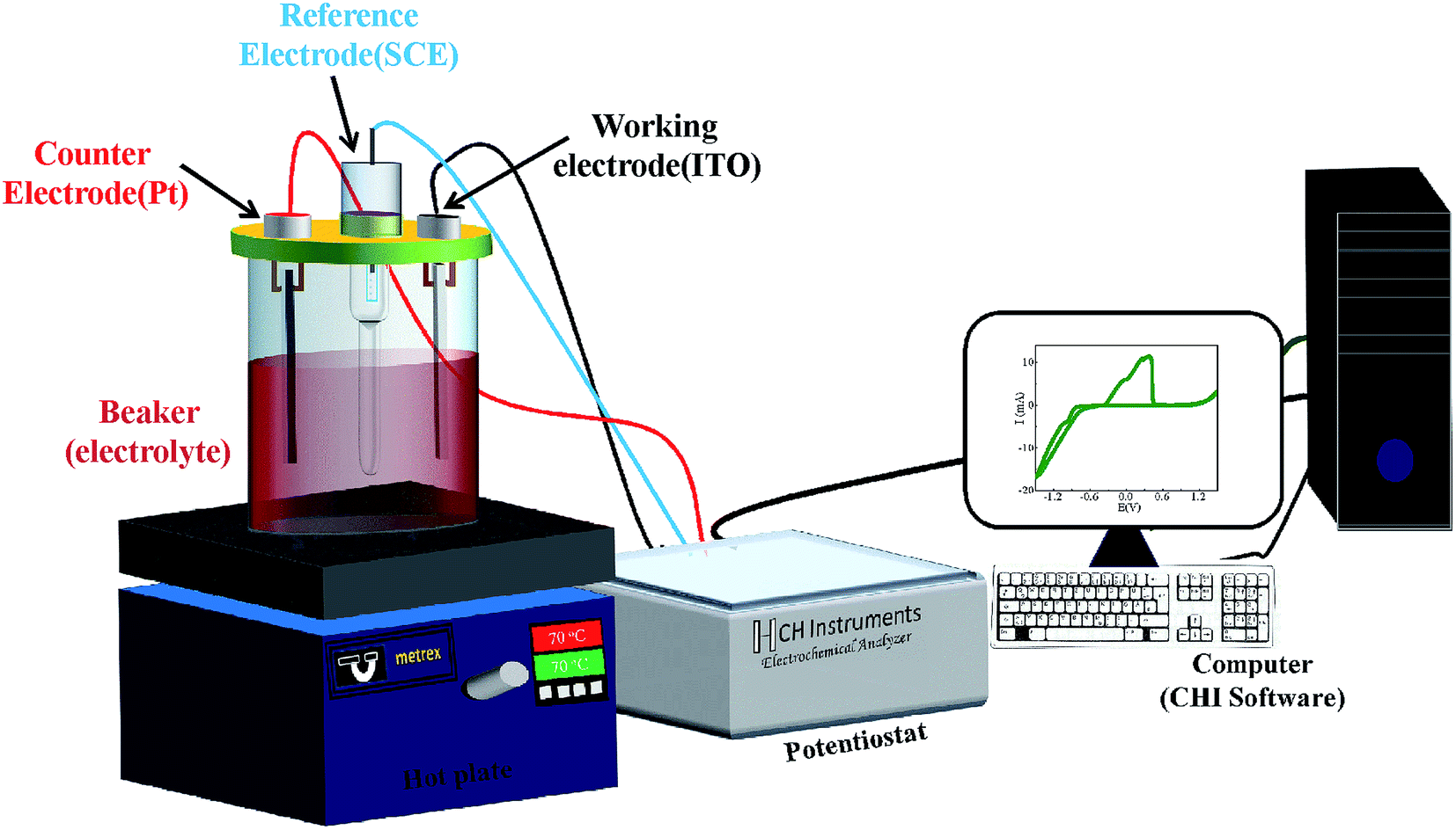
The electrochemical deposition was carried out using computer controlled potentiostat (Model-1140A, CHI make) and CHI software (Fig. 1). A platinum sheet (2.5 × 1 cm2) and saturated calomel electrode SCE (KCl saturated) were used as counter electrode and reference electrode, respectively. The CoSb3 thin films were grown on indium tin oxide (ITO) substrate by varying deposition potential at 70 °C bath temperature. No stirring was used during deposition. Three different sets of samples were deposited under similar conditions to ensure the reproducibility of thermoelectric and other related properties. A Dektak XT surface profiler was used to measure the thickness of the deposited films. As-prepared CoSb3 thin films of typical thickness ∼800 nm were characterized structurally using X-ray diffractometer (PANalytical X'pert Pro model) having CuKα radiation (λ = 1.54 Å) in 2θ range from 20–80° using Bragg–Brentano geometry. Topographic studies were carried out on the substrate and thin films using the Bruker make atomic force microscope (AFM) (Model – Dimension ICON Scan Asyst). Raman spectra were recorded by using Renishaw InVia Micro Raman Spectrometer in 100–300 cm−1 range; utilizing the 532 nm line of Argon ion (Ar+) laser and a 2400 lines per inch grating. The morphology and elemental composition of the deposited films were studied using an analytical scanning electron microscope (SEM, ZEISS EVO 50). A CAMECA IMS-7F magnetic secondary ion mass spectroscopy (SIMS) instrument has been used for elemental depth profiling of the samples. Analysis was performed with a Cs+ primary ion beam of 5 keV impact energy and about 30 nA of beam current. The primary ion beam was raster scanned across a square area of 200 × 200 μm2 of the sample surface. Positive secondary ions, MCs+ (where M is the element to be monitored) were detected from a circular region of 33 μm diameter centered in the rastered area for analysis. Measurements of electrical resistivity and Hall coefficient of the films were carried out at room temperature using van der Pauw method and the Seebeck coefficient was obtained by setting temperature gradient of 5 K between both ends of the sample. The reported electrical parameters have been corrected for the contribution of the conducting substrate.27
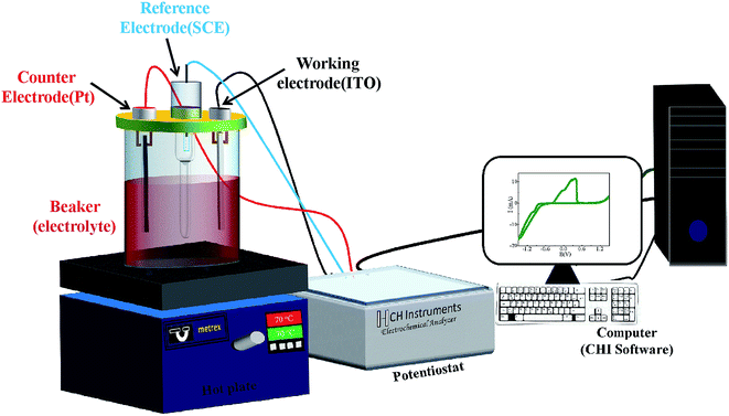 |
| | Fig. 1 Schematic of the electrodeposition set-up. | |
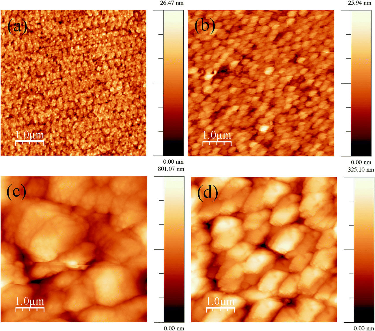
Before each deposition, the ultrasonically cleaned ITO coated glass substrates were subjected to a pre-treatment to improve the surface quality and the reproducibility of the deposition experiments. The pre-treatment consists of cleaning the surface by cycling the potential between −1.5 V and 1.5 V for 5–10 times in the same deposition bath. It has been observed that this treatment is effective in attaining the smooth surfaces, as possible removal of microscopic entities from substrate surface occurs due to cleaning. The quality of the surface was examined by atomic force microscopy (AFM) imaging. The topographical images of substrate and film before and after treatment are shown in Fig. 2(a)–(d) respectively. The significant difference was marked in the surface morphology with respect to the treatment. The appropriate parameter in characterizing the surface morphology of thin films is the rms roughness (ρrms). The ρrms of ITO substrate is 3.3 nm which is decreased to 2.5 nm on pre-treatment. Subsequently, the ρrms of CoSb3 films is found to decrease from 98 nm to 47 nm as a result of pre-treatment.
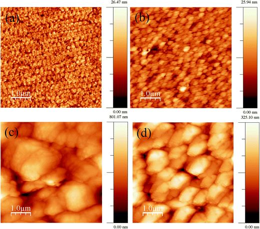 |
| | Fig. 2 Topographical images of (a) untreated ITO substrate, (b) treated ITO substrate, (c) CoSb3 thin film on untreated ITO and (d) CoSb3 thin film on treated ITO substrate. | |
3. Results and discussion
3.1 Cyclic voltammetry (CV)
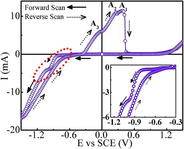
Cyclic voltammetry was carried out to obtain preliminary information regarding the deposition processes and the appropriate deposition potential range. Fig. 3 shows the CV scan recorded at a scan rate of 50 mV s−1 corresponding to 70 °C bath temperature. It is inferred that the peak appearing on the cathodic side at around −0.57 V corresponds to the reduction of Sb3+ ions. The presence of current plateau with low current in the potential range of −0.57 to −0.8 V indicated the diffusion-limited Sb deposition. At −0.8 V the reduction of Co2+ ions commences and thereafter the deposition current increases rapidly and reaches a short plateau region around −0.97 V. On taking the deposition potential beyond −1.0 V, the deposition current continues to increase sharply. Though the co-deposition of Co and Sb initiates at ∼−0.8 V, it seems to stabilize around −0.97 V. The significantly large deposition current after −1.0 V is apparently contributed by Co deposition over Sb deposition. In opposite scan direction, besides the anodic peaks for Co (A3) and Sb (A1) stripping, an oxidation peak (A2) is also observed. This peak is attributed to the interaction between Co and Sb. As the deposition potential can have a strong effect on composition, a series of samples are prepared by taking deposition potentials in different regimes as suggested by CV scan, and tailor stoichiometrically correct composition of CoSb3.
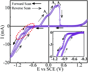 |
| | Fig. 3 Cyclic voltammogram for Co–Sb deposition from pH ∼3 electrolyte bath consisting of 0.003 M Sb2O3, 0.172 M CoSO4·7H2O, 0.125 M sodium citrate and 0.196 M citric acid (inset shows the zoomed view of cathodic scan). | |
3.2 Morphology and composition
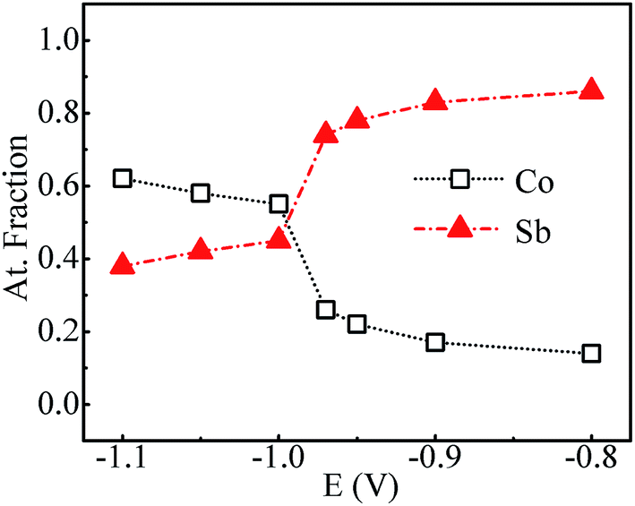
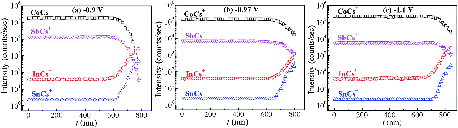
Fig. 4 shows the variation of composition ratio of Co![[thin space (1/6-em)]](https://www.rsc.org/images/entities/char_2009.gif) :Sb in Co–Sb films with deposition potential observed from EDAX data. It is seen that the Co–Sb films are significantly antimony rich at potentials lower than −0.97 V while they become cobalt rich at deposition potentials higher than −0.97 V. The EDAX results showed same trend when repeated on samples deposited a number of times. This trend of composition variation is consistent with the analysis of the CV scans. Thus stoichiometry of the Co–Sb film is very susceptible to the deposition potential, and pure CoSb3 phase is obtained at −0.97 V, which is further confirmed by XRD and Raman data presented later. In order to ascertain the composition uniformity across the thickness, SIMS scans were also recorded on these films. Fig. 5 shows depth profiles of the three representative Co–Sb films deposited at different deposition potentials. A uniform distribution of Co and Sb as a function of sputtering time is clearly seen in these films. This establishes composition stability across the film thickness. The Co and Sb signals drop down (and In and Sn signals from the ITO substrate rise up abruptly) around a depth of ∼700 nm, which is typically the film thickness. Also we notice a change in relative strength of Co and Sb signals, with Co/Sb intensity slightly increasing at higher negative potentials, consistent with the EDAX data analysis that indicates an excess of Sb at lower potentials (<−0.97 V) and an excess of Co at higher potentials (>−0.97 V).
:Sb in Co–Sb films with deposition potential observed from EDAX data. It is seen that the Co–Sb films are significantly antimony rich at potentials lower than −0.97 V while they become cobalt rich at deposition potentials higher than −0.97 V. The EDAX results showed same trend when repeated on samples deposited a number of times. This trend of composition variation is consistent with the analysis of the CV scans. Thus stoichiometry of the Co–Sb film is very susceptible to the deposition potential, and pure CoSb3 phase is obtained at −0.97 V, which is further confirmed by XRD and Raman data presented later. In order to ascertain the composition uniformity across the thickness, SIMS scans were also recorded on these films. Fig. 5 shows depth profiles of the three representative Co–Sb films deposited at different deposition potentials. A uniform distribution of Co and Sb as a function of sputtering time is clearly seen in these films. This establishes composition stability across the film thickness. The Co and Sb signals drop down (and In and Sn signals from the ITO substrate rise up abruptly) around a depth of ∼700 nm, which is typically the film thickness. Also we notice a change in relative strength of Co and Sb signals, with Co/Sb intensity slightly increasing at higher negative potentials, consistent with the EDAX data analysis that indicates an excess of Sb at lower potentials (<−0.97 V) and an excess of Co at higher potentials (>−0.97 V).
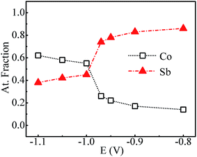 |
| | Fig. 4 Atomic% of Co and Sb in samples prepared at various deposition potentials. | |
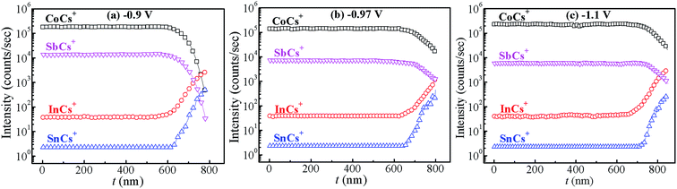 |
| | Fig. 5 SIMS depth profiles recorded on the films prepared at different deposition potentials (a) −0.9 V, (b) −0.97 V and (c) −1.1 V. The signals corresponding to InCs+ and SnCs+ are from the underlying ITO substrate. | |
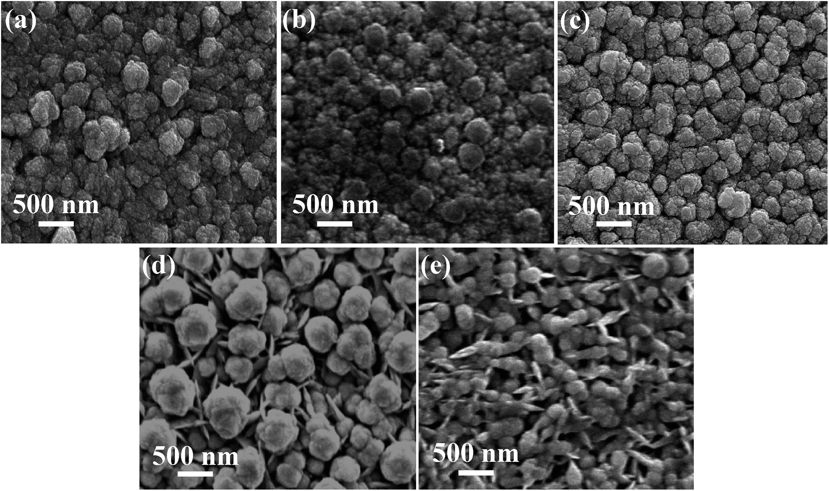
The differences in morphology of the films may be intimately linked to changes in composition and deposition current as deposition potential is varied from −0.8 V to −1.1 V. Fig. 6 shows the SEM images of the films electrodeposited at various potentials. It is clearly seen that the morphology of the films strongly depends on the deposition potential. Fig. 6(a) shows the globular-like grains in the Sb rich Co–Sb films deposited at lower deposition potential (−0.8 V). It is visible that the grain-uniformity enhances with increase in deposition potential. In −0.97 V sample, the smooth surface and narrow globule size variation is observed as compared to the previous two samples. At −1.0 V, the flake/needle like grains start appearing along with globular structure. This transformation from globular to flake-like is more prominent at higher negative potential of −1.1 V. It may be linked to the inclusion of excess Co in the films. A sharp change in morphology at −0.97 V is noticeable in Fig. 6(c), consistent with sharp change in composition at this potential, indicating a very narrow regime of deposition potential for the formation of pure CoSb3 phase, as confirmed later by our XRD and Raman results.
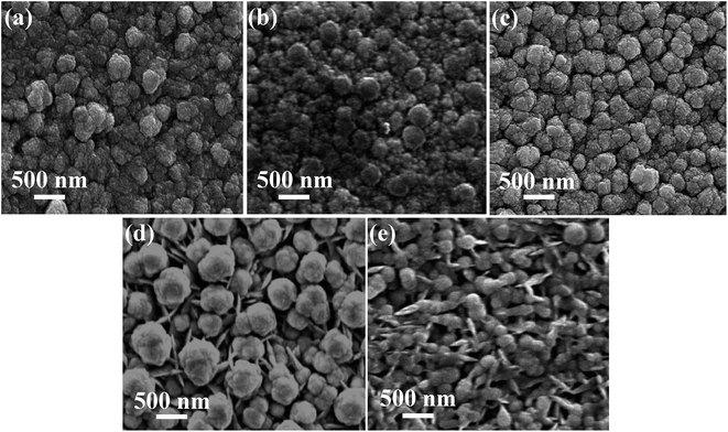 |
| | Fig. 6 (a–e) Surface morphology of CoSb3 thin films deposited at −0.8 V, −0.9 V, −0.97 V, −1.0 V, and −1.1 V deposition potentials respectively. It is clearly noticeable that first the globular grains increase in size attaining near uniform sizes as deposition potential reaches −0.97 V, and thereafter flake-like grains start forming with increasing number density. | |
3.3 Structural behavior
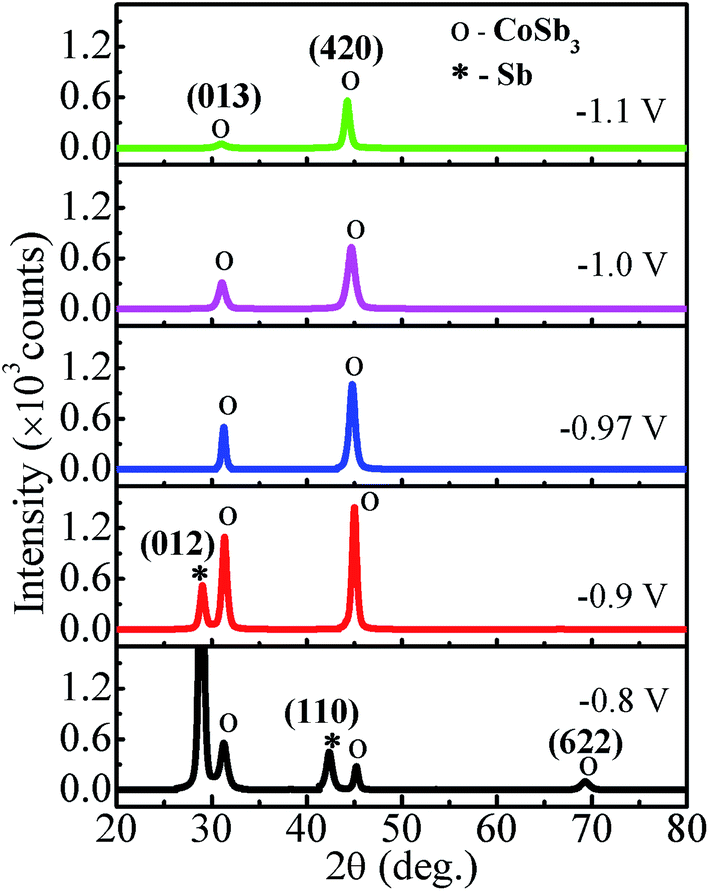
The XRD spectra of Co–Sb films deposited at various deposition potentials −0.8 V, −0.9 V, −0.97 V, −1.0 V, and −1.1 V are shown in Fig. 7. It is clearly seen that the deposition potential has a strong effect on orientation and structural aspect of the films. The high intensity peaks observed in the diffraction spectra confirm the crystalline nature of all the samples. The diffraction data shows the presence of mainly (013) and (420) peaks of the cubic phase of CoSb3 (JCPDS file no. 78-0976). It is further observed that sample deposited at lower deposition potential of −0.8 V exhibits strong peak corresponding to Sb (012), much stronger in intensity than the CoSb3 peaks. The intensity of the (012) peak of Sb phase reduces as the deposition potential is increased to −0.9 V and there is absence of Sb phase in films prepared at −0.97 V and above, consistent with the EDAX data. At −0.97 V, the film possess pure crystalline CoSb3 phase and (420) texture. On further increasing the deposition potential to −1.0 V and −1.1 V, the (013) peak of CoSb3 subsides and films exhibits only (420) peak and that too with much reduced intensity in −1.1 V sample, along with lower crystallite size (see Fig. 8). The overall decrease in intensity of (013) and (420) peaks and decrease in crystallite size with increasing deposition potential may be linked to the sharp rise in deposition current at −1.0 V and the associated increase of Co content in the films. Moreover, the peak position of (420) reflection is found to shift towards lower 2θ values (i.e. from 45.1° to 44.3°) with increase in deposition potential from −0.8 V to −1.1 V. The shift may be understandably attributed to the enhancement of Co concentration in the films with deposition potential as revealed by EDAX studies (Fig. 4). The excess Co may be present either as Co-interstitials sites26 and/or as nano-clusters. Such clusters, if present, are likely to be amorphous/disordered in nature because of which these remain undetected in XRD spectra. Further, the solubility limit of CoSb3 in the Co rich region is larger than that in the Sb rich region,26 and this also provides support to Co remaining undetected and associated (420) peak shift, with Sb being segregated in low deposition potential films.
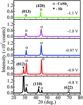 |
| | Fig. 7 XRD patterns of electrodeposited CoSb3 thin films grown at different deposition potentials. | |
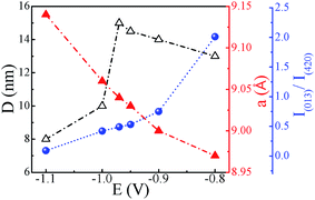 |
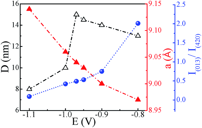
| | Fig. 8 Variation of crystallite size (D), lattice constant (a) and I(013)/I(420) ratio with change in deposition potential (lines serve as guide to the eye). | |
To further study the effect of deposition potential on orientation, the intensity ratio of two prominent peaks (013) and (420) has been compared and the obtained values are plotted in Fig. 8 as a function of deposition potential. The ratio of these two peaks I013/I420 in standard JCPDS (no. 78-0976) is 5. The ratio for −0.8 V sample is found to be 2.0 which signifies that (013) peak is more prominent, whereas for −0.97 V the I013/I420 ratio is 0.5 indicating strong (420) orientation. It is also observed that the full width at half maximum (FWHM) of (420) peak sharply decreases from 0.81° to 0.47° with the deposition potential variation from −0.8 V to −0.97 V. However, at −1.0 V, FWHM is sharply increased to 0.84° and it further increases to 1.10° at −1.1 V. The observed variation in both the parameters (FWHM and intensity) of the diffraction peaks strongly reveals the understandable improved crystallinity of the films at −0.97 V. The excess Sb at lower potentials and excess Co at higher potentials seem to contribute to the decrease in crystallite size and crystallinity of the CoSb3 phase. The crystallite size (D) is estimated using (013) and (420) reflections employing Debye Scherrer formula28 and its variation with deposition potential is shown in Fig. 8. The lattice parameter (a) is calculated from the most intense peak in the XRD spectra. The value of a = 9.04 Å found for −0.97 V exhibits the closest match with the reported value of 9.038 Å.29
It seems that the observed evolution of CoSb3 phase (and its fraction in the film), increase in (420) texturing and the shift of the peak to lower angles can be consistently understood on the basis of the deposition potential controlled variation in relative fluxes of Co and Sb arriving at the substrate (i.e. increase in Co flux relative to the Sb flux that remains diffusion limited). First, the increasing Co flux beyond −0.8 V will result in the formation of stoichiometric CoSb3 phase with improved crystallinity as the Co:Sb fluxes reach a ratio of 1:3 resulting in unhindered and ordered growth of single phase along with columnar and textured grain growth. Then the significant increase of the Co flux, beyond the Co diffusion limited regime of around −0.97 V, will lead to lower crystallite size and reduced crystallinity due to limited surface mobility of ad-atoms caused by high deposition flux and possible formation of second phase due to unbalanced fluxes. Similarly, below −0.97 V the occurrence of unbalanced fluxes causes the segregation of Sb as second phase as seen in XRD data. Second, the relative decrease in Sb flux over the Co flux as we move far away from the Sb deposition potential of −0.57 V, past the Co deposition potential of −0.8 V, causes a relative increase in Co content in the films making them first reach ideal stoichiometry of CoSb3 at deposition potential of −0.97 V, (where Co deposition is also diffusion limited) and then result in films with excess cobalt (as suggested by EDAX of −1.0 V and −1.1 V samples). This argument finds support from the observed shift of the (420) peak from 45.1° to 44.3°, possibly on account of the Co and CoSb3 having higher solubility in Co-rich regime.26 It may be noted that the standard location of (420) CoSb3 peak is 44.8°, which is seen at −0.97 V. Therefore, in turn we can argue that −0.97 V deposited CoSb3 film is stoichiometrically correct, which possibly accounts for their improved TE properties (over −1.0 and −1.1 V films) as seen later.
3.4 Raman spectroscopy
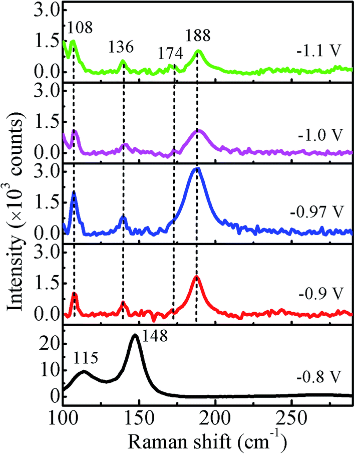
The Raman spectra recorded at room temperature for all the samples in the range of 100–300 cm−1 using the 532 nm excitation line are shown in Fig. 9. For −0.8 V sample, the observed peak at 115 cm−1 corresponds to Eg and that at 148 cm−1 corresponds to A1g vibrational modes of Sb,30 which is consistent with the XRD results. The peaks at 136 cm−1 and 188 cm−1 correspond to Eg and the peak at 108 cm−1 and 174 cm−1 correspond to Fg vibrational modes of CoSb3.31 Thus, the observed peaks in the Raman spectrum of −0.97 V confirm the presence of pure CoSb3 phase. The other two samples deposited at −1.0 V and −1.1 V also show peaks corresponding to CoSb3 phase though with reduced intensity in comparison to −0.97 V. The Raman results are consistent with the good crystalline quality of the films suggested by XRD data. The intensity of all the peaks for −0.97 V sample is highest (more than double) in comparison to other samples, indicating a more ordered local structure/bonding.
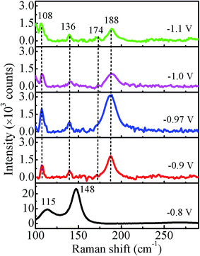 |
| | Fig. 9 Room temperature Raman spectra of CoSb3 films deposited at different deposition potentials. | |
3.5 Electrical behavior
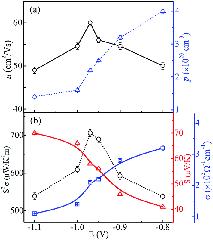
Fig. 10(a) shows the carrier concentration (p) and Hall mobility (μ) of CoSb3 thin films as a function of deposition potential. The obtained parameters are given in Table 1. The value of p across all the samples is found to be ∼1020 cm−3 which is the suitable range to achieve the acceptable thermoelectric properties.1,32,33 The value of p decreases as the deposition potential is varied from −0.8 V to −1.1 V and it has highest value of 4 × 1020 cm−3 at −0.8 V. The segregated metallic Sb phase keeps the p concentration large, though with much smaller mobility, in the −0.8 and −0.9 V films. The p concentration is seen to decrease as deposition potential increases to −0.97 V, consistent with the absence of segregated Sb. Since cobalt interstitials are easily formed in Co rich region and they are p-type,26 the observed very small change in p concentration in the −1.0 V and −1.1 V films is as expected. The value of μ for the sample deposited at −0.97 V has the largest value (60 cm2 V−1 s−1). It may be linked to the presence of pure CoSb3 phase of high crystallinity and/or more ordered local structure, and to the decrease of grain boundaries as the grain size becomes larger. Though the −0.97 V sample has a lower carrier concentration (2.2 × 1020 cm−3) than Sb-rich regime, it has a larger Hall mobility, which results in acceptable thermoelectric properties as presented hereafter. Our value of carrier concentration is about two orders higher than the reported values.29,34
 |
| | Fig. 10 (a) Hole carrier concentration and Hall mobility variation, and (b) power factor, Seebeck coefficient and electrical conductivity variation of CoSb3 thin films as a function of deposition potential (lines serve as guide to the eye). The error bars in the data points show the variation in values obtained for three sets of samples prepared under similar conditions. | |
Table 1 Mean values of all the thermoelectric parameters measured at 300 K of the three sets of CoSb3 thin films deposited at different potentials
| Sample |
σ (ohm−1 cm−1) |
p (cm−3) |
μ (cm2 V−1 s−1) |
S (μV K−1) |
S2σ (μW K−2 m−1) |
| −0.8 V |
3.2 × 10³ |
4.0 × 10²⁰ |
50 |
41 |
538 |
| −0.9 V |
2.8 × 10³ |
3.2 × 10²⁰ |
54 |
46 |
592 |
| −0.95 V |
2.2 × 10³ |
2.5 × 10²⁰ |
56 |
56 |
690 |
| −0.97 V |
2.1 × 10³ |
2.2 × 10²⁰ |
60 |
58 |
706 |
| −1.0 V |
1.4 × 10³ |
1.6 × 10²⁰ |
55 |
66 |
610 |
| −1.1 V |
1.1 × 10³ |
1.4 × 10²⁰ |
51 |
70 |
539 |
The electrical conductivity (σ) varies monotonically from 3.2 × 10³ to 1.1 × 10³ Ω−1 cm−1 with the change in the deposition potential as shown in Fig. 10(b). The decrease in σ can be linked to the lowering in carrier concentration as segregation of metallic Sb subsides, but the decrement in σ is not significant as μ remains high. From EDAX it is observed that cobalt content increases with change in deposition potential to more negative side, but it does lead to increase in carrier concentration as the excess cobalt seems to exist as nano-clusters and/or interstitials, and because of this we see the reduction in p and σ. Such dispersed cobalt causes charge carrier scattering leading to decrease in mobility and an associated increase of Seebeck coefficient, which increases significantly from 41 μV K−1 to 70 μV K−1 as shown in Fig. 10(b). It is observed that the Seebeck coefficient for all the samples possesses positive values (i.e. p-type conduction) which is consistent with the previous reports.34,35 Our observed variations in electrical conductivity and Seebeck coefficient correlate to changes in the morphology, stoichiometry/composition and local atomic order with deposition potential. The globular grains start converting into flake-like structures as more cobalt is there in the films. This overgrowth has negative effect on the transport properties, which can be clearly seen from decrease in mobility values. These variations are attributable to high porosity/smaller grain size and resulting increase in grain boundaries. Moreover, the decrease in carrier concentration results in reduction in electrical conductivity and rise in Seebeck coefficient. It has been reported that the presence of residual metal Sb results in the drop of both electrical resistivity and Seebeck coefficient.36,37 Thus, the lower value of power factor in −0.8 V sample is accountable by the presence of segregated metal Sb. Further, the sample deposited at −0.97 V is more stoichiometric and thus possesses high value of carrier mobility and optimized carrier concentration resulting in higher value of power factor of 706 ± 9 μW K−2 m−1. Table 1 gives the mean values of all the thermoelectric parameters for the three sets of samples prepared at various deposition potentials. The scatter in the data is quite small (see Fig. 10) to clearly bring out the significant variation of each thermoelectric parameter as a function of deposition potential. It is quite noticeable from Fig. 10 that the mobility variation plays the dominant role is deciding the power factor of the film.
Now we compare our results with some recent reports on the p-CoSb3 films and compacted nano-powders in the literature which have largely reported low power factor values at 300 K due to low electrical conductivity and also presumably due to low mobility (though not reported at times) of charge carriers. For example, Zheng et al.35 reported power factor of 95 μW K−2 m−1 in their ion-beam sputtered p-CoSb3 films deposited at 250 °C substrate temperature having comparable S value of 52 μV K but a much lower value of 350 Ω−1 cm−1 for σ and lower mobility of 53 cm2 V−1 s−1. Similarly, solvothermal synthesized p-CoSb3 though shows comparable S of 48 μV K−1 yet shows poor power factor of ∼18 μW K−2 m−1 due to far lower σ of 77 Ω−1 cm−1.38 In yet another report34 on graphene incorporated p-CoSb3 nano-composites, whereas σ shows a five-fold increase to 510 Ω−1 cm−1 and two-fold increase in mobility to 52 cm2 V−1 s−1, the power factor practically shows no change at 300 K (remaining at ∼50 μW K−2 m−1) due to lowering of S value from 69 to 31 μV K−1. However at 800 K the CoSb3/graphene samples show a high power factor of ∼800 μW K−2 m−1. There is a report20 on the formation of n-CoSb3 films by dc sputtering with large S of −140 μV K−1 but with low σ of ∼8 Ω−1 cm−1 and poor power factor of ∼15 μW K−2 m−1. In a recent report39 on amorphous p-CoSb3 films prepared by rf sputtering, good value of power factor (330 μW K−2 m−1) could be obtained at 703 K only after 500 °C annealing induced crystallization. From all these reports we can see that our thermoelectric parameters values at 300 K in as-deposited p-CoSb3 films are a significant improvement and this seems to be on account of improved crystallinity and microstructure quality, and the associated high mobility of charge carriers. In addition the appropriately high enough electrical conductivity (with desirable somewhat low carrier concentration) and high Seebeck coefficient are achieved due to high mobility resulting in high power factor.
4. Conclusions
In summary, we present a hitherto unreported comprehensive and correlated study of the evolution of the Co–Sb system via electrodeposition and it's all the essential physical properties for potential use as thermoelectric material. The controlling influence of deposition potential on the formation of CoSb3 phase and associated thermoelectric properties of electrodeposited CoSb3 thin films has been successfully investigated. With progressively altered microstructure and composition of CoSb3 films we have managed to control hole carrier concentration via stoichiometry and accessed the carrier mobility control via texture and microstructure. Whereas the presence of residual antimony causes lowering of Seebeck coefficient and mobility, its removal by moving to diffusion limited Co deposition regime results in the desired lowering of hole carrier concentration with associated increase in their mobility. Consequently the power factor of the thin films deposited at −0.97 V has a highest value of 706 ± 9 μW K−2 m−1 with a large Seebeck coefficient of 58 μV K−1 and a moderate value of electrical conductivity. The major significance of the work lies in the occurrence of maximized thermoelectric parameters in the as-prepared films without any need of post-deposition annealing or any other treatment, as well as delinked control of carrier concentration and mobility as required in electron-crystal and phonon-glass system.
Acknowledgements
Suchitra Yadav is thankful to MHRD, Government of India for Senior Research Fellowship. We acknowledge the Nanoscale Research Facility (NRF) and Central Research Facility (CRF) at IIT Delhi for AFM and SEM measurements, respectively. We are also thankful to Solid State Physics Laboratory (SSPL), New Delhi for SIMS measurements.
References
- G. J. Snyder and E. S. Toberer, Nat. Mater., 2008, 7, 105–114 CrossRef CAS PubMed.
- J. R. Sootsman, D. Y. Chung and M. G. Kanatzidis, Angew. Chem., Int. Ed. Engl., 2009, 48, 8616–8639 CrossRef CAS PubMed.
- R. Venkatasubramanian, E. Siivola, T. Colpitts and B. O'Quinn, Nature, 2001, 413, 597–602 CrossRef CAS PubMed.
- L. E. Bell, Science, 2008, 321, 1457–1461 CrossRef CAS PubMed.
- M. Ohtaki, T. Tsubota, K. Eguchi and H. Arai, J. Appl. Phys., 1996, 79, 1816–1818 CrossRef CAS.
- S. W. Kim, M. K. Cho, Y. Mishima and D. C. Choi, Intermetallics, 2003, 11, 399–405 CrossRef CAS.
- X. W. Wang, H. Lee, Y. C. Lan, G. H. Zhu, G. Joshi, D. Z. Wang, J. Yang, A. J. Muto, M. Y. Tang, J. Klatsky, S. Song, M. S. Dresselhaus, G. Chen and Z. F. Ren, Appl. Phys. Lett., 2008, 93, 193121 CrossRef.
- H. Fang, Z. Luo, H. Yang and Y. Wu, Nano Lett., 2014, 14, 1153–1157 CrossRef CAS PubMed.
- S. Perumal, S. Roychowdhury and K. Biswas, J. Mater. Chem. C, 2016, 4, 7520–7536 RSC.
- J. F. Li, W. S. Liu, L. D. Zhao and M. Zhou, NPG Asia Mater., 2010, 2, 152–158 CrossRef.
- M. Rull-Bravo, A. Moure, J. F. Fernandez and M. Martin-Gonzalez, RSC Adv., 2015, 5, 41653–41667 RSC.
- C. Uher, Semicond. Semimetals, 2001, 69, 139–253 CrossRef CAS.
- Y. Z. Pei, J. Yang, L. D. Chen, W. Zhang, J. R. Salvador and J. Yang, Appl. Phys. Lett., 2009, 95, 042101 CrossRef.
- X. Li, B. Xu, L. Zhang, F. Duan, X. Yan, J. Yang and Y. Tian, J. Alloys Compd., 2014, 615, 177–180 CrossRef CAS.
- T. B. Massalski, H. Okamoto and P. R. Subramanian, Binary Alloy Phase Diagrams, ASM Intl., 2nd edn, 1990 Search PubMed.
- M. V. Daniel, M. Friedemann, J. Franke and M. Albrecht, Thin Solid Films, 2015, 589, 203–208 CrossRef CAS.
- A. Gharleghi, Y. H. Pai, F. H. Lin and C. J. Liu, J. Mater. Chem. C, 2014, 2, 4213–4220 RSC.
- P. N. Alboni, X. Ji, J. He, N. Gothard and T. M. Tritt, J. Appl. Phys., 2008, 103, 113707 CrossRef.
- S. R. Sarath Kumar, D. Cha and H. N. Alshareef, J. Appl. Phys., 2011, 110, 083710 CrossRef.
- V. Savchuk, A. Boulouz, S. Chakraborty, J. Schumann and H. Vinzelberg, J. Appl. Phys., 2002, 92, 5319–5326 CrossRef CAS.
- F. Xiao, C. Hangarter, B. Yoo, Y. Rheem, K. H. Lee and N. V. Myung, Electrochim. Acta, 2008, 53, 8103–8117 CrossRef CAS.
- H. Cheng, H. H. Hng, J. Ma and X. J. Xu, J. Mater. Res., 2008, 23, 3013–3020 CrossRef CAS.
- D. V. Quach, R. Vidu, J. R. Groza and P. Stroeve, Ind. Eng. Chem. Res., 2010, 49, 11385–11392 CrossRef CAS.
- R. Vidu, S. Li, D. V. Quach and P. Stroeve, J. Appl. Electrochem., 2012, 42, 333–339 CrossRef CAS.
- H. Yamamoto, M. Morishita, Y. Mizuta and A. Masubuchi, Surf. Coat. Technol., 2012, 206, 3415–3420 CrossRef CAS.
- G. Li, S. Bajaj, U. Aydemir, S. Hao, H. Xiao, W. A. Goddard, P. Zhai, Q. Zhang and G. J. Snyder, Chem. Mater., 2016, 28, 2172–2179 CrossRef CAS.
- R. Rostek, J. Kottmeier, M. Kratschmer, G. Blackburn, F. Goldschmidtboing, M. Kroner and P. Woias, J. Electrochem. Soc., 2013, 160, D408–D416 CrossRef CAS.
- N. R. Mathews, C. A. Chávez, M. A. C. Jácome and J. A. T. Antonio, Electrochim. Acta, 2013, 99, 76–84 CrossRef CAS.
- J. Zhang, B. Xu, L. M. Wang, D. Yu, Z. Liu, J. He and Y. Tian, Appl. Phys. Lett., 2011, 98, 072109 CrossRef.
- O. Degtyareva, V. V. Struzhkin and R. J. Hemley, Solid State Commun., 2007, 141, 164–167 CrossRef CAS.
- G. S. Nolas, C. A. Kendziora and H. Takizawa, J. Appl. Phys., 2003, 94, 7440–7444 CrossRef CAS.
- X. Chen, D. Parker, M. H. Du and D. J. Singh, New J. Phys., 2013, 15, 043029 CrossRef.
- A. Shakouri, Annu. Rev. Mater. Res., 2011, 41, 399–431 CrossRef CAS.
- B. Feng, J. Xie, G. Cao, T. Zhu and X. Zhao, J. Mater. Chem. A, 2013, 1, 13111–13119 CAS.
- Z. H. Zheng, P. Fan, G. X. Liang and D. P. Zhang, J. Alloys Compd., 2015, 619, 676–680 CrossRef CAS.
- W. S. Liu, B. P. Zhang, J. F. Li and L. D. Zhao, J. Phys. D: Appl. Phys., 2007, 40, 6784–6790 CrossRef CAS.
- S. Furuyama, T. Iida, S. Matsui, M. Akasaka, K. Nishio and Y. Takanashi, J. Alloys Compd., 2006, 415, 251–256 CrossRef CAS.
- A. Bhaskar, Y. W. Yang, Z. R. Yang, F. H. Lin and C. J. Liu, Ceram. Int., 2015, 41, 7989–7995 CrossRef CAS.
- M. Jeong, A. Ahmed and S. W. Han, Sci. Adv. Mater., 2015, 7, 68–75 CrossRef CAS.
|
| This journal is © The Royal Society of Chemistry 2017 |
Click here to see how this site uses Cookies. View our privacy policy here. 
 Open Access Article
 This Open Access Article is licensed under a Creative Commons Attribution-Non Commercial 3.0 Unported Licence
 a,
Brajesh S. Yadavb,
Sujeet Chaudhary
a,
Brajesh S. Yadavb,
Sujeet Chaudhary