
 Open Access Article
 This Open Access Article is licensed under a
 Creative Commons Attribution 3.0 Unported Licence
Narrow band resonance in the UV light region of a plasmonic nanotextured surface used as a refractive index sensor†
Jingjing Liu‡
 a,
Tengfei Wang‡ab and
Fuqiang Nie*a
a,
Tengfei Wang‡ab and
Fuqiang Nie*a
aDivision of Nanobionic Research, Suzhou Institute of Nano-Tech and Nano-Bionics, Chinese Academy of Sciences, Suzhou 215123, China. E-mail: fqnie2012@sinano.ac.cn; jjliu2015@sinano.ac.cn
bUniversity of Chinese Academy of Sciences, Beijing 100049, China
First published on 19th July 2017
Abstract
We have fabricated two types of plasmonic nanotextured devices (PNDs) using natural lithography technology, which have been applied experimentally in sensing volatile organic solutions (VOS). The PNDs were composed of the hybrid of metal/dielectric structures (PND-1) and metal/dielectric/semiconductor structures (PND-2). They were integrated with microfluidic chips and compared with and without injecting various types of solutions, i.e. DI water, ethanol (C2H5OH), isopropanol (C3H7OH), and ethanediol (C2H4(OH)2). Plasmonic coupling and energy confinement in the PNDs induced a noticeably resonance narrowing of the spectral reflection in the ultra-violet (UV) light region, in which the FWHM (Full-Width at Half-Maximum) was around 20 nm. The experimental results indicate that the sensitivities of the devices are 38.6 nm RIU−1 and 70.8 nm RIU−1 for PND-1 and PND-2, respectively, of which PND-2 is enhanced 1.8-fold compared to PND-1. This sensing approach with high portability, applicability, and cost-effectiveness using plasmonic nanotextured surface based devices may minimize the limitations of time and space in environmental monitoring, food safety and other fields.
1. Introduction
Recently, the optical resonance of metallic nanostructures opens ups avenues for various applications such as chemical or biochemical sensing,1,2 surface-enhanced plasmonic sensing,3 metamaterials,4 optical waveguiding,5 and photonic applications.6 In particular, the metal-dielectric-metal (MDM) multilayer nanostructure by coupling exotic medium is of growing interest.7,8 MDM structures are a class of photonic metamolecules,9 which can support the propagation of the gap plasmon polariton (GPP) mode resulting from the coupling effect of surface polaritons,10,11 which can achieve the subwavelength confinement of light and have important applications in nanoscale optical circuits11 and enhanced optical intensity.12The plasmonic resonance behavior in the visible-light region,7 near-infrared (NIR) region13 and even in the terahertz (THz) region14 have been demonstrated by various metal patterns to enhance the analyte sensitivity, which show that the resonance position is very sensitive on the dielectric surrounding medium.15 In general, researchers have obtained the effective refraction index of patterned perfect metal thin films by means of either the Drude model or direct retrieval from the transmission and reflection coefficients.16 Herein, we report an aperiodic plasmic nanotextured surface with a metal-dielectric-metal (MDM) multilayer nanostructure, which exhibits light–matter interactions overcoming the diffraction limit, enabling the refraction index application in the ultra-violet (UV) regime.
The electromagnetic plasmoic nanotextured surface (PNS) is associated with electric and magnetic fields propagating along a metal–dielectric interface and decaying exponentially in the horizontal and perpendicular directions. Most of the energy is then confined to the metal surface, which explains the remarkable sensitivity of the plasmoic nanotextured surface with respect to changes in the optical parameters at the metal–dielectric boundary.
It is more challenging to detect volatile organic compounds (VOCs) with a small volume or in an unclosed system. Due to VOCs being non-ionic, non-fluorescent and easy to vapourize, the available analytical approaches used for detecting VOCs in microfluidic channels are quite essential. Davidsson et al. developed an ethanol sensor for microfluidic devices using chemiluminescence.17,18 It is a disadvantage that chemiluminescence is needed to be generated by an enzyme. In some other studies, VOCs are detected in an integrated optical Bragg grating refractometer.19 Although these methods do not require additional reagents, precise alignment of the light sources, waveguides, resonators, and detectors on the microfluidic devices are necessary.20 Thus, we have made use of plasmonic nanotextured nanomaterials and their surface sensitivities to demonstrate the refractive index sensing of various chemical solutions in an encapsulated polydimethylsiloxane (PDMS) microfluidic channel, named as plasmonic nanotextured devices (PNDs). The merits of PDMS-based microfluidic systems for biological assays are the reduction of reagent requirements, short analysis times, and portability.21,22 They can be manufactured to possess unique features including inlets, outlets, microvalves, microreactors, micromixers, and various microfluidic chambers. The fabricated microfluidic devices can be assembled in a short period of time without the requirement for expensive design software or clean-room facilities. Therefore, PDMS-based microfluidic systems provide a microenvironment and create a perfect sensing platform for trace chemical detection with several advantages including minimization, portability, minimal use of analytes/reagents and generation of waste, and faster reaction times. Using this technique, samples can be introduced in a continuous flow, allowing for the exposure of a light spot to a sufficient volume of sample.
To avoid the high absorption from water in NIR and middle-infrared (MIR) light regions,23 we explored the proposed PND structures to make the sensing in the near UV light region easily filled into the devices; moreover, in this study, we fabricated a novel plasmonic device working as a refractive index (RI) sensor for the 250–350 nm wavelength range, which is the first device for the ultra-violet (UV) light region.
2. Materials and methods
Fig. 1 shows the flow process used for the fabrication of the PNDs using natural lithography technology. First, SiO2 and gold (Au) thin-films with a thickness of 150/50 nm were deposited on a (100) n-type Si substrate using low-temperature chemical vapor deposition (LPCVD) and electron-beam evaporation, respectively, as shown in Fig. 1(a). Second, the sample was annealed at 800 °C at 250 mTorr in an Ar atmosphere for 20 min to form Au nanoparticles with a grain size in the range of 100–150 nm (Fig. 1(b)). Each island (i.e. grain) of the Au nanoparticles functioned as an individual hard mask for subsequent etching. The sample was vertically etched on the SiO2 thin-film surface using a mixed gas of SF6/CHF3 at 130 sccm via reactive ion etching (RIE) at 5 mTorr and a source power of 80 W for 1 min as shown in Fig. 1(c). Thus far, the devices were composed of metal/dielectric structures and denoted as PND-1. Sequentially, the samples were etched on the Si substrate with SF6 gas at 15 sccm via RIE at 1000 mTorr for 120 s to form the metal/dielectric/semiconductor structures as shown in Fig. 1(d), denoted as PND-2. | ||
| Fig. 1 The flow process used for the fabrication of the PNDs. (a) SiO2 and Au thin-films were deposited on a (100) n-type Si substrate. (b) The samples were annealed at 800 °C. (c) The samples were patterned by etching SiO2 to form the metal/dielectric structures. (d) The samples were patterned by etching Si to form the metal/dielectric/semiconductor structures. | ||
To verify the VOS sensing characteristics using PND-1 and PND-2, the devices were encapsulated in a PDMS-based microfluidic channel and characterized using a UV-vis spectrometer (Ocean Optics Ltd. Co., Maya2000 Pro.). The fabrication process of the PDMS-based microfluidic system is illustrated as follows. PDMS prepolymer and curing agent (10![[thin space (1/6-em)]](https://www.rsc.org/images/entities/char_2009.gif) :1 w/w, Sylgard 184, Dow-Corning) were mixed at a 10:1 ratio and degassed under vacuum for 30 min. The mixture was poured over an SU-8 mold (thickness: 1 mm, length: 10 mm, width: 10 mm) on a glass slide (length: 76.2 mm; width: 25.4 mm) master and then baked at 80 °C for 1 h to create the microchannel. After curing, a piece of PDMS microchannel was formed and peeled from the glass master. To complete the fabrication of the sensing system, the PDMS microchannel was drilled with holes, 5 mm in diameter for the inlet and outlet of the microfluidic system, and then plasma bonded to the Si substrate containing the pre-patterned plasmonic nanotextured surface. Finally, it was assembled with appropriate connectors, such as Tyron tubes, syringe, and syringe pump to form a microfluidic system. A schematic of the experimental set-up is shown in Fig. 2. The inlet and outlet of the PDMS fluidic channel were formed by having Tyron tubes inserted for sample delivery. The fluidic channel was connected to a syringe, via an inlet tube, and syringe pump, which was used to drive the various VOS alternately. The injected volume was kept at 100 μL with a flow rate of 1 mL min−1 for all the VOS. These liquids give a good spread of refraction index values, enabling us to investigate the sensitivities of the plasmonic sensing with various VOS samples.
:1 w/w, Sylgard 184, Dow-Corning) were mixed at a 10:1 ratio and degassed under vacuum for 30 min. The mixture was poured over an SU-8 mold (thickness: 1 mm, length: 10 mm, width: 10 mm) on a glass slide (length: 76.2 mm; width: 25.4 mm) master and then baked at 80 °C for 1 h to create the microchannel. After curing, a piece of PDMS microchannel was formed and peeled from the glass master. To complete the fabrication of the sensing system, the PDMS microchannel was drilled with holes, 5 mm in diameter for the inlet and outlet of the microfluidic system, and then plasma bonded to the Si substrate containing the pre-patterned plasmonic nanotextured surface. Finally, it was assembled with appropriate connectors, such as Tyron tubes, syringe, and syringe pump to form a microfluidic system. A schematic of the experimental set-up is shown in Fig. 2. The inlet and outlet of the PDMS fluidic channel were formed by having Tyron tubes inserted for sample delivery. The fluidic channel was connected to a syringe, via an inlet tube, and syringe pump, which was used to drive the various VOS alternately. The injected volume was kept at 100 μL with a flow rate of 1 mL min−1 for all the VOS. These liquids give a good spread of refraction index values, enabling us to investigate the sensitivities of the plasmonic sensing with various VOS samples.
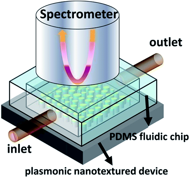 | ||
| Fig. 2 A schematic of the microfluidic measurement set-up. | ||
3. Results and discussion
Fig. 3 shows the cross-sectional views of the PNDs using field-emission scanning electron microscopy (SEM) system. It can be seen that the aperiodic nanostructures were distributed uniformly after the fabrication process for PND-1 and PND-2 as shown in Fig. 3(a) and (b), respectively. Fig. 3(c) and (d) show the cross-sectional SEM images in which the aperiodic nanostructures were measured to be in the period ranges of ∼300 nm and ∼500 nm in depth for PND-1 and PND-2, respectively. The multi-layers clearly show the nanostructures of PND-1 and PND-2 composed of the metal/dielectric and metal/dielectric/semiconductor structures. The height of the etched SiO2 in PND-1 is 150 nm as denoted by both L1 and L2 in Fig. 3(c) and (d), respectively.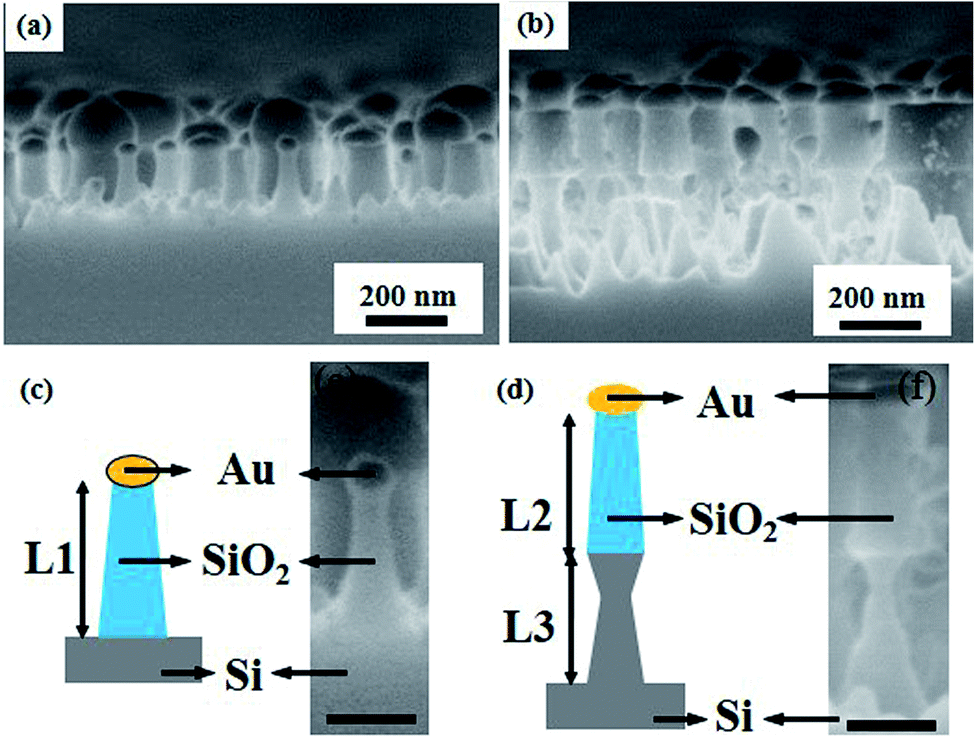 | ||
| Fig. 3 (a) and (b) are the top SEM images and (c) and (d) are the cross-sectional SEM images of PND-1 and PND-2, respectively. (e) and (f) are the corresponding unit nanostructural geometries of PND-1 and PND-2, respectively, where the scale bar is 100 nm. | ||
In our nanostructures, the dielectric layer of SiO2 in the medium structure can highly enhance the local electromagnetic intensity around the plasmonic Au NPs. In the wavelength region from 250–400 nm, two resonant peaks were found in PND-2 while a single resonant peak was found in PND-1, resulting from the two types of surface plasmons between the two nanotextured surfaces. The first type may be generated by the Au nanoparticles, which could be excited by light to oscillate at the interface. Conduction electrons in metal nanomaterials could be coherently excited by incident light to oscillate collectively at metal/dielectric interfaces.24 As can be seen from Fig. 4, the first resonant peak_1 in PND-2 is weaker than the resonant peak in PND-1 and a little blue-shift is observed. The lower intensity of reflective of peak_1 in PND-2 could be explained by the deeper etching condition with around 500 nm of the total height; moreover, the blue-shift is also known to be caused by the deeper structure.25 The SiO2/Si, which is the dielectric/semiconductor layer, may give rise to the second type of surface plasmon, which is shown in Fig. 4 as peak_2 in PND-2.
 | ||
| Fig. 4 The shift in the resonant wavelength of the PND-1 device (a) and PND-2 device (b) in various chemical solutions, respectively. | ||
Fig. 4 shows the experimental results of the PND-1 and PND-2 devices under various VOS. As can be seen, there is a significant red-shift at the resonances as the refraction index (RI) of the fluid filling the PDMS-based microchannel increases. In the absence of a chemical solution, i.e., n = 1 (ambient air), the resonance is 312.5 nm for PND-1, while the two orders of PND-2 are located at 282.2 nm and 351.8 nm. When the microfluidic channel was injected with DI water, ethanol, isopropanol, and ethanediol, the resonances were shifted from 312.2 nm (air) to 315.2 nm (water), 312.2 nm (air) to 320.1 nm (ethanol), 312.2 nm (air) to 321.2 nm (IPA) and 312.5 nm (air) to 329.9 nm (ethanediol) for PND-1. Fig. 5 gives the resonance intensity variations among the different media or solution for peak_1 and peak_2 of PND-2. It is interesting that the variation of the resonances for the two peaks tend to approach the RI value increasing with the different chemical solutions. To further investigate the VOS sensing capabilities of PND-1 and PND-2, a C2H4(OH)2 solution at different concentrations was chosen and injected into the PDMS-based microfluidic channel (Fig. S1, ESI†).
 | ||
| Fig. 5 The variation in the resonant intensity among different media or solution for peak_1 and peak_2 of PND-2. | ||
To clarify the sensitive capability of PNDs, the resonant shifting of the various chemical solutions was plotted against their respective refractive indices in Fig. 6. Notably, the RI values vary as the wavelength changes; thus, after a slit resonant shift, the RI value will be altered sequentially. We added the range of the RI change, which we referred to from the website of the refractive index database.26 Apparently, PND-2 shows a larger resonant shift than PND-1. Furthermore, the maximum resonant shift was 31.7 nm, which is larger than the reported resonant RI shift of 15 nm.27
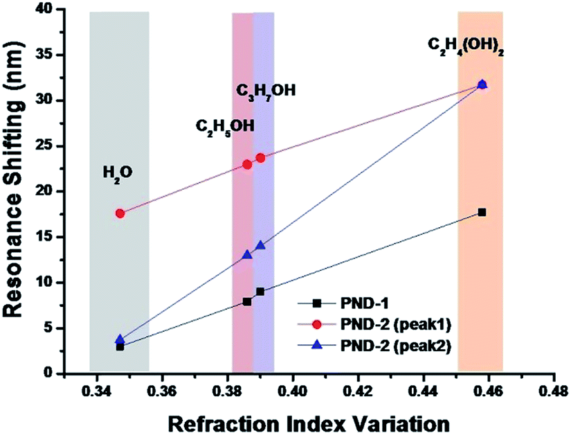 | ||
| Fig. 6 The relationship between the variation in refractive index and shift in the resonance of PND-1 and PND-2 (the refraction index value refers to database26). | ||
The sensitivity (nm RIU−1) of the plasmonic nanotextured device is the shift in the resonant wavelength per unit change of the refraction index. Table 1 summarizes the sensing performance of the PNDs used as a refractive index sensor. Comparing the sensitivity (nm RIU−1) of peak_1 and peak_2 of PND-2 and PND-1, they are from 50.4 nm RIU−1 to 68.6 nm RIU−1 for peak_1 of PND-2, from 10.8 nm RIU−1 to 70.8 nm RIU −1 for peak_2 of PND-2, and 8.6 nm RIU−1 to 38.6 nm RIU−1, respectively. This shows that peak_1 of PND-2 improved the sensitivity around 1.6-fold and 2.5-fold on average better than that of peak_2 of PND-2 and PND-1, respectively. For sensing different concentrations of C2H4(OH)2, the performance of the sensitivities are summarized in Table S1 (ESI†). A significant narrow FWHM (Full-Width at Half-Maximum) was found in our study: ∼28 nm for PND-1, ∼20 nm for peak_1 of PND-2 and ∼30 nm for peak_2 of PND-2. This indicates that low energy losses excited from plasmon resonant are contributed by the aperiodic structure.28 Moreover, the coupling deeper structures of PND-2 with metal/dielectric/semiconductor show the sharp FHMW ∼20 nm for peak_1. PND-2 shows a high sensitivity that might be attributed MDM, resulting from the coupling effect of surface waves. It will further prove that the hybridized resonance can enhance the field confinement of the reflected light.25 According to the standing-wave resonance mode, energy confinement in the nanocavity can arouse a significant resonance narrowing.25
| Solution | Resonant shift (Δ) | FWHM | Sensitivity (nm RIU−1) | FOM | |
|---|---|---|---|---|---|
| PND-1 | |||||
| H2O | 3 | 29 | 8.6 | 0.3 | |
| C2H5OH | 7.9 | 28 | 20.5 | 0.7 | |
| C3H7OH | 9 | 28 | 22.5 | 0.8 | |
| C2H4(OH)2 | 17.7 | 29 | 38.6 | 1.3 | |
|
|||||
| PND-2 (peak_1) | |||||
| H2O | 17.6 | 19 | 50.4 | 2.7 | |
| C2H5OH | 21.2 | 19 | 54.5 | 2.9 | |
| C3H7OH | 23.7 | 21 | 58.2 | 2.8 | |
| C2H4(OH)2 | 31.7 | 22 | 68.6 | 3.1 | |
|
|||||
| PND-2 (peak_2) | |||||
| H2O | 3.7 | 32 | 10.8 | 0.3 | |
| C2H5OH | 10.3 | 31 | 27.2 | 0.9 | |
| C3H7OH | 14 | 31 | 35.4 | 1.1 | |
| C2H4(OH)2 | 31.7 | 37 | 70.8 | 1.9 | |
In order to provide better quantification, the figure-of-merit (FOM) is another important factor used to determine the capability of a chemical sensor. It is defined as the sensitivity value divided by the resonance line width at half-maximum, i.e. FOM = (Δλ/Δn)/FWHM, where Δλ/Δn is the change in the resonant wavelength per refraction, index unit and the FWHM is the full width at half maximum of the resonance.29 This FOM was calculated for each sample to evaluate the performance of the devices for refraction index sensing. Correspondingly, we can obtain the highest value of FOM as 3.1, for peak_1 of PND-2 sensing ethanediol, which is around 2.3-fold higher than PND-1, and around 1.6-fold higher than peak_2 of PND-2 sensing the same chemical solution, respectively. Finally, we demonstrated that our PND devices may serve as highly efficient plasmonic sensors in the 250–400 nm wavelength range.
In conclusion, we have demonstrated an effective chemical sensing approach using a plasmoic nanotextured surface integrated with a PDMS fluidic channel platform. The PND design has two major advantages. First, it can be easily fabricated using natural lithography technology. Second, the sensing medium is easily filled into the voids for plasmonic resonance sensor applications. Therefore, it facilitates the detection of refraction index changes. The experimental results indicate the feasibility of refraction index detection for different chemical solutions. This indicates a creation of a remote optical sensing mechanism using the chemical solutions with different refraction indexes to adjust the resonant wavelength of the PNDs. An ultra-narrow FHMW of ∼20 nm was found in peak_1 of PND-2, indicating that the coupling deeper structures of with metal/dielectric/semiconductor can improve the sensitivity. We believe that our MDM nanostructures can be exploited for further applications in enhanced spectroscopy.
Acknowledgements
This study is financial supported by the Jiangsu Natural Science Youth Foundation (No. BK20160398) and Suzhou Science and Technology Project (No. SYG201633).References
- Y. Tian, et al., An Individual Nanocube-Based Plasmonic Biosensor for Real-Time Monitoring the Structural Switch of the Telomeric G-Quadruplex, Small, 2016, 12(21), 2913–2920 CrossRef CAS PubMed.
- M. T. Do, et al., Fabrication and Characterization of Large-Area Unpatterned and Patterned Plasmonic Gold Nanostructures, J. Electron. Mater., 2016, 45(5), 2347–2353 CrossRef CAS.
- M. Abb, et al., Surface-enhanced infrared spectroscopy using metal oxide plasmonic antenna arrays, Nano Lett., 2014, 14(1), 346–352 CrossRef CAS PubMed.
- S. A. Gregory, et al., Extreme Subwavelength Metal Oxide Direct and Complementary Metamaterials, ACS Photonics, 2015, 2(5), 606–614 CrossRef CAS.
- M. Fevrier, et al., Giant coupling effect between metal nanoparticle chain and optical waveguide, Nano Lett., 2012, 12(2), 1032–1037 CrossRef CAS PubMed.
- C. Lin, et al., Oxyfluoride Glass-Ceramics for Transition Metal Ion Based Photonics: Broadband Near-IR Luminescence of Nickel Ion Dopant and Nanocrystallization Mechanism, J. Phys. Chem. C, 2016, 120(8), 4556–4563 CAS.
- J. Fan, et al., Standing-wave resonances in plasmonic nanoumberllar cavities for color generation and colorimetric refractive index sensor, Appl. Surf. Sci., 2016, 384, 534–538 CrossRef CAS.
- J. Chen, et al., Coupling between gap plasmon polariton and magnetic polariton in a metallic-dielectric multilayer structure, Phys. Rev. E: Stat., Nonlinear, Soft Matter Phys., 2011, 84, 026603 CrossRef PubMed.
- C. Tserkezis, et al., Understanding artificial optical magnetism of periodic metal-dielectric-metal layered structures, Phys. Rev. B: Condens. Matter Mater. Phys., 2008, 78(16), 165114 CrossRef.
- K. Park, et al., Study of the surface and bulk polaritons with a negative index metamaterial, J. Opt. Soc. Am. B, 2005, 22(5), 1016–1022 CrossRef CAS.
- K. Tanaka and M. Tanaka, Simulations of nanometric optical circuits based on surface plasmon polariton gap waveguide, Appl. Phys. Lett., 2003, 82(8), 1158 CrossRef CAS.
- J. Chen, et al., Optical bistability enhanced by highly localized bulk plasmon polariton modes in subwavelength metal-nonlinear dielectric multilayer structure, Appl. Phys. Lett., 2009, 94(8), 081117 CrossRef.
- M. D. keshav, et al., Subpicosecond optical switching with a negative index metamaterial, Nano Lett., 2009, 9(10), 3565–3569 CrossRef PubMed.
- D. K. Polyushkin, et al., THz generation from plasmonic nanoparticle arrays, Nano Lett., 2011, 11(11), 4718–4724 CrossRef CAS PubMed.
- N. Liu, et al., Planar metamaterial analogue of electromagnetically induced transparency for plasmonic sensing, Nano Lett., 2010, 10(4), 1103–1107 CrossRef CAS PubMed.
- M. Ren, et al., Isotropic spiral plasmonic metamaterial for sensing large refractive index change, Opt. Lett., 2013, 38(16), 3133–3136 CrossRef PubMed.
- R. Davidsson, et al., Microfluidic biosensing systems. Part I. Development and optimisation of enzymatic chemiluminescent micro-biosensors based on silicon microchips, Lab Chip, 2004, 4(5), 481–487 RSC.
- C. F. Carlborg, et al., A packaged optical slot-waveguide ring resonator sensor array for multiplex label-free assays in labs-on-chips, Lab Chip, 2010, 10(3), 281–290 RSC.
- D. J. Wales, et al., An integrated optical bragg grating refractometer for volatile organic compound detection, Sens. Actuators, B, 2016, 232, 595–604 CrossRef CAS.
- P. S. Nunes, et al., Refractive index sensor based on a 1D photonic crystal in a microfluidic channel, Sensors, 2010, 10(3), 2348–2358 CrossRef CAS PubMed.
- H. Somaweera, A. Ibraguimov and D. Pappas, A review of chemical gradient systems for cell analysis, Anal. Chim. Acta, 2016, 907, 7–17 CrossRef CAS PubMed.
- S. G. M. Uzel, et al., Simultaneous or Sequential Orthogonal Gradient Formation in a 3D Cell Culture Microfluidic Platform, Small, 2016, 12(5), 612–622 CrossRef CAS PubMed.
- J. Xu, K. W. Plaxco and S. J. Allen, Absorption spectra of liquid water and aqueous buffers between 0.3 and 3.72 THz, J. Chem. Phys., 2006, 124(3), 036101 CrossRef PubMed.
- S.-Y. Ding, et al., Nanostructure-based plasmon-enhanced Raman spectroscopy for surface analysis of materials, Nat. Rev. Mater., 2016, 1(6), 16021 CrossRef CAS.
- J. Fan, et al., Standing-wave resonances in plasmonic nanoumbrella cavities for color generation and colorimetric refractive index sensor, Appl. Surf. Sci., 2016, 384, 534–538 CrossRef CAS.
- http://www.refractiveindex.info/?shelf=organic%26book=ethanol%26page=Sani.
- S. G. Uzel, et al., Simultaneous or Sequential Orthogonal Gradient Formation in a 3D Cell Culture Microfluidic Platform, Small, 2016, 12(5), 612–622 CrossRef CAS PubMed.
- Y. Li, et al., Phase Separation of Silicon-Containing Polymer/Polystyrene Blends in Spin-Coated Films, Langmuir, 2016, 32(15), 3670–3678 CrossRef CAS PubMed.
- L. J. Sherry, et al., Localized surface plasmon resonance spectroscopy of single silver nanocubes, Nano Lett., 2005, 5(10), 2034–2038 CrossRef CAS PubMed.
Footnotes |
| † Electronic supplementary information (ESI) available. See DOI: 10.1039/c7ra01642e |
| ‡ These authors contributed equally. |
| This journal is © The Royal Society of Chemistry 2017 |