
 Open Access Article
 This Open Access Article is licensed under a
 Creative Commons Attribution 3.0 Unported Licence
Formation of C60 fullerene-bonded-CNTs using radio frequency plasma†
Shengxia Duanab,
Xia Liuab,
Yanan Wangab,
Dadong Shaoa,
Yuedong Menga,
Tasawar Hayatde,
Ahmed Alsaedid and
Jiaxing Li *acd
*acd
aInstitute of Plasma Physics, Chinese Academy of Sciences, P.O. Box 1126, Hefei 230031, P. R. China. E-mail: lijx@ipp.ac.cn; Tel: +86 65596617
bUniversity of Science and Technology of China, Hefei, 230026, P. R. China
cCollaborative Innovation Center of Radiation Medicine of Jiangsu Higher Education Institutions, P. R. China
dNAAM Research Group, King Abdulaziz University, Jeddah, 21589, Saudi Arabia
eDepartment of Mathematics, Quaid-I-Azam University, Islamabad 44000, Pakistan
First published on 12th April 2017
Abstract
C60 fullerene-bonded-CNTs (CNBs) were successfully synthesized by radio frequency plasma (RF plasma) treatment for the first time. High-resolution transmission electron microscopy (HRTEM) and Raman spectroscopy were used to confirm the formation of the CNB structure. A possible mechanism was also proposed to explain the formation of CNBs. This RF plasma treatment may inspire a novel method to potentially overcome the synthetic difficulty of CNBs.
Hybrid carbon nanostructures integrating 0-dimensional (0D) fullerenes, 1D carbon nanotubes (CNTs), and 2D graphene can afford a compelling possibility to combine the great characteristics of individual carbon nano-allotropes in a selective manner.1 The first hybrid carbon material, named the carbon nano-peapod, was discovered in 1998 by Smith et al.,2 in which the fullerene molecules are encapsulated in CNTs (a schematic representation of the carbon nano-peapod is shown in Fig. S1†). After that, great contributions have been made to investigating the formation of carbon nano-peapods.3,4 For instance, Luzzi et al. synthesized carbon nano-peapods from single-walled and double-walled nanotubes grown by a chemical vapor deposition (CVD) method.3 Shen also utilized the molecular dynamics (MD) method to simulate the compression and tension of the carbon nano-peapod.4 Besides carbon nano-peapod materials, carbon nanobuds (CNBs), a novel fullerene–CNT hybrid nanostructure, formed by fullerene units covalently attached to CNTs, have attracted increasing attention both experimentally and theoretically. Typically, nanobuds have been prepared by aerosol (floating catalyst) CVD method based on CO decomposition on iron particles produced from ferrocene vapour, shown in Scheme S1.†5 The first experimentally obtained CNBs was reported by Kauppinen et al. via a ferrocene vapour decomposition.6 The presence of C20, C42 and C60 fullerene units covalently bonded to the outer surface of the CNTs. The obtained CNBs exhibited enhanced cold electron field-emission properties.6 Nicholls et al. also synthesized CNBs through a CVD method and indicated that CNBs can be utilized as a precursor in the synthetic process of nanotube junction.7 In addition to experimental studies, theoretical studies based on density functional theory (DFT) method were also carried out to investigate the properties of CNBs in various aspects,8 such as its relative reactivity towards amine nucleophile8d and its Raman features of the CNBs.8e
The strong covalent bonding between fullerenes and CNTs in CNBs could provide the advantageous properties to this hybrid material that are unavailable for nano-peapods, such as transport, magnetism, electricity and optical limiting performance. For instance, the carbon nanomaterial prepared by Nasibulin et al. exhibit a low field threshold of about 0.65 V μm−1 and a much higher current density compared with pure SWNTs.6a Additionally, the optical limiting performance of CNBs is found to be superior to that of SWNTs reported by Wang et al.9 Although the above studies provided detailed investigation on the synthesis, configuration and physicochemical properties for CNBs, the experimental synthesis of CNBs is still limited and the commonly used CVD method also suffers its disadvantages, such as high operating temperature, toxic CO gas and specific reaction pressure, resulting in an inconvenient operation. Thus, it is necessary to explore new approach to synthesize CNBs with stable configuration, such as straightforward synthesis, convenient and environmental friendly process. RF (radio frequency) plasma treatment can be utilized as a novel alternative toward traditional CVD method to prepare CNBs by generating chemical active species. Virtually, all solid materials can be treated by this method with no solvent involved in the process, thus, producing no waste.10 Meanwhile, previous reports have exhibited successful fabrication of CNTs anchored with various agents by this RF plasma treatment method.11 Thus, in this study, we reported the synthesis of CNBs by RF plasma treatment for the first time as an easy operation, high efficient, economic and environmental benign process. Moreover, the C60 fullerene-bonded-CNT is still referred to as CNBs due to its similar appearance with CNBs obtained by CVD method. Additionally, to better understand the benefit of RF plasma treatment method, a clearer explanation of the CVD method was given in ESI,† accompanying with a schematic presentation of CVD method.
Fig. 1 illustrates the schematic view of the experiment setup, which mainly consists of one three-necked, round-bottom flask with winding coils and a pulsed dc power supply (a whole schematic view of the experiment setup was shown in Fig. S2†). The plasma coil served as a high-voltage (HV) electrode and directly connected to the pulsed dc power supply. Firstly, a 1![[thin space (1/6-em)]](https://www.rsc.org/images/entities/char_2009.gif) :1 ratio (by mass) of CNTs and fullerene (C60) were mixed and grinded, which were subsequently transferred to the round bottom flask. The HV pulsed dc power with 100 W was applied to the plasma coil until N2 vacuum degree of the glass flask reached a relative stable state of ∼3.9 Pa. The CNT/fullerene mixtures were treated under this condition for about 1 h before injecting 20 mL carbon disulphide (CS2) into the round bottom flask. Finally, the whole mixture was continuously stirred for ∼24 h under ambient temperature after which the sample was collected and washed several times with CS2 to remove the unreacted C60. With no extra post-synthetic process, the purified sample was dried in a vacuum oven at 60 °C for 12 h to obtain the desired CNBs.
:1 ratio (by mass) of CNTs and fullerene (C60) were mixed and grinded, which were subsequently transferred to the round bottom flask. The HV pulsed dc power with 100 W was applied to the plasma coil until N2 vacuum degree of the glass flask reached a relative stable state of ∼3.9 Pa. The CNT/fullerene mixtures were treated under this condition for about 1 h before injecting 20 mL carbon disulphide (CS2) into the round bottom flask. Finally, the whole mixture was continuously stirred for ∼24 h under ambient temperature after which the sample was collected and washed several times with CS2 to remove the unreacted C60. With no extra post-synthetic process, the purified sample was dried in a vacuum oven at 60 °C for 12 h to obtain the desired CNBs.
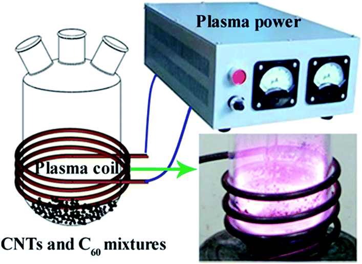 | ||
| Fig. 1 Schematic view of the experiment setup. | ||
The produced CNBs structure was confirmed by HRTEM and Raman spectroscopy. Since the inherent vibration of CNBs during the electron beam penetration process, it is challenging to obtain clear TEM images of CNBs, as shown in Fig. 2 for both CNTs and CNBs. CNTs with C60 of various sizes were presented and this observation is consistent with the previously reported results.6,7,12 Fig. 2a and b clearly demonstrated a smooth surface of CNTs with a diameter of ∼5 nm. However, after RF plasma treatment, a rough surface of CNBs was observed (Fig. 2c and d), which can be attributed to the micro-etch formations by RF plasma treatment and the addition of C60 (the spherical dots) on the surface of CNTs. The diameter of single modified C60 is measured to be about 1 nm, 1/5 of the CNTs diameter. However, the distribution of modified C60 on the CNTs surface is not uniform, due to the destruction of C60 and the formation of fullerene dimers or oligomers under the plasma treatment. Moreover, RF treatment time was varied as 30 min and 120 min to investigate effect of treatment time on the density of the buds. And the corresponding HRTEM images of CNBs were given in Fig. S4.† It can be seen that the RF treatment time has little effect on the density of the buds. In addition to varying the RF treatment time, impact of ratios of C60:CNTs on the outcomes of the carbon structures was also investigated. Although it is fallacious to compare the outcomes of the carbon structures via varying the ratios of C60:CNTs due to the uneven grind, it is still can be found that the density of buds increases with the increase of C60:CNTs ratios from 0.5 to 2, shown in Fig. S5.† In spite of the density increase resulted from the higher mass ratio of C60:CNTs, CNBs obtained from the ratio of 1:1 was still chosen to make the discussion considering the relative high density of buds and cost savings. Additionally, increasing the yield of CNBs is still under processing. Moreover, the raw CNTs and C60 fullerenes were exposed to the RF plasma treatment for 1 h. And the corresponding TEM images were given in Fig. S6 and S7,† respectively. It can be seen that the overall morphologies of CNTs did not change after RF plasma treatment except the appearance of rough surface due to the micro-etch formations resulted from the RF plasma treatment. Moreover, the plasma treatment can produce chemically active species on the surface of the substrate and have no effect on its inner structure, thus, plasma treatment does not lead to interesting surface structures. Without attaching to the CNTs surface, the C60 fullerenes after plasma treatment tend to agglomerate, since C60 fullerenes are known to be easily polymerized upon application of external energy sources, such as electron beams or photons.13 And clusters of C60 fullerenes are clearly observed in an aggregated state (Fig. S7a†). Additionally, typical HRTEM image of the fullerene cluster is shown in Fig. S7b.† The images clearly show that the C60 fullerenes are polycrystalline in nature, which is supposedly most free from the confusion because of the projection of overlapping structures.14
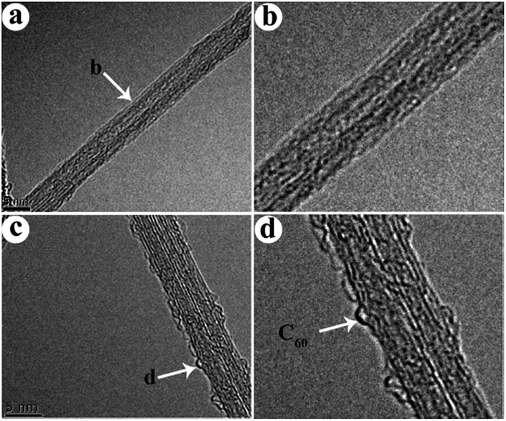 | ||
| Fig. 2 (a) HRTEM image of CNTs after, (b) magnified image of (a), (c) HRTEM image of CNBs, (d) magnified image of (c). | ||
To further corroborate the formation of CNBs structure, Raman spectra of CNBs were carried out, as shown in Fig. 3. The IG/ID ratio is ∼9, indicating low defectiveness of the CNTs. The presence of this D band indicated the CNBs structure. Since even tiny bonded carbon from addition reaction can result in the intensity increase of D band, the covalent bonding of C60 attached to the CNTs surface can account for this increase. It is well known that Raman active modes of C60 are measurable at ambient condition. However, vibrational modes of C60 in CNBs structure are difficult to detect due to the strong intensity of vibrational modes from CNTs. Thus, in this study, based on the previous reports,6c,15 excitation energy of 2.33 eV was applied to detect the vibrational modes of C60 in CNBs structure. Clearly, it is significant to note that C60 fullerenes in the assembled structures showed a red-shift (softening) in their position. As shown in Fig. 3b, the Hg(1) mode of C60 fullerenes is red shifted from 272 cm−1 to 270 cm−1. And the Ag(2) mode (pentagon pinch mode) of C60 fullerenes is red shifted from 1464 cm−1 to 1462 cm−1, shown in Fig. 3c. These red shifts in the C60 modes are indicative of strong interaction between the two types of nano-building blocks within the assembled structure of CNBs. Similar result can also be found in previous report.16 The simultaneous observation of vibrational modes of both C60 and CNTs clearly demonstrates the successful preparation of CNBs, which is consistent with result obtained from HRTEM (Fig. 2).
 | ||
| Fig. 3 (a) Raman spectrum of the CNBs, C60 and CNTs; (b) and (c) magnified Raman spectrum of the CNBs, C60 and CNTs in the range of 100–300 cm−1 and 1300–1800 cm−1, respectively. | ||
A possible mechanism was proposed to explain the formation of CNBs by RF plasma treatment. By treating with RF plasma, N2 can be excited as the active nitrogen species (i.e. N*, shown in Fig. S8†).11a The in situ generated active nitrogen species (i.e. N*) can easily react with CNTs to form large amounts of active active [CNTs]* because of its large surface area. Simultaneously, the active nitrogen species (i.e. N*) can also react with C60 to form [C60]*. Finally, the activated [CNTs]* with active carbons can react with and C60 or [C60]* in liquid medium to form CNBs.17,18 Additionally, the formation mechanism of CNBs is just anticipation, since it has no data to support it, and the precise formation mechanism of CNBs is still under processing. However, as previously reported,7,19,20 C60 in CNBs would likely be damaged by the electron beam considering the limited free available carbon atoms provided by CNTs. To repair the damage of anchored C60 induced by the electron beam, weakly bonded carbon atoms are supposed to move to C60 over the surface of CNTs, during which the carbon atoms are very likely to be trapped due to large coverage of amorphous carbon structures on the outer surface of CNTs. During the RF plasma treatment, the Tp (plasma temperature) is within the range of 2 × 10³ to 3 × 10⁴ K,21 which equals to beam energies of 0.2–3 eV, much lower than the C60 total bond energy (eV) of 419.75 eV.22 Thus, it can be inferred that the C60 cannot be damaged during the RF plasma treatment. The defects caused by the electron beam from the TEM may also lead to the formation of CNBs. As discussed above, the formation of CNBs can be attributed to two aspects, being the cycloaddition between C60 and CNTs and the defects caused by the electrons generated during the TEM characterization. Fig. 4 provided a possible schematic depiction of the formation mechanism of CNBs through the cycloaddition between C60 and CNTs.
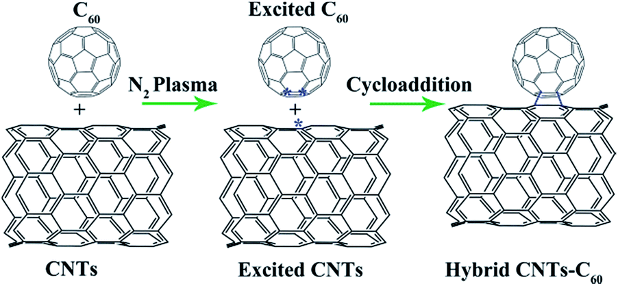 | ||
| Fig. 4 Schematic presentation of the CNBs formation. | ||
In summary, an efficient, economical and easy to operate method was developed for the successful synthesis of CNBs. The CNBs structure was confirmed by HRTEM in combination with Raman spectroscopy. The CNBs structures created here may be utilized as precursors in synthetic processes of nanotube junctions which can be further applied to composite and electronic fields. Additionally, since current CNBs form a relatively small percentage of CNTs, the scale-up of the production of CNBs is under investigation, to demonstrate the robustness of this new technique.
Acknowledgements
We are grateful for financial support from the National Natural Science Foundation of China (21272236, 21677146, U1530131). The Jiangsu Provincial Key Laboratory of Radiation Medicine and Protection and the Priority Academic Program Development of Jiangsu Higher Education Institutions are also acknowledged.Notes and references
- (a) J. I. Choi, H. S. Kim, H. S. Kim, G. I. Lee, J. K. Kang and Y. H. Kim, Nanoscale, 2016, 8, 2343–2349 RSC; (b) A. V. Talyzin, I. V. Anoshkin, A. V. Krasheninnikov, R. M. Nieminen, A. G. Nasibulin, H. Jiang and E. I. Kauppinen, Nano Lett., 2011, 11, 4352–4356 CrossRef CAS PubMed; (c) A. Chuvilin, E. Bichoutskaia, M. C. Gimenez-Lopez, T. W. Chamberlain, G. A. Rance, N. Kuganathan, J. Biskupek, U. Kaiser and A. N. Khlobystov, Nat. Mater., 2011, 10, 687–692 CrossRef CAS PubMed; (d) Y. G. Li, W. Zhou, H. L. Wang, L. M. Xie, Y. Y. Liang, F. Wei, J. C. Idrobo, S. J. Pennycook and H. J. Dai, Nat. Nanotechnol., 2012, 7, 394–400 CrossRef CAS PubMed.
- B. W. Smith, M. Monthioux and D. E. Luzzi, Nature, 1998, 396, 323–324 CrossRef CAS.
- S. B. Chikkannanavar and D. E. Luzzi, Nano Lett., 2005, 5, 151–155 CrossRef CAS PubMed.
- H. J. Shen, Mater. Lett., 2007, 61, 527–530 CrossRef CAS.
- M. Vizuete, M. Barrejón, M. J. Gómez-Escalonilla and F. Langa, Nanoscale, 2012, 4, 4370–4381 RSC.
- (a) A. G. Nasibulin, P. V. Pikhitsa, H. Jiang, D. P. Brown, A. V. Krasheninnikov, A. S. Anisimov, P. Queipo, A. Moisala, D. Gonzalez, G. Lientschnig, A. Hassanien, S. D. Shandakov, G. Lolli, D. E. Resaco, M. Chol, D. Tománek and E. I. Kauppinen, Nat. Nanotechnol., 2007, 2, 156–161 CrossRef CAS PubMed; (b) A. G. Nasibulin, A. S. Anisimov, P. V. Pikhitsa, H. Jiang, D. P. Brown, M. Choi and E. I. Kauppinen, Chem. Phys. Lett., 2007, 446, 109–114 CrossRef CAS; (c) Y. Tian, D. Chassaing, A. G. Nasibulin, P. Ayala, H. Jiang, A. S. Anisimov and E. I. Kauppinen, J. Am. Chem. Soc., 2008, 130, 7188–7189 CrossRef CAS PubMed.
- R. J. Nicholls, J. Britton, S. S. Meysami, A. A. Koós and N. Grobert, Chem. Commun., 2013, 49, 10956–10958 RSC.
- (a) A. Sarmah and R. K. Roy, Chem. Phys., 2016, 472, 218–228 CrossRef CAS; (b) X. Wu and X. C. Zeng, Nano Lett., 2009, 9, 250–256 CrossRef CAS PubMed; (c) H. Y. He and B. C. Pan, J. Phys. Chem. C, 2009, 113, 20822–20826 CrossRef CAS; (d) A. Seif, E. Zahedi and T. S. Ahmadi, Eur. Phys. J. B, 2011, 82, 147–152 CrossRef CAS; (e) J. Raula, M. Makowska, J. Lahtinen, A. Sillanpää, N. Runeberg, J. Tarus, M. Heino, E. T. Seppälä, H. Jiang and E. I. Kauppinen, Chem. Mater., 2010, 22, 4347–4349 CrossRef CAS.
- J. Wang, K. S. Liao, D. Früchtl, Y. Tian, A. Gilchrist, N. J. Alley, E. Andreoli, B. Aitchison, A. G. Nasibulin, H. J. Byrne, E. I. Kauppinen, L. Zhang, W. J. Blau and S. A. Curran, Mater. Chem. Phys., 2012, 133, 992–997 CrossRef CAS.
- B. Akhavan, K. Jarvis and P. Majewski, ACS Appl. Mater. Interfaces, 2015, 7, 4265–4274 CAS.
- (a) D. D. Shao, J. Hu and X. K. Wang, Plasma Processes Polym., 2010, 7, 977–985 CrossRef CAS; (b) D. Shao, J. Hu, C. L. Chen, G. D. Sheng, X. M. Ren and X. K. Wang, J. Phys. Chem. C, 2010, 114, 21524–21530 CrossRef CAS.
- Y. Tian, D. Chassaing, A. G. Nasibulin, P. Ayala, H. Jiang, A. S. Anisimov, A. Hassanien and E. I. Kauppinen, Phys. Status Solidi B, 2008, 245, 2047–2050 CrossRef CAS.
- (a) J. H. Yao, Y. J. Zou, X. W. Zhang and G. H. Chen, Thin Solid Films, 1997, 305, 22–25 CrossRef CAS; (b) S. G. Wang, E. K. Tian and C. W. Lung, J. Phys. Chem. Solids, 2000, 61, 1295–1300 CrossRef CAS; (c) J. Zhang, F. Ma and K. Xu, Appl. Surf. Sci., 2004, 229, 34–42 CrossRef CAS.
- H. S. Shin, S. M. Yoon, Q. Tang, B. Chon, T. Joo and H. C. Choi, Angew. Chem., 2008, 120, 705–708 CrossRef.
- (a) T. Pichler, H. Kuzmany, H. Kataura and Y. Achiba, Phys. Rev. Lett., 2001, 87, 267401 CrossRef CAS PubMed; (b) R. Pfeiffer, H. Kuzmany, W. Plank, T. Pichler, H. Kataura and Y. Achiba, Diamond Relat. Mater., 2002, 11, 957–960 CrossRef CAS; (c) P. M. Rafailov, C. Thomsen and H. Kataura, Phys. Rev. B: Condens. Matter Mater. Phys., 2003, 68, 193411 CrossRef.
- M. S. Amer and J. D. Busbee, J. Phys. Chem. C, 2011, 115, 10483–10488 CAS.
- A. Hirsch, Synthesis, 1995, 895–913 CrossRef CAS.
- (a) M. Ueda, T. Sakaguchi, M. Hayama, T. Nakagawa, Y. Matsuo, A. Munechika, S. Yoshida, H. Yasudad and I. Ryu, Chem. Commun., 2016, 52, 13175–13178 RSC; (b) S. Yano, M. Naemura, A. Toshimitsu, M. Akiyama, A. Ikeda, J. Kikuchi, X. D. Shen, Q. Duan, A. Narumi, M. Inoue, K. Ohkubo and S. Fukuzumi, Chem. Commun., 2015, 51, 16605–16608 RSC.
- T. Füller and F. Banhart, Chem. Phys. Lett., 1996, 254, 372–378 CrossRef.
- F. Ding, Z. Xu, B. I. Yakobson, R. J. Young, I. A. Kinloch, S. Chu, L. Deng, P. Puech and M. Monthioux, Phys. Rev. B: Condens. Matter Mater. Phys., 2010, 82, 041403 CrossRef.
- H. Huang and L. Tang, Energy Convers. Manage., 2007, 48, 1331–1337 CrossRef CAS.
- D. R. Lide, CRC Handbook of Chemistry and Physics, CRC Press, Taylor & Francis, Boca Raton, 86th edn, 2005, pp. 5–42 Search PubMed.
Footnote |
| † Electronic supplementary information (ESI) available. See DOI: 10.1039/c7ra01530e |
| This journal is © The Royal Society of Chemistry 2017 |