
 Open Access Article
 This Open Access Article is licensed under a
 Creative Commons Attribution 3.0 Unported Licence
Rapid, stable and self-powered perovskite detectors via a fast chemical vapor deposition process†
Guoqing Tonga,
Xiangshun Gengb,
Yongqiang Yub,
Linwei Yu *a,
Jun Xua,
Yang Jiang*b,
Yun Shengc,
Yi Shia and
Kunji Chena
*a,
Jun Xua,
Yang Jiang*b,
Yun Shengc,
Yi Shia and
Kunji Chena
aNational Laboratory of Solid State Microstructures, School of Electronics Science and Engineering, Collaborative Innovation Centre of Advanced Microstructures, Nanjing University, Nanjing 210093, China. E-mail: yulinwei@nju.edu.cn
bSchool of Materials Science and Engineering, Hefei University of Technology, Hefei 230009, P. R. China. E-mail: apjiang@hfut.edu.cn
cState Key Lab of Photovoltaic Science and Technology, Trina Solar, Changzhou 213031, P. R. China
First published on 27th March 2017
Abstract
Organometal halide perovskite materials are outstanding candidates not only for solar cells but also for photo-detection. In this work, we develop a well-controlled lower temperature (<120 °C) and fast chemical vapor deposition process (LFCVD) to fabricate photovoltaic detectors with a high speed response (τrise/τfall ∼ 460 ns/940 ns) and a 3 dB-bandwidth above 0.9 MHz, which are the highest among those with a large active area (>0.1 cm2) without external power supply. Remarkably, the perovskite photovoltaic detectors demonstrate an excellent air-exposure stability for more than two months without particular encapsulation. These excellent performances are attributed to a well-controlled expansive gas–solid reaction and formation of perovskite crystallites that collide and pinch off the pinhole leakage paths at the grain boundaries. More importantly, the accumulated strain at the colliding grain boundaries leads to a selective evaporation of MAI during post-growth annealing, and thus passivate the local defects by the remnant PbI2 layer. These results highlight the potential of LFCVD perovskite materials in developing ultra-fast and self-driven photovoltaic detectors with outstanding stability and scalability.
Introduction
Organometal trihalide perovskites (CH3NH3PbX3, where X = Cl, Br, I, or a mix halide) are emerging new hybrid semiconductors that have enabled a series of exciting optoelectronic applications, including high performance photovoltaics (PV),1–4 light-emission,5,6 lasing7,8 and sensing.9–13 Thanks to a strong broad spectral absorption, a long carrier lifetime and a very high carrier mobility (≈10 cm2 V−1 s−1), the power conversion efficiency of the perovskite solar cells has reached a new record of 20.8%,14–16 and 22.1% very recently.17 In parallel, perovskite materials are promising candidates for rapid photodetections, operating in the visible and near infrared (NIR) spectrum range. For example, Hu Xin and Xie Yi et al. first reported a flexible organic-halide photodetector by one-step solution deposition and exhibited excellent flexibility and reasonable sensitivity.9 Yang Yang et al. demonstrated perovskite photodetectors working at low or even zero bias, with a fast response (τrise/τfall ∼ 0.97 μs/1.1 μs), a large dynamic linear response up to 100 dB and a detectivity approaching 1012 Jones.10 Meanwhile, a high gain (nearly 500) perovskite detector has been achieved by Huang's group at a low driving or bias voltage of −1 V.12Seeking a low-cost, scalable and reliable fabrication of the perovskite solar cells has been crucial to establishing large-scale photovoltaic and detector applications.18–20 All solution-based one-step or two-step spin-coating21–24 deposition are convenient strategies, but usually experience a radical reaction that is hard to control over large area. Alternatively, perovskite thin film can be deposited via sequential25,26 or concurrent15,27 thermal evaporations in expensive high vacuum system, where a precise and readily controllable deposition has been achieved. Recently, a vapor-assisted solution process (VASP),28–30 low pressure VASP (LPVASP),19,31 hybrid chemical vapor deposition (HCVD)32,33 and hybrid physical–chemical vapor deposition (HPCVD)34 have been proposed to combine the solution-based fabrication with a low vacuum deposition and obtained a high performance in perovskite solar cells.
In this work, we explore a well-controlled lower temperature and fast chemical vapour deposition (LF-CVD) process within 20 min to prepare high quality compact perovskite films, and employ them in a vertical photodetector structure of FTO/c-TiO2/CH3NH3PbI3/Spiro-OMeTAD/Ag that exhibits very high speed detection with a response time of τrise/τfall ∼ 460 ns/940 ns, a responsivity of 0.55 A W−1 and a 3 dB bandwidth above 0.9 MHz (the highest among those with a reasonable active area >0.1 cm2) without exterior power supply. Remarkably, all these have been achieved with an excellent air-exposure stability for more than two months without particular encapsulation. We propose that the slowly expansive gas–solid reaction/formation of perovskite crystallites at a relatively lower temperature (<120 °C) is the key to pinch off the pinhole leakages at the grain boundary, while the accumulated strain at the colliding grain boundaries causes a selective evaporation of MAI during post-growth annealing and effective passivation of the local recombination centers by the remnant PbI2 layer. These results highlight the potential of LFCVD perovskite materials in developing ultra-fast and self-driven photovoltaic detectors with outstanding stability and scalability.
Experiments
The LFCVD setup and the fabrication procedure are schematically illustrated in the Fig. 1a. First, a PbI2 thin film was spin-coated on transparent FTO/c-TiO2 substrates. Then, the sample was loaded into a high-vacuum tube furnace in zone II, while MAI (CH3NH3I) powder in crucible were placed in the up-stream in zone I. Note that, the temperatures at different zones can be independently controlled, and the base vacuum in the tube is pumped to 10−3 Pa by turbo molecular pump. Upon heating to ∼120 °C in zone I, the MAI powder starts to evaporate,19,32 and carried by 100 SCCM Ar gas to transport over zone II loaded with PbI2 substrates. During the reaction, the temperature of zone II was kept at 100 °C for 20 min. After that, the samples were in-suit annealed in zone II to remove the excess MAI on the surface. Finally, photovoltaic devices (Fig. 1b) were fabricated following the standard procedures as detailed in the Experiments section. | ||
| Fig. 1 (a) Schematic diagram of the configuration of the two-temperature-zones furnace tube and the fabrication procedure of a lower temperature fast chemical vapor deposition process (LFCVD) for synthesizing perovskite (CH3NH3PbI3) films. (b) The multilayer structure of the final perovskite photovoltaic detector. | ||
Results and discussion
The typical SEM images of the perovskite thin films, before and after annealing at 90 °C, 120 °C and 150 °C, are shown in Fig. 2a–d, respectively. As we can see, the as-prepared perovskite thin film features a compact array of faceted grains with a size of 200–300 nm and a full coverage over the FTO/c-TiO2 glass substrate. After annealing at 90 °C for 30 min in air (see Fig. 2b), the perovskite grains become smoother on the surface and slightly larger in grain size. Increasing the annealing temperature to 120 °C, bright spots appear among the perovskite grains, as witnessed in Fig. 2c, which could be assigned to the decomposition of perovskite back into PbI2 crystals at higher temperature annealing.35–37 Annealing at even higher temperature to 150 °C causes significant damage of the integrity of perovskite thin film, as witnessed in the SEM image shown in Fig. 2d, where large holes and huge grains appear from place to place.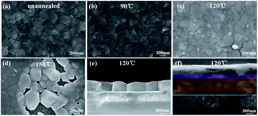 | ||
| Fig. 2 SEM images of the perovskite films deposited via LFCVD procedure on FTO/c-TiO2, (a) before and after annealing at (b) 90 °C, (c) 120 °C and (d) 150 °C for 30 min, respectively. The cross-section SEM image of (e) the perovskite film after annealing at 120 °C for 30 min, (f) the multilayer structure in a complete photovoltaic structure. | ||
The disintegration of perovskite thin film back into PbI2 upon higher temperature post-growth annealing can be inferred from the XRD analysis of the samples plotted in Fig. 3a, where the sharp diffraction peaks found at 12.62° after annealing at 120 °C and 150 °C indicate the formation of PbI2 crystals.19,38 Meanwhile, the absorption spectra of the corresponding samples, as seen in Fig. 3b, show that the annealing temperature ramping causes first an increase of the absorptance after 90 °C or 120 °C, and then drop quickly at high temperature annealing at 150 °C, which can be assigned to the evaporation mass loss and the formation of pinholes in the perovskite thin films.
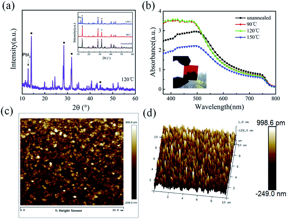 | ||
| Fig. 3 (a) XRD patterns and (b) the absorption spectra of the CH3NH3PbI3 thin films after annealing at different temperature, respectively. (c) 2D, (d) 3D AFM characterizations of the LFCVD CH3NH3PbI3 thin film after annealing at 120 °C on the FTO/c-TiO2 substrate. | ||
Since the density of the PbI2 and CH3NH3PbI3 are 5.85 g cm−3, and 4.17 g cm−3, respectively, a gradual expansion to roughly 40% in volume is expected during the grain formation reaction.28 And this gradual expansion of the perovskite grains is indeed beneficial to fill in or eliminate the voids or vacancy among the perovskite crystals. Meanwhile, we present also atomic force microscopy (AFM) characterizations of the LFCVD perovskite film in Fig. 3c and d, over an area of 10 μm × 10 μm after annealing at 120 °C for 30 min. We found that the surface roughness of the perovskite films is only 23 nm (or <18 nm within 2 μm × 2 μm, see in Fig. S1 (ESI†)). This excellent thin film uniformity, resulting from a gently controlled and slow LFCVD process, is even better than that of previous reports via solution processed films (∼25 nm).39 Note that thin film uniformity is particularly important for improving the junction quality and for preventing the formation of electric leakage path, a prerequisite for high speed and efficient photodetector applications.
Assembled in a complete photovoltaic device, with multilayer structure as indicated in Fig. 2f, the current density and bias voltage (J–V) curves of the perovskite solar cells were measured under AM 1.5 irradiation and presented in Fig. S2 and S3.† The parameters of Voc, Jsc, FF and PCE are extracted and summarized in Table S1.† It is shown that the original sample suffers from a poor contact and large leakage, while post-annealing helps to improve the overall performance substantially, with the highest PCE achieved after annealing at 120 °C, with a high Voc, Jsc, FF and PCE of 1.03 V, 21.25 mA cm−2, 0.69 and 15.1%, respectively. Meanwhile, the Jsc calculated from the solar-spectrum-weighted integral of the corresponding IPCE curve, as seen in Fig. S2,† is 20.2 mA cm−2. However, annealing at higher temperatures leads to a high leakage current and decreased Voc, most likely due to the formation of large pin holes as seen in Fig. 2d. In addition, a hysteresis behaviour is also observed for the LFCVD-processed perovskite thin film photovoltaic device, as witnessed in the forward and backward scan J–V curves presented ESI Fig. S3.†
Serving as a self-driven photodetector, the J–V characteristics of the perovskite photovoltaic device were measured in the dark and under 650 nm light irradiations (with a power density of 1 mW cm−2) and presented in Fig. 4a. A high Jlight/Jdark ratio ∼104 (under −0.1 V bias) has been achieved, under regulated illumination at zero bias (without the need of any external power supply). As an important figure-of-merit for photodetector, the responsivity (R) and the detectivity (D*) of the perovskite devices are extracted according to the formula below,
 | (1) |
 | (2) |
| Ip = aPb ∼ P0.59 | (3) |
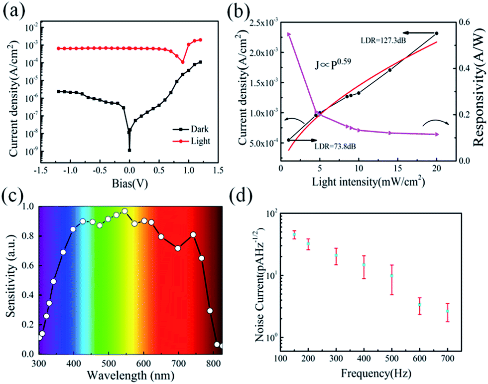 | ||
| Fig. 4 (a) J–V curves of the perovskite photovoltaic device in the dark and under 650 nm irradiation. (b) Linear dynamic range of the perovskite device and the responsivity. (c) Spectral response of the perovskite photodetector. (d) The noise current of the perovskite device measured under dark condition by using a lock-in amplifier (SR830) from 150–700 Hz frequencies at zero bias. | ||
Meanwhile, linear dynamic range (LDR) is another key parameter for photodetector, which is defined as
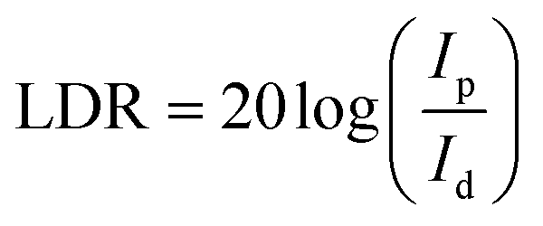 | (4) |
At zero bias, the LDR is estimated to be above 120 dB, which is comparable to the commercial Si photodetector (LDR = 120 dB) and the highest LDR on perovskite photodetectors (LDR = 100 dB).10,40 Note that, this also outperformances most of the 2D nanosheets of transition metal dichalcogenides (TMDs) photodetectors (LDR = 40–80 dB).40 Meanwhile, the noise equivalent power (NEP) of the perovskite photodetector, a measure of the minimum impinging optical power that a device can distinguish from the noise, is defined as
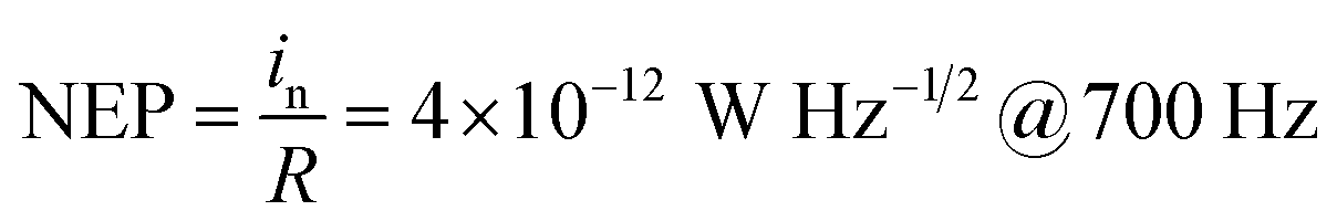 | (5) |
Besides, the characteristic response times of the perovskite photodetectors are also extracted under different modulation frequency ranging from 100 Hz to 4 MHz by a function generator. As shown in Fig. 5a, the perovskite device exhibits an excellent stability and reproducibility at 30 kHz, 300 kHz and 800 kHz modulated light signals, even up to 2.5 MHz (as seen Fig. S4†), which is even higher than that reported in the literature based on nanoribbons (NR) Schottky barrier diodes (500 Hz) and MoS2-based photodetectors (3.3 kHz).41–43 The rise time (τr) and fall time (τf), defined as the rising interval (from 10% to 90% of the maximum) and the falling (from 90% to 10%), are determined to be 460 ns and 940 ns at 300 kHz modulation, respectively. In addition, at 1 MHz, the rise and fall times degrade to 350 ns and 470 ns, but still with a clear waveform output against the noise background, as witnessed in Fig. S4 and S5 (ESI†).
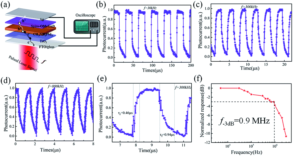 | ||
| Fig. 5 Schematic illustration of the perovskite device to measure photo-response speed. Time response characteristics of the device under different pulsed light illumination (a) perovskite device under pulsed light illumination (650 nm), (b) 30 kHz, (c) 300 kHz, (d) 800 kHz. (e) The magnified and normalized plots of one response cycle 300 kHz. (f) 3 dB bandwidth of perovskite device. | ||
→ Remarkably, we found that the post-annealing also has a very important influence to the photo-response speeds of the perovskite detectors. As seen in Fig. S6 in the ESI† materials, the rise/fall time scales of the original perovskite detector and those annealed at lower (90 °C) or higher (150 °C) temperature, all degrade to 3.7 μs/4.0 μs, 1.1 μs/1.4 μs and 0.8 μs/3.1 μs, respectively, compared to that of 0.46 μs/0.94 μs achieved at optimal annealing at 120 °C. This is because the response time is closely related to the electric quality of the overall perovskite thin film junction. As the perovskite film annealed at 150 °C suffers from a larger current leakage due to the formation of pinholes and voids, the responsive photocurrent signals (that require a build-up progress for an effective read-out in the outer circuit) have to first compensate for this portion of current loss, and thus leading to a slower response. On the other hand, for the original or insufficient annealing at 90 °C, the crystalline quality of the perovskite grains is inferior to that obtained at 120 °C annealing, and thus the photo-carrier transport in the perovskite junction is slower, also limiting the speed of photo-detection. Only the optimized annealing at 120 °C is sufficient and right to improve the grain quality while maintain an integrity of the thin film, as a key basis to achieve a rapid response in photodetection.
In comparison to the other perovskite-based PDs, few-layer MoS2 photodetectors and quantum dot photodetectors, as summarized in Table 110,12,13,44–49 our perovskite photodetectors fabricated with a well-controlled LFCVD process demonstrate the fastest response, thanks to a high quality and compact perovskite thin film formation and the beneficial passivation effect of the remnant PbI2 at the grain boundaries, as will be discussed later. More importantly, as seen in Table 1, our LFCVD-processed perovskite photodetector has achieved an excellent 3 dB bandwidth, the highest one among those with a reasonably large active area (close to 0.1 cm2).10,11 Note that, the bandwidth f3dB is predicted to increase significantly when the area decreases because the 3 dB bandwidth and the response speed are coupled to the resistor–capacitor (RC) constants of the circuitry.
| Device | Preparation process | Active area [cm2] | Rise/fall time [μs] | Bandwidth (f3dB) [MHz] | Ref. |
|---|---|---|---|---|---|
| a Values deduced from time-resolved photoluminescence-lifetime measurements, instead of under direct light signal modulation. | |||||
| FTO/TiO2/perovskite/Spiro-OMeTAD/Ag | LFCVD | 0.1 | 0.46/0.94 | 0.9 | This work |
| ITO/perovskite/TPD-Si/MoO3/Ag | Solution | 0.06 | 5.7/41 | — | 12 |
| FTO/TiO2/Al2O3/PCBM/perovskite/Spiro-OMeTAD/Au/Ag | Solution | 0.07 | 1/3 | — | 13 |
| FTO/TiO2/perovskite/Spiro-OMeTAD/Au | Solution | 0.16 | 17/20 | — | 44 |
| ITO/PEDOT:PSS/perovskite/PC60BM/C60/LiF/Ag | Solution | 0.2 | 1.7/1 | 0.5 | 45 |
| ITO/PEDOT:PSS/perovskite/PCBM/Al | Solution | 0.1 | 0.97/1.1 | 0.8 | 10 |
| 0.01 | 2.9 | ||||
| ITO/PTAA/perovskite/C60/BCP/Cu | Solution | 0.07 | 0.115a | — | 51 |
| ITO/OTPD/perovskite/PCBM/C60/BCP/Al | Solution | 0.07 | 0.28a | 2.9 | 11 |
| Au/perovskite/Au | Solution | — | 300/300 | — | 46 |
| WS2/perovskite heterojunction | Vapor | — | 2.7/7.5 | — | 47 |
| MoS2/Si heterojunction | — | — | 3/40 | — | 48 |
| In/Ga/n-SiNW/CQDs/Au | — | — | 20/40 | — | 49 |
Finally, the stability of perovskite devices has been a critical issue that limits their practical applications. Surprisingly, we found that the photodetectors fabricated via such a mildly-controlled LFCVD exhibited a good stability without encapsulation in the air. As shown in Fig. 6, after a lasting exposure in air (25 °C, RH ∼ 40%) up to 60 days, a clear response to the modulated light signals has been maintained for the perovskite photodetectors. Although the device degrade gradually in terms of rise time, from 0.46 μs to 5.22 μs, particularly pulled down by fall time from 0.94 μs to only 9.04 μs, the response time still faster than most of previous reports, as summarized in Table 1. The deterioration is in general ascribed to the disintegration of Spiro-MeOTAD layer that will happen inevitably in contact with moisture in air.50 Notably, our results provide the first ever experimental proof for the stability issue of the LFCVD-based perovskite photodetectors. One of the reasons could be that this gently controlled vapor deposition and reaction process allows a thorough removal of the residual solvents and thus promotes a high quality crystallization of compact perovskite grains, reducing the metastable phases among the thin films.20,28
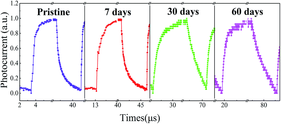 | ||
| Fig. 6 Photo response behaviour of the perovskite device stored in air for 60 days. | ||
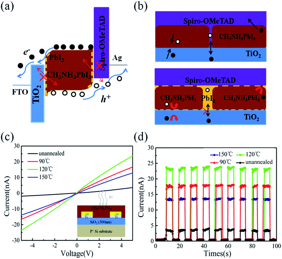
As schematically depicted in Fig. 1b, the LFCVD process allows a milder gas–solid reaction and sufficient time for the MAI vapor to react with the PbI2 crystals, not only on the surface but also deep into the boundary regions among the crystals, which is the key to achieve a uniform and compact perovskite film. This has been supported by the cross-section SEM observation of the LFCVD perovskite thin film after 120 °C annealing presented in Fig. 2e, where all the grain boundary lines are mostly aligned in the normal direction to the substrate, as a result of a strong collision and squeezing among the neighboring expanding grains during the gas–solid reaction. This thus helps to pinch off the pinholes at the grain boundaries, not just on the top surface but all through the thin film down to the root, which is critical to minimize the leakage path of photo-carriers in photovoltaics and photo-detection.
Furthermore, it is important to note that the strain distribution of in the LFCVD perovskite thin film is not uniform, and most of the strain is accumulated at the grain boundaries during the expansion formation of the perovskite grains. As a consequence, during the post-growth annealing, the disintegration and the evaporation of MAI will preferentially happen at the grain boundary regions. This is because, according to the Gibbs-entropy law, if the local pressure is p, the decomposition and evaporation of MAI will become easier and faster as R ∼ eΔE/kT and ΔE = pΩ. Therefore, a thin layer of PbI2 could be left selectively at the grain boundaries, as schematically depicted in Fig. 7. It has been known that, the PbI2 layer has a wider bandgap than perovskite35 and thus provides a good passivation to the boundary of perovskite grains,14,35 which can help to suppress the recombination centres at the boundary, as well the local current leakage along the boundary cracks or voids, as illustrate in Fig. 7b.
 | ||
| Fig. 7 Schematic diagram of (a) band gap of perovskite, PbI2 and perovskite device after passivation, (b) electrons and holes transfer process in the pristine and passivated perovskite film. (c) The current–voltage (I–V) and (d) current–time (I–t) characteristic curves of the perovskite film annealed at different temperatures on the Si substrates under illumination (650 nm, 1 mW cm−2). | ||
This passivation effect can also be inferred from the improved photo-carrier generation and detection in simple planar transport characterizations, where the perovskite thin film is deposited upon SiO2 (300 nm)-coated Si substrates with paired Ti/Au (15 nm/20 nm) electrodes. The channel width and length are 200 μm and 2 μm, respectively as depicted in the inset of Fig. 7c. The I–V curves (under 650 nm illumination, 1 mW cm−2) of the perovskite films treated by different annealing conditions are presented in Fig. 7c, where the linear and symmetric I–V curves imply an ohmic contact between the perovskite thin film and Ti/Au electrodes. Furthermore, Fig. 7d presents time-dependent photoresponse under 5 V bias of the corresponding perovskite thin films, under modulated 650 nm illumination. This observation indicates that the current signals arise indeed from the photo-carriers generated in the perovskite thin film under illumination. Obviously, the highest photo-current response has been achieved for the sample after optimal annealing at 120 °C. This can be attributed to the fact that the residual PbI2 passivation at the grain boundary help to passivate and reduce the recombination centres in the perovskite thin films, and thus a longer photo-carrier lifetime and higher population contribute to a higher photo-current response in the I–V measurement.
Most importantly, as mentioned above, the devices without annealing and annealing at 90 °C and 150 °C show a poor response time estimated to 3.7 μs/4.0 μs, 1.1 μs/1.4 μs and 0.8 μs/3.1 μs, respectively, which is much more slowly than that annealing at 120 °C (0.46 μs/0.94 μs). It indicates that the defect in the film and boundary, to some extent, block the transportation of the exciton and increase the recombination chance, leading to a long response time. These results support that the PbI2 provides a good passivation to the boundary to reduce the recombination centre and effectively increases the photocurrent and improve the response time, leading to a high performance of perovskite photodetector.
Conclusions
In summary, we have demonstrated a well-controlled LFCVD fabrication of high quality perovskite thin film that enables high performance and stable self-sustained photodetector application. The photovoltaic devices under 120 °C annealing for 30 min achieve a PCE as high as 15.1%. Photodetector exhibits a responsivity of 0.55 A W−1, detectivity up to ∼1012 Jones, a fast response (with rise and fall times of 460 ns/940 ns) and a wide 3 dB bandwidth up to 0.9 MHz, with outstanding stability to 60 days air exposure. We propose that the accumulated strain at the colliding grain interfaces leads to a selective formation of PbI2 layer at the grain boundaries that help to passivate local recombination centers and block local current leakage. These benefits combined indicate a new and reliable manufacturing of high performance self-driven photovoltaic and photodetector applications.Acknowledgements
This work was financed by Scientific and Technological Support Programme in Jiangsu province under No. BE2014147-2, NSFC under No. 61674075, 11274155, 61204050, U1632151, Open Research Fund of State Key Laboratory of Pulsed Power Laser Technology of China (Hefei, SKL 2015 KF 04), JSNSFC No. BK20150275, Jiangsu Shuangchuang Team's and Personal Program, Jiangsu Excellent Young Scholar Program and the Fundamental Research Funds for the Central Universities.Notes and references
- Y. Zhao and K. Zhu, Chem. Soc. Rev., 2016, 45, 655–689 RSC.
- O. Malinkiewicz, A. Yella, Y. H. Lee, G. M. Espallargas, M. Graetzel, M. K. Nazeeruddin and H. J. Bolink, Nat. Photonics, 2014, 8, 128–132 CrossRef CAS.
- H. T. Wanyi Nie, R. Asadpour, J.-C. Blancon, A. J. Neukirch, G. Gupta, J. J. Crochet, M. Chhowalla, S. Tretiak, M. A. Alam, H.-L. Wang and A. D. Mohite, Science, 2015, 347, 522–525 CrossRef PubMed.
- B. Li, Y. Li, C. Zheng, D. Gao and W. Huang, RSC Adv., 2016, 6, 38079–38091 RSC.
- O. A. Jaramillo-Quintero, R. S. Sanchez, M. Rincon and I. Mora-Sero, J. Phys. Chem. Lett., 2015, 6, 1883–1890 CrossRef CAS PubMed.
- Z. K. Tan, R. S. Moghaddam, M. L. Lai, P. Docampo, R. Higler, F. Deschler, M. Price, A. Sadhanala, L. M. Pazos, D. Credgington, F. Hanusch, T. Bein, H. J. Snaith and R. H. Friend, Nat. Nanotechnol., 2014, 9, 687–692 CrossRef CAS PubMed.
- Q. Zhang, S. T. Ha, X. Liu, T. C. Sum and Q. Xiong, Nano Lett., 2014, 14, 5995–6001 CrossRef CAS PubMed.
- F. Deschler, M. Price, S. Pathak, L. E. Klintberg, D. D. Jarausch, R. Higler, S. Huttner, T. Leijtens, S. D. Stranks, H. J. Snaith, M. Atature, R. T. Phillips and R. H. Friend, J. Phys. Chem. Lett., 2014, 5, 1421–1426 CrossRef CAS PubMed.
- X. Hu, X. Zhang, L. Liang, J. Bao, S. Li, W. Yang and Y. Xie, Adv. Funct. Mater., 2014, 24, 7373–7380 CrossRef CAS.
- L. Dou, Y. M. Yang, J. You, Z. Hong, W. H. Chang, G. Li and Y. Yang, Nat. Commun., 2014, 5, 5404 CrossRef CAS PubMed.
- Y. Fang and J. Huang, Adv. Mater., 2015, 27, 2804–2810 CrossRef CAS PubMed.
- R. Dong, Y. Fang, J. Chae, J. Dai, Z. Xiao, Q. Dong, Y. Yuan, A. Centrone, X. C. Zeng and J. Huang, Adv. Mater., 2015, 27, 1912–1918 CrossRef CAS PubMed.
- B. R. Sutherland, A. K. Johnston, A. H. Ip, J. Xu, V. Adinolfi, P. Kanjanaboos and E. H. Sargent, ACS Photonics, 2015, 2, 1117–1123 CrossRef CAS.
- D. B. W. Tress, M. I. Dar, P. Gao, J. Luo, C. Renevier, K. Schenk, A. Abate, F. Giordano, J. P. Correa Baena, J. D. Decoppet, S. M. Zakeeruddin, M. K. Nazeeruddin, M. Grätzel and A. Hagfeldt, Sci. Adv., 2016, 2, 1501170 Search PubMed.
- M. Liu, M. B. Johnston and H. J. Snaith, Nature, 2013, 501, 395–398 CrossRef CAS PubMed.
- N. J. Jeon, J. H. Noh, W. S. Yang, Y. C. Kim, S. Ryu, J. Seo and S. I. Seok, Nature, 2015, 517, 476–480 CrossRef CAS PubMed.
- National Renewable Energy Laboratory, Best Research Cell Efficiency, accessed: January, 2016, http://www.nrel.gov/ncpv/images/efficiency_chart.jpg.
- H. S. Duan, H. Zhou, Q. Chen, P. Sun, S. Luo, T. B. Song, B. Bob and Y. Yang, Phys. Chem. Chem. Phys., 2015, 17, 112–116 RSC.
- P. F. Luo, Z. F. Liu, W. Xia, C. C. Yuan, J. G. Cheng and Y. W. Lu, ACS Appl. Mater. Interfaces, 2015, 7, 2708–2714 CAS.
- X. Li, D. Bi, C. Yi, J.-D. Décoppet, J. Luo, S. M. Zakeeruddin, A. Hagfeldt and M. Grätzel, Science, 2016, 353, 58–62 CrossRef CAS PubMed.
- H. Zhou, Q. Chen, G. Li, S. Luo, T.-b. Song, H.-S. Duan, Z. Hong, J. You, Y. Liu and Y. Yang, Science, 2014, 345, 542–546 CrossRef CAS PubMed.
- D. Liu and T. L. Kelly, Nat. Photonics, 2013, 8, 133–138 CrossRef.
- N. J. Jeon, J. H. Noh, Y. C. Kim, W. S. Yang, S. Ryu and S. I. Seok, Nat. Mater., 2014, 13, 897–903 CrossRef CAS PubMed.
- J. Burschka, N. Pellet, S.-J. Moon, R. Humphry-Baker, P. Gao, M. K. Nazeeruddin and M. Grätzel, Nature, 2013, 499, 316–319 CrossRef CAS PubMed.
- A. Ng, Z. Ren, Q. Shen, S. H. Cheung, H. C. Gokkaya, G. Bai, J. Wang, L. Yang, S. K. So, A. B. Djurišić, W. W.-f. Leung, J. Hao, W. K. Chan and C. Surya, J. Mater. Chem. A, 2015, 3, 9223–9231 CAS.
- C. W. Chen, H. W. Kang, S. Y. Hsiao, P. F. Yang, K. M. Chiang and H. W. Lin, Adv. Mater., 2014, 26, 6647–6652 CrossRef CAS PubMed.
- O. Malinkiewicz, A. Yella, Y. H. Lee, G. M. Espallargas, M. Graetzel, M. K. Nazeeruddin and H. J. Bolink, Nat. Photonics, 2013, 8, 128–132 CrossRef.
- Q. Chen, H. Zhou, Z. Hong, S. Luo, H. S. Duan, H. H. Wang, Y. Liu, G. Li and Y. Yang, J. Am. Chem. Soc., 2014, 136, 622–625 CrossRef CAS PubMed.
- C. Liu, J. Fan, X. Zhang, Y. Shen, L. Yang and Y. Mai, ACS Appl. Mater. Interfaces, 2015, 7, 9066–9071 CAS.
- J. Mao, H. Zhang, H. He, H. Lu, F. Xie, D. Zhang, K. S. Wong and W. C. H. Choy, RSC Adv., 2015, 5, 73760–73766 RSC.
- Y. Li, J. K. Cooper, R. Buonsanti, C. Giannini, Y. Liu, F. M. Toma and I. D. Sharp, J. Phys. Chem. Lett., 2015, 6, 493–499 CrossRef CAS PubMed.
- M. R. Leyden, M. V. Lee, S. R. Raga and Y. Qi, J. Mater. Chem. A, 2015, 3, 16097–16103 CAS.
- M. R. Leyden, L. K. Ono, S. R. Raga, Y. Kato, S. Wang and Y. Qi, J. Mater. Chem. A, 2014, 2, 18742–18745 CAS.
- Y. Peng, G. Jing and T. Cui, J. Mater. Chem. A, 2015, 3, 12436–12442 CAS.
- Q. Chen, H. Zhou, T. B. Song, S. Luo, Z. Hong, H. S. Duan, L. Dou, Y. Liu and Y. Yang, Nano Lett., 2014, 14, 4158–4163 CrossRef CAS PubMed.
- G. Rajendra Kumar, A. Dennyson Savariraj, S. N. Karthick, S. Selvam, B. Balamuralitharan, H. J. Kim, K. K. Viswanathan, M. Vijaykumar and K. Prabakar, Phys. Chem. Chem. Phys., 2016, 18, 7284–7292 RSC.
- G. E. Eperon, V. M. Burlakov, P. Docampo, A. Goriely and H. J. Snaith, Adv. Funct. Mater., 2014, 24, 151–157 CrossRef CAS.
- T. Supasai, N. Rujisamphan, K. Ullrich, A. Chemseddine and T. Dittrich, Appl. Phys. Lett., 2013, 103, 183906 CrossRef.
- K. N. Liang, D. B. Mitzi and M. T. Prikas, Chem. Mater., 1998, 10, 403 CrossRef CAS.
- X. Geng, Y. Yu, X. Zhou, C. Wang, K. Xu, Y. Zhang, C. Wu, L. Wang, Y. Jiang and Q. Yang, Nano Res., 2016, 1–11 Search PubMed.
- J. P. Lu, J. Lu, H. Liu, B. Liu, K. X. Chan, J. Lin, W. Chen, K. P. Loh and C. H. Sow, ACS Nano, 2014, 8, 6334–6343 CrossRef CAS PubMed.
- W. Choi, M. Y. Cho, A. Konar, J. H. Lee, G. B. Cha, S. C. Hong, S. Kim, J. Kim, D. Jena, J. Joo and S. Kim, Adv. Mater., 2012, 24, 5832–5836 CrossRef CAS PubMed.
- D. Wu, Y. Jiang, Y. Zhang, Y. Yu, Z. Zhu, X. Lan, F. Li, C. Wu, L. Wang and L. Luo, J. Mater. Chem., 2012, 22, 23272–23276 RSC.
- D. Li, G. Dong, W. Li and L. Wang, Sci. Rep., 2015, 5, 7902 CrossRef CAS PubMed.
- Q. Lin, A. Armin, D. M. Lyons, P. L. Burn and P. Meredith, Adv. Mater., 2015, 27, 2060–2064 CrossRef CAS PubMed.
- H. Deng, X. Yang, D. Dong, B. Li, D. Yang, S. Yuan, K. Qiao, Y. B. Cheng, J. Tang and H. Song, Nano Lett., 2015, 15, 7963–7969 CrossRef CAS PubMed.
- C. Ma, Y. Shi, W. Hu, M. H. Chiu, Z. Liu, A. Bera, F. Li, H. Wang, L. J. Li and T. Wu, Adv. Mater., 2016, 28, 3683–3689 CrossRef CAS PubMed.
- L. Wang, J. Jie, Z. Shao, Q. Zhang, X. Zhang, Y. Wang, Z. Sun and S.-T. Lee, Adv. Funct. Mater., 2015, 25, 2910–2919 CrossRef CAS.
- C. Xie, B. Nie, L. H. Zeng, F. X. Liang, M. Z. Wang, L. B. Luo, M. Feng, Y. Q. Yu, C. Y. Wu, Y. C. Wu and S. H. Yu, ACS Nano, 2014, 8, 4015–4022 CrossRef CAS PubMed.
- L. K. Ono, M. R. Leyden, S. Wang and Y. Qi, J. Mater. Chem. A, 2016, 4, 6693–6713 CAS.
- L. Shen, Y. Fang, D. Wang, Y. Bai, Y. Deng, M. Wang, Y. Lu and J. Huang, Adv. Mater., 2016, 28, 10794–10800 CrossRef CAS PubMed.
Footnote |
| † Electronic supplementary information (ESI) available. See DOI: 10.1039/c7ra01430a |
| This journal is © The Royal Society of Chemistry 2017 |