
 Open Access Article
 This Open Access Article is licensed under a
 Creative Commons Attribution 3.0 Unported Licence
Orientation-dependent piezoresponse and high-performance energy harvesting of lead-free (K,Na)NbO3 nanorod arrays†
Yahua Hea,
Zhao Wang *a,
Xiaokang Hub,
Yaxuan Caia,
Luying Lib,
Yihua Gaob,
Xianghui Zhanga,
Zhongbing Huanga,
Yongming Hua and
Haoshuang Gu*a
*a,
Xiaokang Hub,
Yaxuan Caia,
Luying Lib,
Yihua Gaob,
Xianghui Zhanga,
Zhongbing Huanga,
Yongming Hua and
Haoshuang Gu*a
aHubei Collaborative Innovation Center for Advanced Organic Chemical Materials, Hubei Key Laboratory of Ferro & Piezoelectric Materials and Devices, Faculty of Physics & Electronic Sciences, Hubei University, Wuhan, 430062, P. R. China. E-mail: wangzhao@hubu.edu.cn; guhsh@hubu.edu.cn
bCenter for Nanoscale Characterization and Devices, Wuhan National Laboratory for Optoelectronics, Huazhong University of Science and Technology, Wuhan, 430074, China
First published on 17th March 2017
Abstract
Rapid development of modern electronics promotes the research of high-efficiency self-powered devices and systems. Lead-free perovskite potassium sodium niobate (KNN) with high piezoelectric constant and biocompatibility are regarded as one of the most promising materials for building high-performance nanogenerators. In this work, well-aligned KNN nanorod arrays with [110]-orientation were directly grown on SrTiO3 substrates by a one-step hydrothermal method. The growth of the KNN nanorods could be attributed to the orientation of an initial KNN layer and the release of the compressive stress induced by the SrTiO3 substrate. The piezoelectric constant d33 along the [110] orientation of nanorods is ∼140 pm V−1, which is 2.5 times higher than the d33 measured along the [001]-orientation. Those results agree with the first-principles calculation results, where the spontaneous polarization of the orthorhombic KNN lattice is confirmed to be [110]-oriented. Furthermore, the KNN nanorod arrays exhibit an outstanding energy harvesting performance with the impulsive output voltage of 10 V. A laterally-integrated nanogenerator could also be fabricated by making the KNN nanorods laterally aligned in a PDMS layer. This device shows comparative energy harvesting performance to the nanorod arrays, and exhibits much higher flexibility which allows them to be applied in diversified conditions.
Introduction
In recent years, various multi-functional personal electronics and wearable devices with miniaturized dimensions have been developed.1,2 Unlike conventional bulk devices, these micro-scaled devices require some novel features for electrical power sources, such as refined sizes, higher biocompatibility and longer lifetimes, etc. In the past decade, nanogenerators (NGs) based on piezoelectric low-dimensional nanomaterials have attracted great attention due to their capability for generating high-voltage electrical output by harvesting the mechanical energy from the human body movement, air/water flow and moving vehicles, etc.1–7 The electrical power generated by the NGs can be used either to directly power small microelectronic devices with low power consumption or be collected and stored in super-capacitors for driving other devices.8–11After the first report in 2006, substantial efforts have been made by the researchers to improve the electromechanical conversion performance of piezoelectric NGs.12–17 For instance, by making the ZnO nanowires connect in series on the flexible substrate, the output voltage of the ZnO-based NGs could be considerably enhanced.18 Moreover, the passivation of oxygen vacancy and other kinds of defects in the ZnO nanowires could also improve the device performance.19,20 However, the relatively lower piezoelectric constant of ZnO materials limited their further development and practical application. In comparison, the lead-free perovskite piezoelectric oxides such as (K,Na)NbO3 (KNN) exhibit much higher piezoelectric constant than for ZnO materials, and also prove to be biocompatible for implant devices.21–23 Therefore, it seems that an outstanding piezoelectric energy conversion performance of KNN-based NGs could be expected.
However, the performance of such devices reported in the literatures still needs further improved. For example, although the NGs based on KNN-based nanofibers could generate a voltage output with amplitude up to 1.5 V, this is not high enough to drive many low-power-consumption micro-devices such as a LED.24 That effect might be attributed to a loosened polycrystalline structure, limiting the piezoelectric response of the nanofibers. As is well-known, the piezoelectric constants for piezoelectric single-crystals are always much higher than for poly-crystals. However, NGs consisting of single-crystalline KNN nanorods (NRs) did not perform satisfactorily.25,26 The low piezoelectric response could be due to the short length of the NRs or the non-uniformed nanorod array (NRA) structures, thus limiting the piezoelectric potential generated along the axial direction of the NRs. In addition, a buffered layer with similar lattice structure were always needed for the growth of the KNN NRs in the reported works, leading to complex fabrication procedure and higher cost. Therefore, it is essential to develop a simple and cost-effective fabrication technique for growing high-quality KNN NRAs with prolonged NRs and highly ordered structures, and improve the piezoelectric response of the NGs to promote their practical application.
In this work, KNN NRAs with high aspect ratio and uniform array structure were synthesized on the conductive Nb-doped SrTiO3 (STO) single-crystal substrate by a one-step hydrothermal process. A double-layered structure of the NRAs was found by the TEM characterization. Single-crystalline NRs shows a superior piezoelectric property along the axial, rather than the radial direction, which could be explained by the first-principle calculation results. Both the vertically-integrated and laterally-integrated NGs (VINGs and LINGs) based on the KNN NRs exhibited outstanding energy harvesting performance, with high output voltage up to 10 V.
Experimental details
Synthesis of KNN NRAs
The KNN NRAs were synthesized on Nb: STO substrates by using a surfactant-free hydrothermal process. All reagents used in the hydrothermal experiment are analytic pure and bought from the Sinopharm company, including potassium hydroxide (KOH, >82%), sodium hydroxide (NaOH, >96%), and niobium pentoxide (Nb2O5, >99%). The Nb: STO substrates cut along the (100) face were brought from the Shanghai Daheng Optics and Fine Mechanics Co., Ltd. The detailed fabrication procedure was described as follow: firstly, the pellets of KOH and NaOH with mol-ratio of 74/26 were dissolved by distilled (DI) water in a Teflon-lined autoclave (50 mL in volume) to form an alkaline solution with hydroxide concentrations varying from 6 to 12 M. Then 1 g Nb2O5 was added into the alkaline solution, and stirred for 1 h to obtain the hydrothermal precursor. After that, the pre-cleaned substrate was immersed into the precursor. The substrate was kept 5 cm above the bottom of the autoclave by a Teflon holder and exposed to solution in both surface. After being filled to 80% full by DI water, the autoclave was moved into a stainless container and then sealed. Then the autoclave was kept in 190 °C for 24 h to conduct the hydrothermal reaction. After naturally cooled overnight, the substrate was taken out from the autoclave, washed by DI water and ethanol for several times to eliminate the redundant alkaline, and then dried for 6 h at 60 °C.Characterization and measuring method
The structure of the samples was examined by the X-ray diffraction spectrometer (XRD, Bruker D8A25, CuKα, λ = 1.5406 Å). The morphology, selected-area electron diffraction (SAED) patterns and energy dispersive spectrometer (EDS) were characterized by field-emission scanning electron microscopy (FESEM, JEOL JSM7100F) and high-resolution transmission electron microscopy (HRTEM, JEOL JEM 2010). The surface morphology and piezoelectric property of the NRs were measured by using the scanning probe microscopy (SPM) and piezoresponse force microscopy (PFM, NT-MDT). The energy harvesting performance of the NGs were tested by using the electrometer of Keithley 2400 and 2000.Results and discussion
Hydrothermal growth of the KNN NRAs
Fig. 1 shows the SEM images of the as-synthesized KNN NRAs under different alkalinity of the hydrothermal precursor. The top-view images confirm that the surface of all samples were consisting of well aligned KNN NRs standing on the top of the substrates. In order to observe the detailed morphology of the NRAs, the sample were carefully cut and tilted by a certain degree for the cross-section SEM observation. As shown in Fig. 1(e–h), the NRs synthesized under low alkalinity (6–8 M) exhibit good uniformity on size and space distribution, while the tips of the NRs obtained at 10 M are falling over and hooking with the adjacent ones. Moreover, the sample synthesized at 12 M exhibits non-uniformly distributed tower-like nanostructures. We estimated the average length and aspect ratio of the NRs synthesized at different alkalinity by calculating the data of no less than 20 NRs in each sample. The results are shown in Fig. S1† and indicate that both the length and aspect ratio exhibit similar variation with the increase of alkalinity. Among them, the NRs obtained at 8 M shows the highest length (∼5 μm) and aspect ratio (∼40). However, further increase of the alkalinity led to the decrease on both parameters. That should be attributed to the suppressed orientation-growth of the samples at high alkalinity, which always results in the aggregated growth under hydrothermal condition.27 Furthermore, the low-magnification top-view SEM image shown in Fig. S2† confirms that the NRAs could be large-scale grown on the substrate with uniform structure and distribution under the alkalinity of 8 M. The high-magnification SEM image shown in Fig. S3† clearly show the smooth surface of the single crystal nanorods. Therefore, all piezoelectric measurement and energy harvesting performance testing experiments were conducted on this sample. In addition, the composition (mol ratio between K and Na) of the NRAs obtained at the alkalinity of 8 M were estimated to be ∼1.75, according to the X-ray Photoelectron spectroscopy (XPS) results shown in Fig. S4.†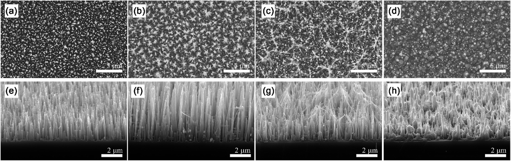 | ||
| Fig. 1 The (a–d) top-view and (e–h) cross-section-view SEM images of KNN NRAs synthesized under different alkalinity. (a and e) 6 M; (b and f) 8 M; (c and g) 10 M; (d and h) 12 M. | ||
For understanding the growth mechanism of the KNN NRAs, the microstructure of the KNN NRs and their interface area with the substrate were studied by the HRTEM characterizations. According to the TEM image and the SAED patterns shown in Fig. 2(a), the KNN NR with ∼100–130 nm in diameter has a single-crystalline orthorhombic structure. Its HRTEM image shown in Fig. 2(b) exhibits clear lattice fringes with the interplanar spacing of 0.401 and 0.393 nm, representing the (110) and (001) faces of the orthorhombic perovskite KNN. These results confirm the [110] growth orientation of the KNN NR. Fig. 2(c) shows the TEM image of the interface area, which exhibits clear edge between the substrate and the as-grown layers. The clearer interface could be found in the HRTEM image shown in Fig. 2(d) with higher contrast difference. According to the Fourier filtered images, the interplanar spacing of the out-plane lattice faces in the upper and lower region were ∼0.389 and 0.382 nm, while those of the in-plane lattice faces were ∼0.280 and 0.274 nm, respectively. The EDS mapping result further confirmed the differences in the interface areas. As shown in Fig. 2(e–i), a continues layer composed of KNN could be found on top of the substrate, which should correspond to the upper layer shown in the HRTEM image (Fig. 2(d)). As a result, the lattice faces with spacing of 0.389 and 0.280 nm could be indexed as the (110) and (1![[1 with combining macron]](https://www.rsc.org/images/entities/char_0031_0304.gif) 1) faces of the orthorhombic KNN lattice. Moreover, the spacing of (110) faces of this initial KNN layer is obviously lower than that of the KNN NRs shown in Fig. 2(b), which should be due to the clamping effect of the small STO lattice during the epitaxial growth process of the initial layer.23 Under the compressive stress induced by the STO substrate, the top of the layer tends to undertake the anisotropic growth to release the stress and forms the one-dimensional nanostructure with slightly larger lattice.
1) faces of the orthorhombic KNN lattice. Moreover, the spacing of (110) faces of this initial KNN layer is obviously lower than that of the KNN NRs shown in Fig. 2(b), which should be due to the clamping effect of the small STO lattice during the epitaxial growth process of the initial layer.23 Under the compressive stress induced by the STO substrate, the top of the layer tends to undertake the anisotropic growth to release the stress and forms the one-dimensional nanostructure with slightly larger lattice.
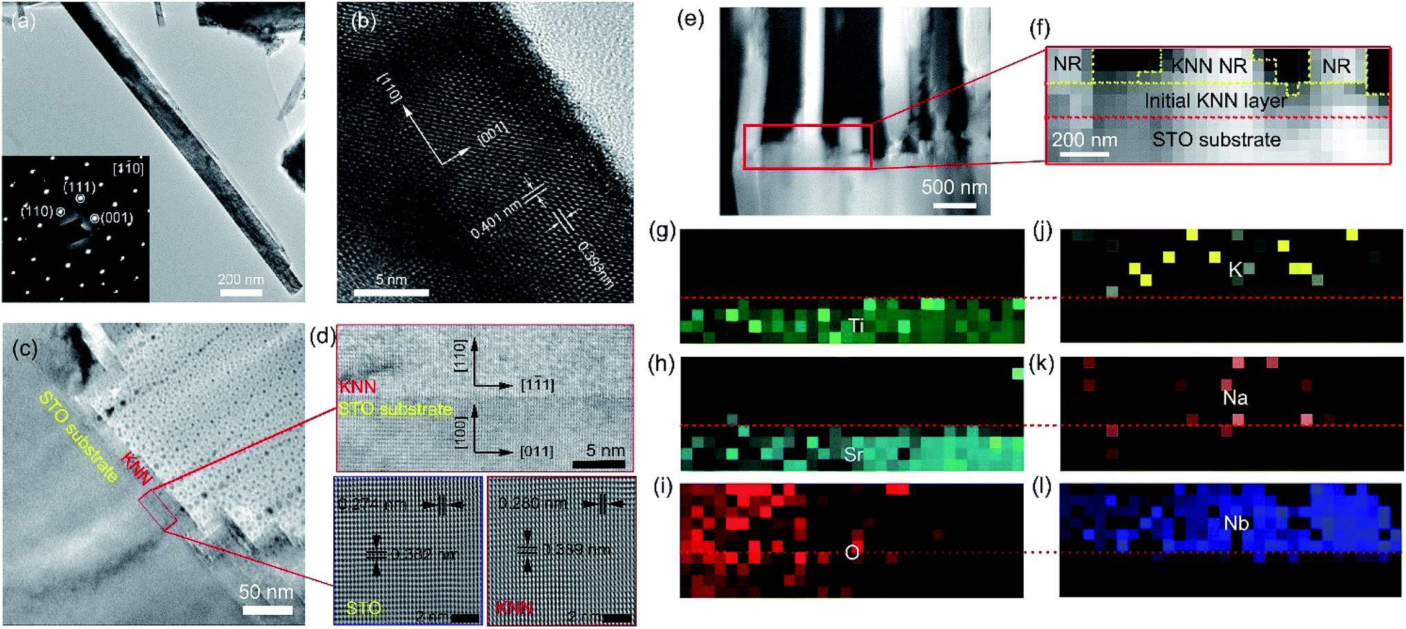 | ||
| Fig. 2 The TEM characterization results of the KNN NRAs obtained at the alkalinity of 8 M. (a) TEM image and SAED patterns of an individual KNN NR. (b) The HRTEM image of the KNN NR. (c) THe local TEM image showing the bottom area of the KNN NRA. (d) The HRTEM and Fourier filtered images obtained from the marked interface area in picture (c). (e–f) The cross-section TEM image of KNN NRA. (g–i) The EDS mapping result of the KNN NRA shwon in picture (f). | ||
The double-layered structure of the KNN NRAs grown on the substrate could also be confirmed by the XRD patterns. As shown in Fig. 3, all diffraction peaks except the sharp STO-related peaks at 22.8° and 46.5° can be indexed to the orthorhombic KNN structure. Among them, the diffraction peaks at 22° and 45° can be attributed to the (110) faces of the KNN NRs (JCPDS card no. 32–0822), while the peaks at 22.4° and 45.7° belongs to the (110) faces of the initial KNN layers with smaller lattices volumes than the NRs. The differences on the interplanar spacing among the 22° (0.401 nm), 22.4° (0.396 nm) and 22.8° (0.390 nm) peaks agrees with the HRTEM results shown in Fig. 2(d). The larger interplanar spacing of the XRD result for 22.4° and 22.8° peaks than the HRTEM results should be due to the measurement error during the TEM characterization process. In addition, the relative intensity between the diffraction peaks of KNN NRAs and initial KNN layer was changed with the alkalinity of the hydrothermal precursors. The sample obtained at 6 M of alkalinity shows the most intensive peak of the initial layer, which should be attributed to the much shorter KNN NRs on the initial layer, leading to stronger interaction between the X-ray and the initial layers. As the alkalinity was increased to 10 M, the diffraction of the NRAs became much stronger than that of the initial layers thanks to the lengthened NRs and weak interaction of X-ray with the initial layer. However, the diffraction peaks of the initial layer were increased due to the decreased NRs' length and aspect ratio, when the alkalinity was increased to 12 M. Those results could further prove the formation of an initial KNN layer with smaller lattice volume on the surface of the STO substrate, which serves as the seed layer for the further growth of KNN NRs to release the compressive stress induced by the clamping effect of the STO substrate.
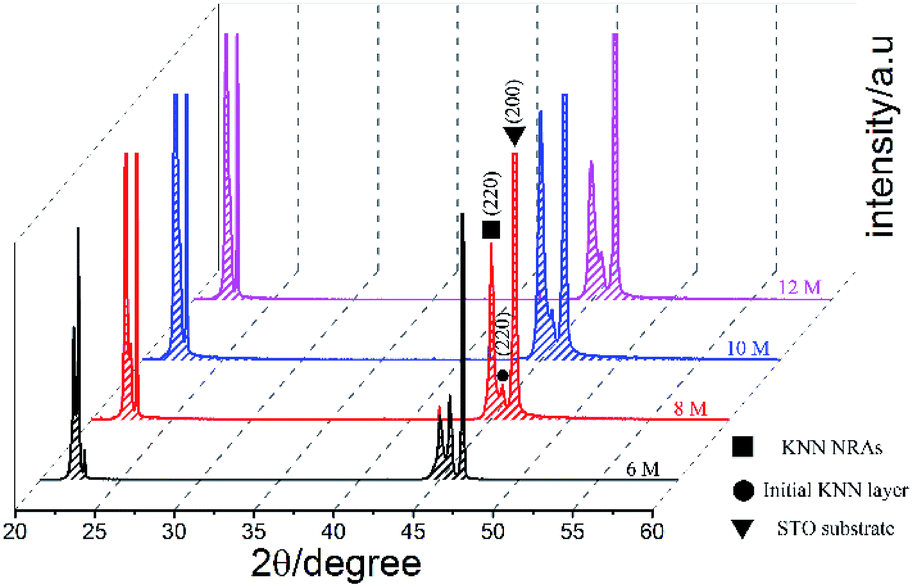 | ||
| Fig. 3 The XRD patterns of KNN NRAs synthesized under different alkalinity. | ||
Piezoelectric response of the NRs
Both the radial and axial piezoelectric response were measured by using the PFM method to evaluate the piezoelectric performance of the KNN NR along different orientation. Firstly, an individual KNN NR was taken from the KNN NRAs and placed on the Au-coated silicon substrate for testing the radial piezoelectric response (along the [001] orientation). Fig. 4(a) shows the surface morphology of the NR, which is ∼1 μm in length and 40 nm in diameter, respectively. The conductive tip was placed on the top surface of the KNN NR, and an external electrical field was added between the tip and substrate. As shown in Fig. 4(b), the NR exhibited obvious butterfly-shape piezoelectric response loop, with maximum deformation of ∼100 pm under a DC bias of 3 V. The phase loop of the piezoelectric response shown in Fig. 4(c) also confirmed the spontaneous polarization behavior of the KNN NR. Fig. 4(d) shows the piezo-response of single nanorod obtained as M = A![[thin space (1/6-em)]](https://www.rsc.org/images/entities/char_2009.gif) cosθ, where M, A and q represent piezo-response, amplitude and phase angle, respectively. According to this curve, the maximum deformation was ∼100 pm with phase switching of 180°. Moreover, the piezoelectric constant could also be estimated from the slope of the linear region of the curve. By measuring the PFM performance on 5 different spots on the NRs, the average piezoelectric constant d33 could be calculated to be ∼40 pm V−1 along the radial direction ([001] orientation).
cosθ, where M, A and q represent piezo-response, amplitude and phase angle, respectively. According to this curve, the maximum deformation was ∼100 pm with phase switching of 180°. Moreover, the piezoelectric constant could also be estimated from the slope of the linear region of the curve. By measuring the PFM performance on 5 different spots on the NRs, the average piezoelectric constant d33 could be calculated to be ∼40 pm V−1 along the radial direction ([001] orientation).
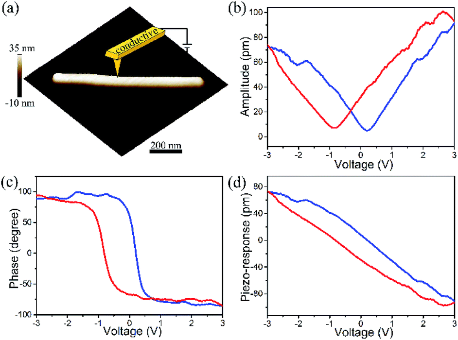 | ||
| Fig. 4 (a) AFM morphology of an individual KNN NR and (b–d) radial PFM characterization results. | ||
Although the KNN NR exhibited obvious piezoelectric response along the radial direction, the piezoelectric energy harvesting performance of the NRs depend more on its axial piezoelectric property. However, the conventional PFM measuring method may lead to the bending or fracturing of the long NRs, when the tip of the AFM probe was landing directly and scanning on the tip of the NRs. And this will largely limit the accuracy of measuring result of the axial piezoelectric response, and may damage the structure of the NRAs. In order to restrict the in-plane motion of the NR during the scanning and landing process, the as-synthesized KNN NRAs were firstly spin-coated with a thin layer of PMMA, leaving the tip of the KNN NRs exposed to the ambient environment for the conducting measurement (shown in Fig. 5(a)). During the PFM testing process, the probe could land on the exposed tip of the NR, and the electrical field could be applied between the top and end of the NR to test the axial piezoelectric response. Fig. 5(b and c) show the SEM and AFM images of the exposed NR tips after the PMMA coating. As shown in Fig. 5(d–f), the NR exhibited obviously superior piezoelectric response along the axial direction rather than the radial direction. The maximum amplitude of the deformation was up to 400 pm under a DC bias of 3 V. The NR also exhibited phase conversion and spontaneous polarization behavior. According to the slope of the curve in Fig. 5(f), the average d33 value of the KNN NR along the axial direction ([110] orientation) was ∼140 pm V−1, which is much higher than the d33 measured along the radial direction ([001] orientation). In addition, all results measured by the PFM methods were calibrated to guarantee the accuracy of the results by using a LiNbO3 single-crystal, which is a commercially available standard sample with a nominal d33 value of 17.3 pm V−1.
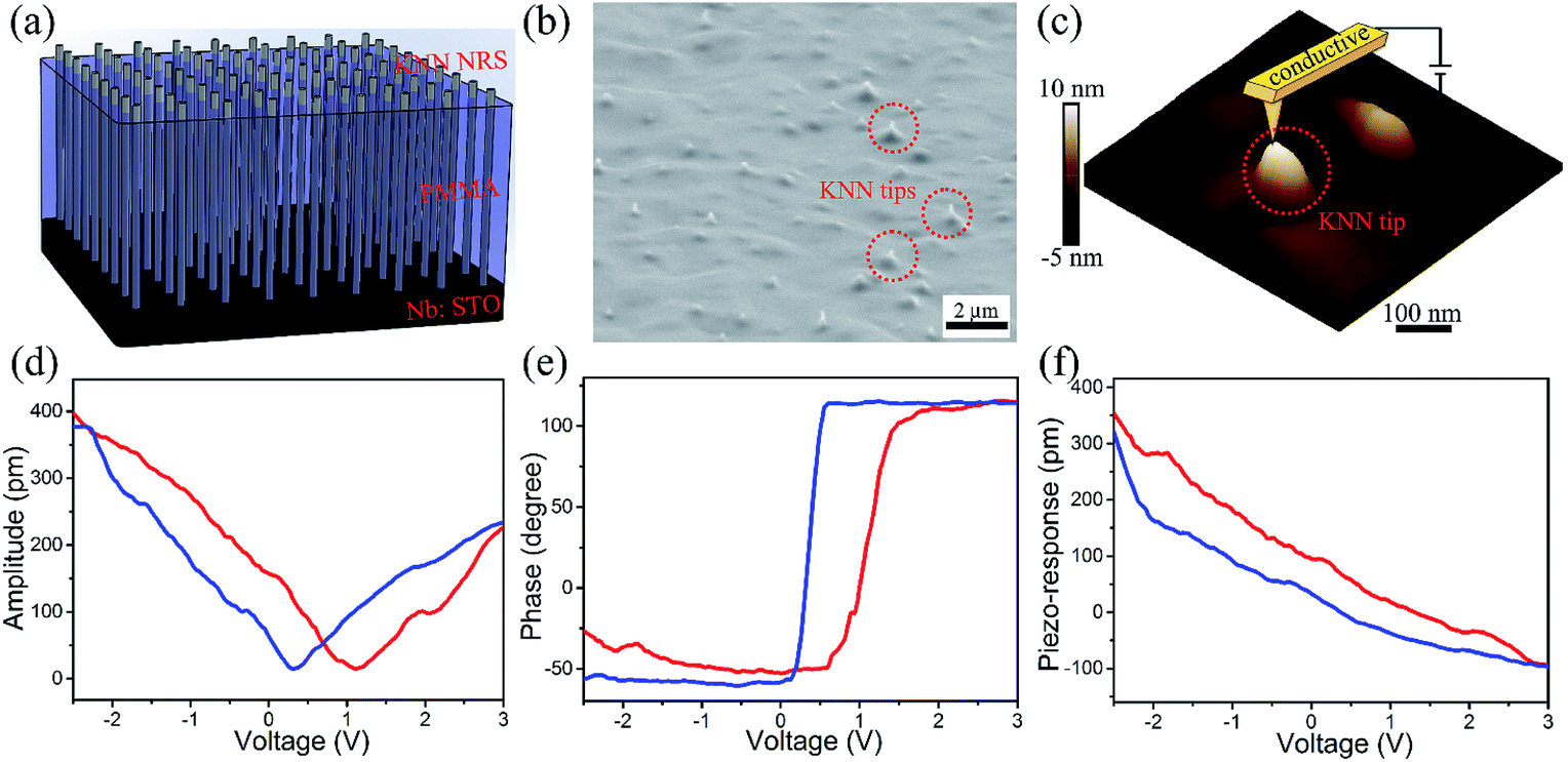 | ||
| Fig. 5 The morphology and axial PFM characterization results of the KNN NR. (a) Schematic diagram of the PFM characterization; (b) surface SEM image (45° tilted) of the PMMA-coated KNN NRAs; (c) AFM image of the PMMA-coated KNN NR array; (d–f) the PFM characterization result along the axial direction of the KNN NR. | ||
In order to explain the orientation-dependent piezoelectric performance of the KNN NRs, a first-principle study on the electronic and ferroelectric properties of the orthorhombic KNN lattice was carried out. The so-called “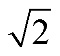 unit cell” is used here to describe the crystal, which is orientated to align the cubic [110] in the x-direction, the [10] in the y-direction and the [001] in the z-direction. As shown in Fig. 6, both the charge density map and deformation charge density map exhibit asymmetric charge distribution along the [110] orientation, which should be due to the displacement of Nb atom from the centre position toward the [110] direction. By using the Berry phase method, the spontaneous polarization was calculated, which has a magnitude of Ps = 38.8569 μC cm−2 along [110] direction, as shown in Table 1. The details of the first-principle calculation were shown in the ESI. Those results could confirm spontaneous polarization of the orthorhombic KNN lattice was along the [110] orientation, which lead to the much higher d33 along this orientation than that along the [001] orientation.21,28
 | ||
| Fig. 6 The lattice structure (a and b), calculated electron density map (c) and deformation density map (d) of orthorhombic KNN by first-principle calculation with contour levels of 0.1 and 0.05 eÅ−3, respectively. | ||
| Lattice parameter (Å) | Polarization (μC cm−2) | ||||
|---|---|---|---|---|---|
| a | b | c | X | Y | Z |
| 5.6950 | 5.7213 | 3.9739 | 38.8569 | −0.0071 | 0.0468 |
Fabrication and performance of the NGs
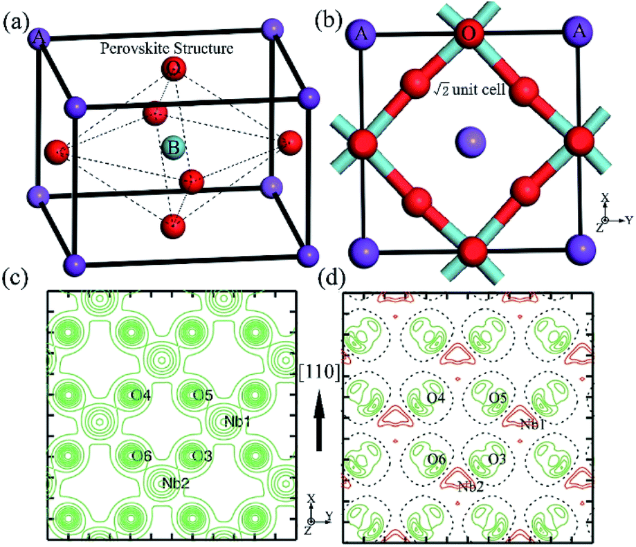
Fig. 7(a–c) show the photo images and schematic diagram of the VINGs based on the PMMA-coated KNN NRAs, which was packaged at the center of a PDMS layer to prevent physical damages and to increase the flexibility of the devices. The device exhibited outstanding energy harvesting behavior when it was vertically pressed by the quick tapping of a human finger. As shown in Fig. 7(d), the VING with KNN NRAs could generate impulsive output voltage with maximum amplitude up to 10 V, which was much higher than the reported value of KNN NRAs in the literatures.22,24–26,29 Meanwhile, the peak value of short-circuit current generated by the VING was ∼50 nA, which is shown in Fig. 7(e). | ||
| Fig. 7 The energy harvesting performance of the as-fabricated VINGs based on KNN NRAs. (a–c) The photo image and schematic diagram of the VINGs; (d and e) the transient output voltage and current generated by the VINGs with/without KNN NRAs when the VINGs were vertically pressed by periodical tapping. (f and g) The transient output voltage and current generated by the VINGs with/without KNN NRAs when the VINGs were bent by a rotating stick. | ||
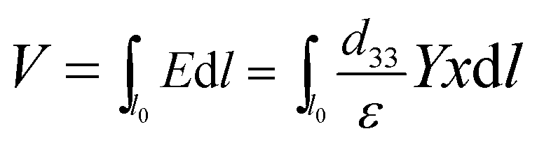
Usually, the impulsive voltage and current generation is attributed to the forward and backward flow of electrons in the external circuit, under the driven force of piezoelectric potential generated by the NRs.30 However, it is worth noting that the thickness variation of the PDMS layers and the dielectric property of the STO substrates may also lead to the release of charges during the pressing process, because the whole system of Au/PDMS/KNN/STO could also be regarded as a dielectric capacitor.31 In order to understand the origin of the energy harvesting behavior of these VINGs, a pair of similar devices were also fabricated, including a bare PDMS polymer with top and bottom electrodes and a Au/PMMA/STO composites. Both devices did not contain any piezoelectric KNN NRAs and were tested by using the same experimental apparatus. The red and blue curve in Fig. 7(d and e) represent the output voltage and current of the bare PDMS sample and Au/PMMA/STO sample, respectively. As shown, no obvious output voltage and current were generated by the bare PDMS sample, while the Au/PMMA/STO sample could generate relatively lower output voltage and current with amplitude of ∼4 V and 20 nA. Moreover, we also measured the dielectric property of the Au/PMMA/STO sample and the VING, of which the relative dielectric constant was calculated to be 300 and 289 at 100 kHZ, respectively. The results suggested the similar dielectric property of both samples, which should be mainly attributed to the much thicker STO substrate than the KNN NRAs. Those results also indicated that both the piezoelectric effect of KNN NRAs and electrostatic effect of STO substrates may contribute to the energy harvesting behavior of the devices. However, the much higher output of the KNN-VINGs than that of the Au/PMMA/STO samples confirmed that the piezoelectric effect should be the predominant contribution of the power generation behavior of the VINGs. In addition, the much higher output voltage of our samples than the reported ones in the literatures could be attributed to the much longer KNN NRs, according to the fundamental piezoelectric voltage equation as
Furthermore, the VING could also be applied as a flexible NG due to the soft PDMS packaging layer, as shown in Fig. 7(c). Consequently, the energy harvesting performance of the device was also tested by using a rotating stick to force the device bent along the in-plane direction. Owing to the NRA structure packaged in the PDMS matrix, the bending of PDMS layer may lead to the bending of the KNN NRs toward the center of the device.32 Fig. 7(f and g) show the transient output voltage and current generated by the VINGs (black), bare PDMS samples (red) and the PDMS packaged Au/PMMA/STO samples (blue). All devices could generate impulsive output voltage during a bending motion. The voltage amplitude of the VINGs (up to 4 V) is similar to that of the Au/PMMA/STO samples, and is approximately twice that of the bare PDMS samples (up to 2 V). The output current exhibits similar tendency. Those results suggested that the energy harvesting behavior of the VINGs under bending mode could mainly be attributed to electrostatic effect rather than the piezoelectric effects. Those results should be due to the restriction of the hard STO substrate and PMMA coating layer to the KNN NRs, which limited their deformation while bending.
In order to improve the flexibility of the KNN-NR based NGs, a flexible LING consisting of laterally integrated KNN NRs in a PDMS matrix were fabricated by the experimental procedure shown in Fig. 8(a). Firstly, the KNN NRs were transferred from the NRAs onto a silicon substrate, by directionally scratching the NRAs with the silicon substrate to make the NRs lying along the same direction. After that, the well-aligned NRs were packaged by a thin layer of PDMS and then lifted off from the silicon substrate to form the KNN–PDMS composite. Then, a pair of Au electrodes were deposited onto the surface of the PDMS layer, which is perpendicular to the to the axial direction of the NRs. Finally, the whole device was packaged by a thick layer of PDMS matrix to prevent physical damage. Fig. 8(b) shows a SEM image of a local area of the KNN–PDMS composite, confirming that most of the transferred NRs were well-aligned on the composite. The alignment of the NRs could optimize the distribution of the piezoelectric electrical field generated by the NRs when they are bent, and thus could result in the integration of piezoelectric potential of all the NRs inside the device, to achieve high energy conversion efficiency.20
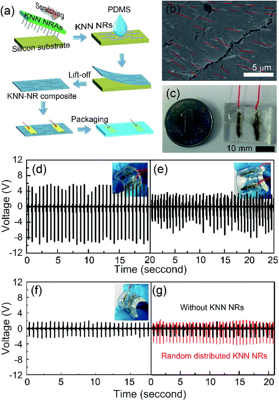 | ||
| Fig. 8 Energy harvesting performance of the as-fabricated LINGs based on the KNN-NR composites. (a) The schematic diagram of the fabrication procedure; (b) a local SEM image of the KNN-NR composite; (c) the photo image of the LING; (d and e) the transient output voltage generated by the LINGs when the top and bottom surface of the device were bent along the axial direction, respectively. (f) The transient output voltage generated by the LINGs when the bottom surface of the device was bent along the radial direction of the NRs; (g) the transient output voltage generated by the LINGs without KNN NRs and with random distributed KNN NRs. | ||
Fig. 8(d–f) shows the transient output voltage generated by the LINGs with different bending state, which is inward-bending and outward-bending along the axial direction, as well as the outward bending along the radial direction of the NRs. Two comparative tests were also conducted by using devices without KNN NRs or with random distributed NRs, which is shown in Fig. 8(g). As shown, both inward and outward bending of the device along the axial direction of the NRs lead to the high voltage generation, with voltage amplitude up to 10 V and 8 V, respectively. The much higher voltage generated by the axial bending, compared to that generated by the devices without KNN NRs, could confirm that the energy harvesting behavior of these devices should mainly be attributed to the piezoelectric effect of the NRs. The lower output voltage generated by the device with random distributed NRs also suggested the importance of nanorod alignment for the energy harvesting performance. Moreover, the relatively lower voltage generated by outward bending could be due to the lower strain of the NRs. During the outward bending process, the soft PDMS polymer at the outside of the device was stretched and became thinner. The tensile stress applied on the KNN NRs will be decreased once the PDMS layer was separated from the NRs. Conversely, the inward bending of the device may apply higher compressive stress on the NRs to make them bend with the PDMS polymer. As a result, higher voltage could be generated by the inward-bending LINGs. In addition, the radial bending of the device cannot lead to the axial bending of well-aligned NRs, and can only result in the deformation of the PDMS layer. Therefore, such motion can only result in the voltage generation lower than 3 V (Fig. 7(f)), which is close to that for devices without KNN NRs, and could be attributed to the release of stored charges between the electrodes.
Moreover, the power generation performance of VINGs and LINGs were both tested as a function of load resistance. Fig. S5 and S6† show output voltage and calculated output power of VINGs with different load resistance, ranging from 10 to 1 GΩ. The output voltages increased with the load resistance, rose sharp after the resistance were increased from 1 MΩ, and reached to the maximum of 1 V at 1 GΩ. Moreover, the maximum output power of the device was ∼2.25 nW at a load resistance of 10 MΩ. The variation of voltage and power should be due to internal resistance of VINGs. Fig. S7 and S8† show output voltage and calculated power of LINGs with different load resistance, both output voltage and power show same tendency as VINGs, the output voltages reach to 0.2 V and then remain the same, the maximum power is about 0.36 nW at 10 MΩ.
Conclusions
In this work, high-quality KNN NRAs with high aspect ratio and uniform distribution were synthesized on the (100)-Nb: STO single crystal substrate by using a large-scalable hydrothermal method. The alkalinity of the hydrothermal precursors plays an important role in the size and morphology of the NRAs. The KNN NRAs were confirmed to be [110]-oriented with the orthorhombic perovskite structure. The growth of KNN NRs can be attributed to the release of compressive stress of an initial KNN layer, which was induced by the clamping effect of the substrate. The NRs exhibited much higher piezoelectric constant d33 along the axial direction than in the radial direction, which is 140 and 40 pm V−1, respectively. The VINGs based on the KNN NRAs could generate impulsive voltage up to 10 V and 4 V when the device was vertically pressed and bent, respectively. The generated power of VINGs could reach to 2.25 nW when load resistance was 10 MΩ. A flexible LING was also fabricated by laterally integrating the KNN NRs on a PDMS matrix. The LINGs exhibited outstanding energy harvesting performance with output voltage and power up to 10 V and 0.36 nW, respectively. This outstanding energy harvesting performance and different device structure of the VINGs and LINGs, based on the as-synthesized KNN NRs, provide great potential of the KNN NGs, and can promote their application as high-performance energy harvesters in diversified conditions.Acknowledgements
This work was financially supported by the National Natural Science Foundation of China (Grant No. 11474088 and 11504099), the Science and Technology Department of Hubei Province (Grant No. 2016AAA002 and 2016CFA081) and Natural Science Project of Hubei Provincial Department of Education (Grant No. Q20141005)Notes and references
- W. Wu, X. Wen and Z. L. Wang, Science, 2013, 340, 952–957 CrossRef CAS PubMed.
- S. Lee, S.-H. Bae, L. Lin, Y. Yang, C. Park, S.-W. Kim, S. N. Cha, H. Kim, Y. J. Park and Z. L. Wang, Adv. Funct. Mater., 2013, 23, 2445–2449 CrossRef CAS.
- R. Zhang, L. Lin, Q. Jing, W. Wu, Y. Zhang, Z. Jiao, L. Yan, R. P. S. Han and Z. L. Wang, Energy Environ. Sci., 2012, 5, 8528 CAS.
- D. A. Wang and H. H. Ko, J. Micromech. Microeng., 2010, 20, 025019 CrossRef.
- Z. Li and Z. L. Wang, Adv. Mater., 2011, 23, 84–89 CrossRef CAS PubMed.
- Z. Wang, X. Pan, Y. He, Y. Hu, H. Gu and Y. Wang, Adv. Mater. Sci. Eng., 2015, 2015, 21 Search PubMed.
- Y. Hu, C. Xu, Y. Zhang, L. Lin, R. L. Snyder and Z. L. Wang, Adv. Mater., 2011, 23, 4068–4071 Search PubMed.
- W. Wenzhuo, Nanotechnology, 2016, 27, 112503 CrossRef PubMed.
- F. Wang, C. Jiang, C. Tang, S. Bi, Q. Wang, D. Du and J. Song, Nano Energy, 2016, 21, 209–216 CrossRef CAS.
- M. Lee, J. Bae, J. Lee, C.-S. Lee, S. Hong and Z. L. Wang, Energy Environ. Sci., 2011, 4, 3359 CAS.
- S. Xu, Y. Qin, C. Xu, Y. Wei, R. Yang and Z. L. Wang, Nat. Nanotechnol., 2010, 5, 366–373 CrossRef CAS PubMed.
- Z. L. Wang, Science, 2006, 312, 242–246 CrossRef CAS PubMed.
- S. K. Karan, R. Bera, S. Paria, A. K. Das, S. Maiti, A. Maitra and B. B. Khatua, Adv. Energy Mater., 2016 DOI:10.1002/aenm.201601016.
- C. Hu, L. Cheng, Z. Wang, Y. Zheng, S. Bai and Y. Qin, Small, 2016, 12, 1315–1321 CrossRef CAS PubMed.
- M. Zhang, T. Gao, J. Wang, J. Liao, Y. Qiu, Q. Yang, H. Xue, Z. Shi, Y. Zhao, Z. Xiong and L. Chen, Nano Energy, 2015, 13, 298–305 CrossRef CAS.
- L. Gu, N. Cui, L. Cheng, Q. Xu, S. Bai, M. Yuan, W. Wu, J. Liu, Y. Zhao, F. Ma, Y. Qin and Z. L. Wang, Nano Lett., 2013, 13, 91–94 CrossRef CAS PubMed.
- X. Chen, S. Xu, N. Yao and Y. Shi, Nano Lett., 2010, 10, 2133–2137 CrossRef CAS PubMed.
- G. Zhu, R. Yang, S. Wang and Z. L. Wang, Nano Lett., 2010, 10, 3151–3155 CrossRef CAS PubMed.
- Y. Hu, L. Lin, Y. Zhang and Z. L. Wang, Adv. Mater., 2012, 24, 110–114 CrossRef CAS PubMed.
- G. Zhu, A. C. Wang, Y. Liu, Y. Zhou and Z. L. Wang, Nano Lett., 2012, 12, 3086–3090 CrossRef CAS PubMed.
- J. Wu, D. Xiao and J. Zhu, Chem. Rev., 2015, 115, 2559–2595 CrossRef CAS PubMed.
- H. B. Kang, J. Chang, K. Koh, L. Lin and Y. S. Cho, ACS Appl. Mater. Interfaces, 2014, 6, 10576–10582 CAS.
- Y. Xu, Q. Yu and J.-F. Li, J. Mater. Chem., 2012, 22, 23221–23226 RSC.
- Z. Wang, Y. Zhang, S. Yang, Y. Hu, S. Wang, H. Gu, Y. Wang, H. L. W. Chan and J. Wang, ACS Appl. Mater. Interfaces, 2015, 7, 4921–4927 CAS.
- P. G. Kang, B. K. Yun, K. D. Sung, T. K. Lee, M. Lee, N. Lee, S. H. Oh, W. Jo, H. J. Seog, C. W. Ahn, I. W. Kim and J. H. Jung, RSC Adv., 2014, 4, 29799–29805 RSC.
- Z. Wang, Y. Hu, W. Wang, D. Zhou, Y. Wang and H. Gu, Integr. Ferroelectr., 2013, 142, 24–30 CrossRef CAS.
- J. He, Y. Hu, Z. Wang, W. Lu, S. Yang, G. Wu, Y. Wang, S. Wang, H. Gu and J. Wang, J. Mater. Chem. C, 2014, 2, 8185–8190 RSC.
- X. Wang, J. Wu, D. Xiao, J. Zhu, X. Cheng, T. Zheng, B. Zhang, X. Lou and X. Wang, J. Am. Chem. Soc., 2014, 136, 2905–2910 CrossRef CAS PubMed.
- J. H. Jung, M. Lee, J.-I. Hong, Y. Ding, C.-Y. Chen, L.-J. Chou and Z. L. Wang, ACS Nano, 2011, 5, 10041–10046 CrossRef CAS PubMed.
- R. Yang, Y. Qin, L. Dai and Z. L. Wang, Nat. Nanotechnol., 2008, 4, 34–39 CrossRef PubMed.
- Z. Su, M. Han, X. Cheng, H. Chen, X. Chen and H. Zhang, Adv. Funct. Mater., 2016, 26, 5524–5533 CrossRef CAS.
- Y. Hu, Y. Zhang, C. Xu, L. Lin, R. L. Snyder and Z. L. Wang, Nano Lett., 2011, 11, 2572–2577 CrossRef CAS PubMed.
Footnote |
| † Electronic supplementary information (ESI) available. See DOI: 10.1039/c7ra01359k |
| This journal is © The Royal Society of Chemistry 2017 |