
 Open Access Article
 This Open Access Article is licensed under a
 Creative Commons Attribution 3.0 Unported Licence
Band gap opening of bilayer graphene by graphene oxide support doping†
Shaobin Tang *a,
Weihua Wua,
Xiaojun Xieb,
Xiaokang Li*a and
Junjing Guc
*a,
Weihua Wua,
Xiaojun Xieb,
Xiaokang Li*a and
Junjing Guc
aKey Laboratory of Organo-Pharmaceutical Chemistry of Jiangxi Province, Gannan Normal University, Ganzhou 341000, China. E-mail: tsb1980@xmu.edu.cn; Fax: +86-797-8393536
bSchool of Physics and Electric Information, Gannan Normal University, Ganzhou 341000, China
cState Key Laboratory of Physical Chemistry of Solid Surfaces, Fujian Provincial Key Laboratory of Theoretical and Computational Chemistry, College of Chemistry and Chemical Engineering, Xiamen University, Xiamen 361005, China
First published on 3rd February 2017
Abstract
The zero-band-gap features of monolayer and bilayer graphene (SLG and BG) limit their applications in logic circuits and photonic devices. Replacing adsorptions of foreign atoms or organic molecules, coupling of BG with derivatives of graphene provides a promising way to modify the electronic properties of BG. In this work, based on first-principles calculations, a sizeable bandgap is created in BG as it is supported on the highly stable graphene oxides (GOs). This result totally differs from the remaining semimetallic behavior of SLG supported on GOs revealed by previous works. The opened band gap can reach values as large as 245–261 meV, which depend on the structure of GOs substrates, including the oxidation species and their atomic arrangement. The effective p-type doping in BG is induced as GO substrates mainly contain the presence of single epoxides. More importantly, the high carrier mobility and large Fermi velocity in supported BG can be maintained due to the weak interaction with GOs. The band gap opening is attributed to the charge transfers between GOs and its neighboring graphene layer, which leads to a significant chemical potential difference between bilayer graphene. Thus, the present work provides a scientific basis for the development of high-performance graphene-based nanodevices.
1. Introduction
Graphene sheets have been the focus of intense research due to their unique structural and electronic properties and potential applications in nanoscale electronics.1–3 Despite the extremely high carrier mobility up to 20![[thin space (1/6-em)]](https://www.rsc.org/images/entities/char_2009.gif) 000 cm2 V−1 s−1, the zero-gap characteristics of pristine graphene has limited its extensive applications in modern electronics.4–7 Several methods have been developed to open the band gap in graphene, including hydrogenation and fluorination,8–11 cutting graphene into ribbons,12–15 the alloying of graphene with hexagonal boron nitride (h-BN),16–18 and graphene–substrate interaction.19–27 However, all these strategies drastically reduce the carrier mobility of graphene or only open a finite band gap due to the destruction of the honeycomb structure and high requirement for the quality of substrate.
000 cm2 V−1 s−1, the zero-gap characteristics of pristine graphene has limited its extensive applications in modern electronics.4–7 Several methods have been developed to open the band gap in graphene, including hydrogenation and fluorination,8–11 cutting graphene into ribbons,12–15 the alloying of graphene with hexagonal boron nitride (h-BN),16–18 and graphene–substrate interaction.19–27 However, all these strategies drastically reduce the carrier mobility of graphene or only open a finite band gap due to the destruction of the honeycomb structure and high requirement for the quality of substrate.
Different from the single layer graphene (SLG), a significant band gap in bilayer graphene (BG) can be induced by applying an external electric field normal to the graphene sheet.28–31 Although the opened band gap in BG can reach 0.25 eV, a large external voltage is required to be applied to both the top and bottoms gates, thus making this approach impractical.31 Charge transfer doping by foreign atoms or organic molecules is another methods affecting the band gap opening and other electronic properties in BG.32–37 In addition, the intercalation effect in BG with various species such as C, B, N, O, and other elements also result in an energy gap opening filled with impurity states.38–42 Unfortunately, some disadvantages induced by these methods are found, such as structural conformation, defects, and clustering of dopants.
The clustering from doping atoms can be avoided by molecular adsorbates due to the repulsion of the charged molecules between each other. More importantly, no defect or strong structural conformation in BG were created after organic molecular adsorption with an electron-donating and/or electro-withdrawing group.43–45 For example, first-principles theoretical calculations43 have revealed that adsorption of tetrafluorotetracyanoquinodimethane (F4-TCNQ) on one side surface of graphene can open the band gap in BG and achieve charge transfers, inducing p-type doping effect. However, chemical doping of BG with organic molecules easily generates highly degenerate semiconducting properties, which moves the Fermi level within the valence band or the conduction band, causing problems in switching device applications.
The stability of organic molecules adsorbed BG systems is very important for the graphene-based nanoelectronic device, because they are mostly environmentally unstable. Very recently, our theoretical works46 reported that replacing the adsorbed organic molecules, the functionalized hexagonal boron nitride (h-BN) substrates with hydrogen and fluorine atoms can lead to n- or p-type doping of graphene, and even open the band gap in graphene. According to this idea, Hu et al.47 proposed a promising way to open a large band gap in BG by sandwiching it between surface functionalized h-BN with H and F atoms. It is reported that BG can have energy gaps ranging from 0.35 eV to 0.55 eV. However, the challenge for such device realization may be comes from the difficult preparation of these functionalized hexagonal boron nitride experimentally. Thus, searching for an effective method for opening band gap in BG still remains challenging.
Graphene oxides (GOs), a derivative of graphene, have emerged as a new class of carbon-based nanoscale materials.48–50 Owing to the presence of the rich oxygen-containing functional groups, combining the GOs with other two-dimensional nanomaterials provides an effective route for fabricating the hybrid structures with novel physical and chemical properties.51,52 Recently, the experiment works combining with DFT calculations53 revealed that after mild O2 plasma treatment on SLG and BG, the sufficiently oxidized SLG shows the semiconducting properties, while the oxidized BLG maintains its semimetallic behavior even at high oxygen level. In addition, by the CH/π or CF/π interaction, other graphene derivatives, such as hydrogenated and fluorinated graphene, is extensively used to couple with graphene for tuning its the electronic properties.54–56
Motivated by these contributions, we investigated the effect of GOs substrates on the electronic properties of bilayer graphene using DFT calculations. The results revealed that in contrast to the metallic properties of SLG/GOs revealed by the experimental reports,53 the BG supported on GOs are semiconductors with sizeable band gap.
2. Computational details
All first-principles calculations were performed within the framework of the plane-wave pseudopotential density-functional theory (DFT) implemented in CASTEP code.57 The Perdew–Burke–Ernzerhof (PBE)58 functional including the van der Waals (vdW) correction proposed by Grimme59 (referred as PBE + D, where D stands for dispersion) was adopted. The ultrasoft pseudopotentials60 for the ion–electron interactions and a kinetic energy cutoff of 350 eV in the plane-wave expansion were used. The two-dimensional (2D) periodic boundary conditions are considered along the growth directions of graphene layer. A vacuum layer of 10 Å is set in the z-direction to avoid the interaction between the periodic images. The 2D Brillouin zone was sampled by 7 × 7 × 1 k-points within the Monkhorst–Pack scheme. In geometry optimization, the whole configuration was allowed to relax until all of the force components on any atom were less than 0.01 eV Å−1. The convergence criterion for energy was chosed as 10−5 eV. Test calculations (see Table S1 in ESI†) showed that increasing the sampling space has less impact on the charge transfers between GOs and BG.In the computational model, we apply supercell of 2 × 2 graphene unit cells consisting of 8 carbon atoms to simulate deposition of BG on GOs substrate. The optimized lattice constant of graphene is 2.46 Å, and the distance between two adjacent graphene layers is evaluated to be 3.35 Å, in excellent agreement with experimental values. The A–B stacking BG is mainly considered due to its higher stability than other patterns.
The atomic structures of GOs have been extensively investigated by experimental and theoretical works.61–76 It is commonly accepted that the oxygen functional groups on the graphene basal plane exist in the form of the hydroxyl and epoxy groups. Some other oxygen functional groups are found, such as five- and six-membered ring lactols.71 More importantly, the recent X-ray photoelectron spectroscopy (XPS) measurements53 showed that after O2 plasma treatment, the epoxy and hydroxyl groups are mainly introduced on the basal plane of oxidated BG. Based on the theoretical calculations, various atomic configurations of GOs including disordered and ordered models were proposed. It is found that epoxy and hydroxyl groups tend to aggregate on graphene plane.66,72 In particular, the band gaps of GOs are well tuned in wide energy range by controlling the oxygen concentration and the atomic arrangement of oxygen groups.66,72,74,76
In our models, therefore, GOs support includes adsorption of the hydroxyl and epoxy groups. We mostly used the model structures of graphite oxide proposed by previous DFT results75 and by XPS measurements53 to simulate GOs support of BG, which are energetically favorable and close to the experimental datas. In these models, the oxidation level and atomic arrangement of the oxygen groups as well as combination of the hydroxyl and epoxy groups were considered. The lattice constant of BG/GOs nanocomposite is set to that of pristine BG. We used BG/GO-mO-nOH-i to represent the hybrid structure between BG and different GOs, in which the m and n define the number of the epoxy and hydroxy groups, respectively, and i marks the atomic configuration of GOs with the same oxygen groups.
To evaluate the stability of hybrid structure between BG and GOs support, the adsorption energies are calculated by: Ea = EBG + EGOs − EBG/GOs, where EBG, EGOs, and EBG/GOs are the total energies of graphene bilayer, GOs, and the hybrid BG/GOs structure, respectively.
3. Results and discussion
3.1. Structures and stabilities of BG/GOs
The semiconducting property of GOs and its high stability make this materials a good candidate for BG support. The considered GOs substrates contain single the epoxy and hydroxyl groups and both them. When several oxygen functional groups are adsorbed on GOs surface, the effect of atomic arrangements of these groups are considered. Fig. 1 shows the adsorption configurations of BG/GOs. Table 1 presents the corresponding adsorption energies and distance between support and BG.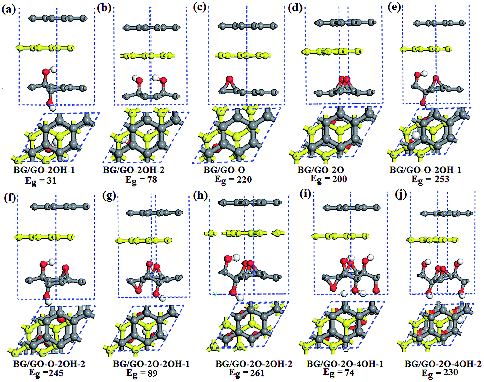 | ||
| Fig. 1 Side and top view of optimized structures of BG/GOs and the corresponding band gap Eg (in meV). The yellow balls represent the bottom graphene layer. | ||
 ) and hole (
 ) effective mass of BG/GOs to pristine BG (the effective mass of isolated BG is evaluated to be m = 0.03me)a
| Structure | Ea | d1 | d2 | Eg | Δq* |
|
|
|---|---|---|---|---|---|---|---|
| a Total positive and negative charges of carbon atoms. | |||||||
| BG/GO-2OH-1 | −26 | 2.47 | 3.37 | 31 | −0.04/0.03 | 1.05 | 1.04 |
| BG/GO-2OH-2 | −32 | 2.62 | 3.3 | 78 | −0.03/0.03 | 1.09 | 1.3 |
| BG/GO-O | −31 | 2.68 | 3.31 | 220 | −0.04/0.0 | 2.18 | 2.07 |
| BG/GO-2O | −32 | 3.08 | 3.14 | 200 | −0.02/0.0 | 2.87 | 1.58 |
| BG/GO-O-2OH-1 | −31 | 3.12 | 3.33 | 253 | −0.03/0.0 | 1.68 | 1.15 |
| BG/GO-O-2OH-2 | −29 | 2.78 | 3.38 | 245 | −0.02/0.02 | 2.96 | 1.46 |
| BG/GO-2O-2OH-1 | −33 | 2.53 | 3.3 | 89 | −0.03/0.02 | 1.13 | 1.24 |
| BG/GO-2O-2OH-2 | −44 | 2.62 | 3.32 | 261 | −0.02/0.0 | 1.56 | 1.31 |
| BG/GO-2O-4OH-1 | −41 | 2.53 | 3.31 | 74 | −0.02/0.04 | 1.13 | 1.18 |
| BG/GO-2O-4OH-2 | −39 | 2.77 | 3.38 | 230 | 0.0/0.02 | 1.71 | 1.11 |

According to different initial position of oxygen groups on substrate relative to bottom graphene layer, we also investigated other stacking patterns of BG/GOs as shown in Fig. S1 in the ESI.† For example, in the case of GO-2O support, the two epoxy groups include three possible configurations with respect to the bottom graphene layer: two oxygen atoms are almost placed beneath the carbon atoms (Fig. 1d), directly below the bridge site of C–C bond (Fig. S1a†), and below the hollow site (Fig. S1b†). Similarly, for the GO-2OH-2, one oxygen from OH points to the carbon atom and the second oxygen to the hollow site (Fig. 1b and S1c†), or the two oxygen are directly below the carbon atoms (Fig. S1d†). The atomic configurations for other stacking are shown in Fig. S1e–h.†
Table S2 in the ESI† presents the corresponding adsorption energy and distance for other BG/GOs structures. Comparing with Tables 1 and S2,† it is found that the stacking configuration of BG/GOs from Fig. 1, whose epoxides and/or H atom from the hydroxyl group are close to the hollow site of neighboring graphene layer, is the ground state among all considered stacking patterns due to the less repulsion or has similar adsorption energy with other patterns, and the largest energy difference between all stacking order for each substrate is less than 7 meV per carbon atom. Thus, we mainly focused on the BG/GOs systems with the ground state in the following.
After geometry relaxation, the distance between BG has no distinct change before and after GOs interaction except for the BG/GO-2O structure. The BG remain the character of basal plane, without breaking the geometric structure of pristine graphene sheet (see Fig. 1). As seen in Table 1, the interlayer spacing between GOs and the bottom graphene layer is in the range of 2.47–3.08 Å, depending on the structure of substrates, which are smaller than that of organic moleculars adsorbed BG.43,44 The sp2 to sp3 hybridization change of carbon networks of GOs and the atomic arrangement of adsorbed oxygen group determine the interlayer spacing. In generally, as shown in Fig. 1e–j, in the presence of both epoxy and hydroxyl groups, the H atom from the hydroxyl group of GOs is more close to the graphene layer than the epoxide. The small distance between GOs and graphene layer plays important role in the charge transfer between them. The Mulliken population analysis (see Table 1) show that there are significant charge transfers from GOs to bottom graphene layer.
Total energy calculations show that the adsorptions of BG on all GOs substrates are energetically favorable with adsorption energies of −208 to −328 meV (corresponding to −26 to −44 meV per carbon atom of graphene layer). Obviously, the coupling of BG with GOs is sensitive to the substrate structures, including the atomic arrangement of oxygen groups as well as oxidation species (see Table 1). The interlayer coupling strength of BG/GOs is comparable to the adsorption of graphene on functionalized h-BN with fluorine and/or hydrogen revealed by the recent reports.46,47 Therefore, the larger interlayer spacing and small adsorption energy indicate the dominant weak interaction between BG and GOs.
3.2. Electronic structures of BG/GOs
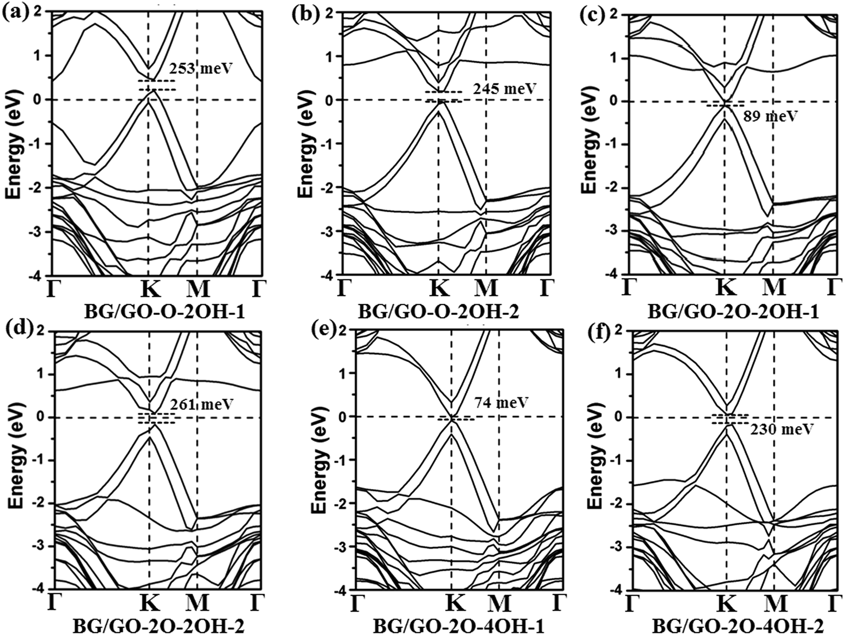
In the following, we investigated the effect of GOs support on the electronic properties of BG. Fig. 2 and 3 present the band structures of BG/GOs. Table 1 also gives the corresponding band gap in BG. When GOs substrates mainly include the hydroxyl groups, the opened band gap in BG is small with 31 meV for GO-2OH-1 (Fig. 2a) and 79 meV for GO-2OH-2 (Fig. 2b). The other stacking orders for BG/GO-2OH-2 also remain the small band gap (see Fig. S2a and b†). However, when BG is supported on GOs with single epoxy group, the band gaps in BG are increased to 200 meV for GO-2O (Fig. 2d) and 220 meV for GO-O (Fig. 2c). Furthermore, the band structures show that the mainly linear energy dispersion of the pristine graphene around K point is preserved. The semiconducting BG/GOs are totally different from O2 plasma-treated BG by previous works,53 in which oxidized BG are metallic.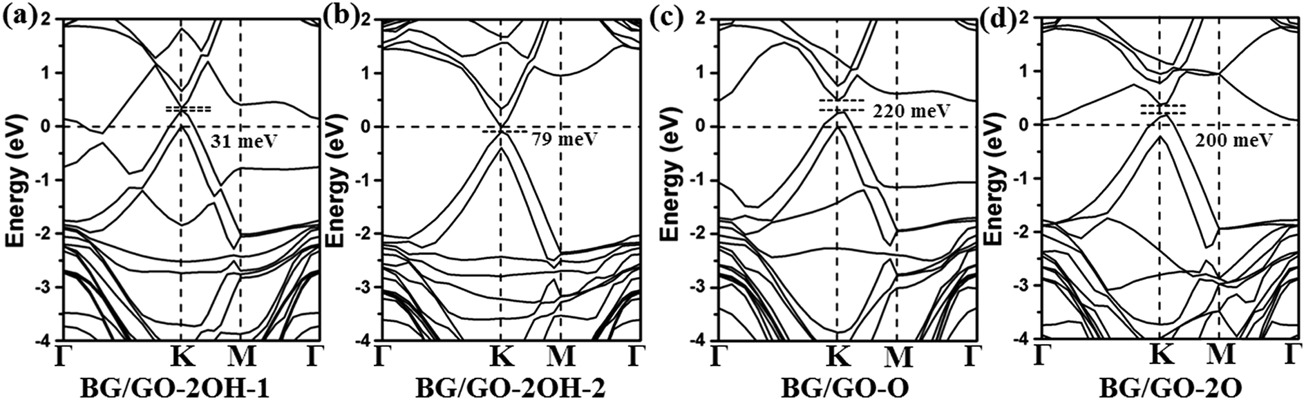 | ||
| Fig. 2 Band structures of BG/GOs only containing single hydroxyl and epoxy groups. The Fermi level is set to 0. The corresponding geometry structures are shown in Fig. 1a–d. | ||
 | ||
| Fig. 3 Band structures of BG/GOs containing both the hydroxyl and epoxy groups. The Fermi level is set to 0. The corresponding geometry structures are shown in Fig. 1e–j. | ||
From Fig. 2c and d, one can clearly find that the Fermi level of BG/GOs nanocomposite is shifted downward, lower than the valence band maximum, indicating the p-type doping of BG. Such doping is also confirmed by the charge transfer from GOs to bottom graphene layer (−0.04 e for GO-O and −0.02 e for GO-2O shown in Table 1). This can be understood by the higher electronegativity of oxygen than the carbon atom of bottom graphene layer. Such the hole doping and band gap opening are also occurred on other systems for interaction of graphene with electron-withdrawing organic groups44,45 or B-doped graphene.35 The band gap value and p-type doping effect in BG induced by GO-2O are independent of the stacking patterns (see Fig. S2c and d†). We also considered other atomic arrangement of two adsorbed epoxides on substrate (see Fig. S3†), the large band gaps are still obtained, while the doped gap states by GOs are found.
As shown in Fig. 3, the coexistence of the epoxide and hydroxyl groups on GOs support can further increases the band gap in BG to 245–261 meV. More importantly, the band structures of these BG/GOs around the Fermi level are very similar to that of pristine BG, indicating no breaking the intrinsic electronic properties of graphene. It is also noticeable that the band gap strongly depends on the atomic arrangement of these oxygen groups on substrate. For example, the band gap of BG supported on GO-2O-2OH-2 or GO-2O-4OH-2 is 261 (Fig. 3d) and 230 meV (Fig. 3f), respectively, whereas this value is lower as the corresponding GOs structure is transformed into other one (89 meV for GO-2O-2OH-1 shown in Fig. 3c and 74 meV GO-2O-4OH-1 in Fig. 3e).
In addition, in the presence of both the epoxide and hydroxyl groups on support, the similar band gap values in BG are found for the other stacking pattern (see Fig. S4†), implying that these systems should be robust and suitable for the real applications. This results are totally different from those previously reported for the BN/BLG/BN system, in which the electronic properties are sensitive to the stacking order.77 The semiconducting BG/GOs are further confirmed by the total density of states (DOS) (see Fig. 4). The projected DOS (PDOS) of BG also suggest that the interaction of GOs substrates not only induces a band gap in BG, and but also maintains the intrinsic electronic properties of pristine graphene. Thus, irrespective of the oxygen density in the GOs substrates, the supported BG is always semiconductor.
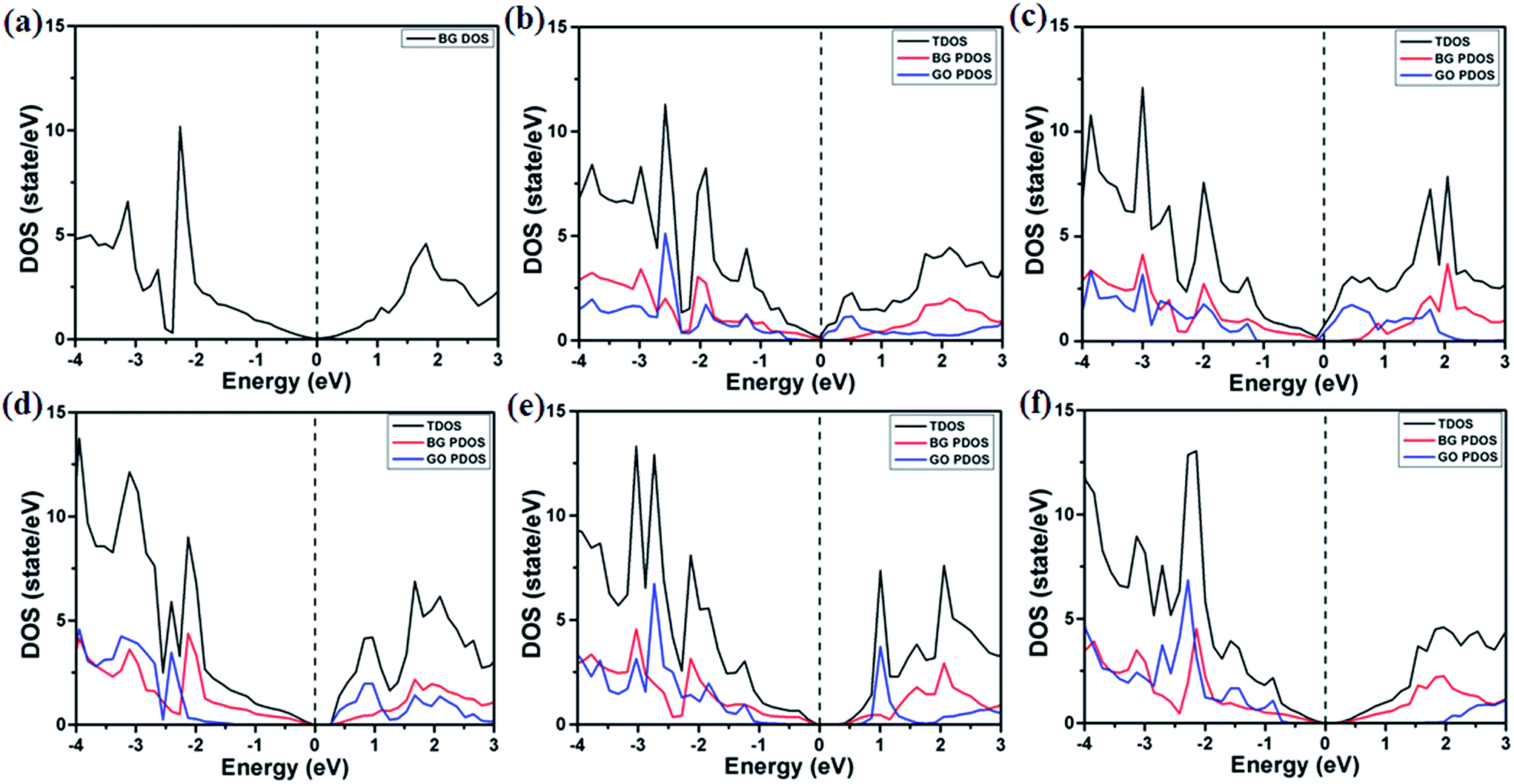 | ||
| Fig. 4 Total density of states (TDOS) of BG/GOs and projected DOS (PDOS) of BG and GOs: (a) pristine BG, (b) BG/GO-O, (c) BG/GO-2O, (d) BG/GO-O-2OH-2, (e) BG/GO-2O-2OH-2, and (f) BG/GO-2O-4OH-2. The Fermi level is set to 0. | ||
The effect of oxidation species of substrates on the electronic properties of BG has a significant difference. Different from only the single epoxides, adsorptions of both the epoxide and hydroxyl groups on substrates lead to less or no doping effect in BG except for GO-O-2OH-1 (see Fig. 3 and S4†). This results may be due to the formation of electron–hole separated domain in bottom graphene layer, in which some carbon atoms have positive charges transferred from GOs and some other carbon have negative charges. In contrast, the GO-O-2OH-1 support leads to the significant net charge transfer because no or less negative charges are transferred from the H atom to carbon atom of graphene due to the larger distance between GO and bottom layer (3.1 Å), compared to other supports (see Table 1). From the PDOS of BG, the downshift of the Fermi level relative to pristine BG suggest the p-type doping by GOs substrate only for adsorption of single epoxy group (see Fig. 4a–c), whereas less doping of BG is found as the GOs contain both the epoxide and hydroxyl groups (Fig. 4d–f).
For the current practical applications of graphene-related nanoelectronics, higher carrier mobility and linear band dispersion are two very important aspects. Thus, we calculated the electron ( ) and hole (
 ) effective mass of the conduction band minimum (CBM) and valence band maximum (VBM) of BG/GOs by
 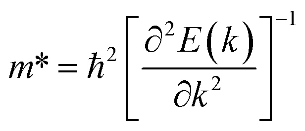 , respectively, where ℏ is the reduced Planck constant, k is the wave vector, and E(k) is the energy dispersion relation with respect to the wave vector k. As shown in Table 1, no remarkable increase of effective mass of charge carrier of BG is found after band gap opening. The calculated
  (or
(or  ) of BG for BG/GOs nanocomposites with large band gap are only 1.11–2.07 (1.65–2.8) times larger than that of freestanding BG. This indicates that in addition to opening a sizeable band gap, the BG of BG/GOs may maintain the high carrier mobility, which provide a potential application in high speed electric devices.
We calculated the carrier mobility (μ) of selected BG/GOs systems using the deformation potential (DP) theory proposed by Bardeen and Shockley.78 Such method is extensively used to predict the carrier mobility of 2D materials, such as Si-based pentagonal monolayer.79 Based on the effective mass approximation, the mobility can be estimated as follows: 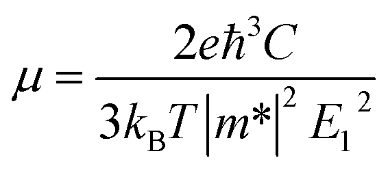 , where e is the electron charge, m* is the carrier effective mass, E1 is defined as ΔE = E1(Δl/l0), in which ΔE is the energy shift of band edge with respect to lattice dilation Δl/l0, and
  is the elastic modulus of the 2D system activated by the applied strain δ, where E is the total energy and S0 is the area of the system. As shown in Table 2, the predicted acoustic-phonon-limited carrier mobility for electron is 0.19–0.29 × 105 cm2 V−1 s−1, while the hole mobility can reach 2.38 × 105 cm2 V−1 s −1. The small deformational potential and small effective mass for GO-O-2OH-2 support are the main reason for high carrier mobility.
| GOs | Carrier type | E1 (eV) | C (N m−1) | m* (me) | μ (×105 cm2 V−1 s−1) |
|---|---|---|---|---|---|
| GO-O-2OH-2 | Electron | 5.38 | 471.27 | 0.089 | 0.29 |
| GO-O-2OH-2 | Hole | 3.8 | 471.27 | 0.044 | 2.38 |
| GO-2O-2OH-2 | Electron | 10.7 | 341.06 | 0.0468 | 0.19 |
| GO-2O-2OH-2 | Hole | 7.38 | 341.06 | 0.0395 | 0.56 |
To further examine the carrier mobility near the Dirac cone, we evaluate the Fermi velocity. Using the π-electron tight-binding approximation, the effective mass of carriers of BG/GOs near the Dirac point can be calculated as m* ≈ Eg/2υF2. Clearly, the Fermi velocity υF is larger with m* smaller, which means higher carrier mobility with appropriate band gap Eg on the BG/GOs nanocomposites. Table 3 presents the Fermi velocity of carrier of VBM and CBM of BG/GOs with larger band gap. The calculated results show that the Fermi velocity of BG remains large values of 5.1–8.0 × 10⁵ m s−1, which has the same order of monolayer graphene (9.5 × 10⁵ m s−1).80 Previous experimental reports48 also revealed that the Fermi velocity in epoxidized BG prepared by O2 plasma treatment is remarkably comparable with that of pristine monolayer graphene.
| υF | BG/GO-O | BG/GO-O-2OH-1 | BG/GO-2O-2OH-2 | BG/GO-2O-4OH-2 |
|---|---|---|---|---|
| Electron | 5.57 × 10⁵ | 6.6 × 10⁵ | 6.8 × 10⁵ | 6.3 × 10⁵ |
| Hole | 5.4 × 10⁵ | 8.0 × 10⁵ | 8.0 × 10⁵ | 7.8 × 10⁵ |
The GOs models contain the high oxygen concentration larger than 0.25 as discussion above, which may present some restriction in wide applications of graphene-based nanoelectronics. To reduce the oxidation level of graphene, we also used supercell of 4 × 4 graphene consisting of 32 carbon atoms to simulate BG/GOs nanocomposites. Only three GOs supports are considered: adsorption of one epoxide, two epoxides, and two epoxides and two hydroxyl groups, which correspond to 0.062, 0.125, and 0.187 oxygen concentration, respectively. Fig. S5a–f† present the geometry structures and the corresponding band structures. The calculated results show that the GOs support with low oxygen concentration still open a significant band gap in BG. However, the opened band gap by low oxygen concentration is smaller than that by the corresponding GOs with high oxygen level. This may be due to the less charge transfers between BG and GOs for the former.
From the discussion as above, it is found that the band gap opening of BG by support can be obtained in a wide oxygen concentration of GO. The GO support including the presence of both the epoxides and hydroxyl groups, which are closer to the samples prepared experimentally, can induce larger band gap in BG, compared to other GO structures. Thus, such method for using GO support to open the band gap of BG can be easily realized in experiment.
3.3. Mechanisms for opening band gap of BG by GOs support
Previous works43,44,47 revealed that the charge transfer plays an important role in band gap opening in BG. Huang et al.81 systematically discussed charge and energy transfer in plasmonic photocatalytic composites. The charge transfer can induce the built-in electric field in BG when the graphene layer is placed at external environment with organic moleculars and substrate. Alternatively, the symmetry breaking realized by asymmetric chemical doping in BG also can open the band gap.35,36 Therefore, to investigate the mechanism for band gap opening, we first calculate the charge density difference of BG/GOs for selected systems as shown in Fig. 5a–c. The charge density difference is constructed by Δρ = ρBG/GOs − ρBG − ρGOs, where ρBG/GOs, ρBG, and ρGOs represent the total charge densities of hybrid systems BG/GOs, free bilayer graphene, and free GOs, respectively.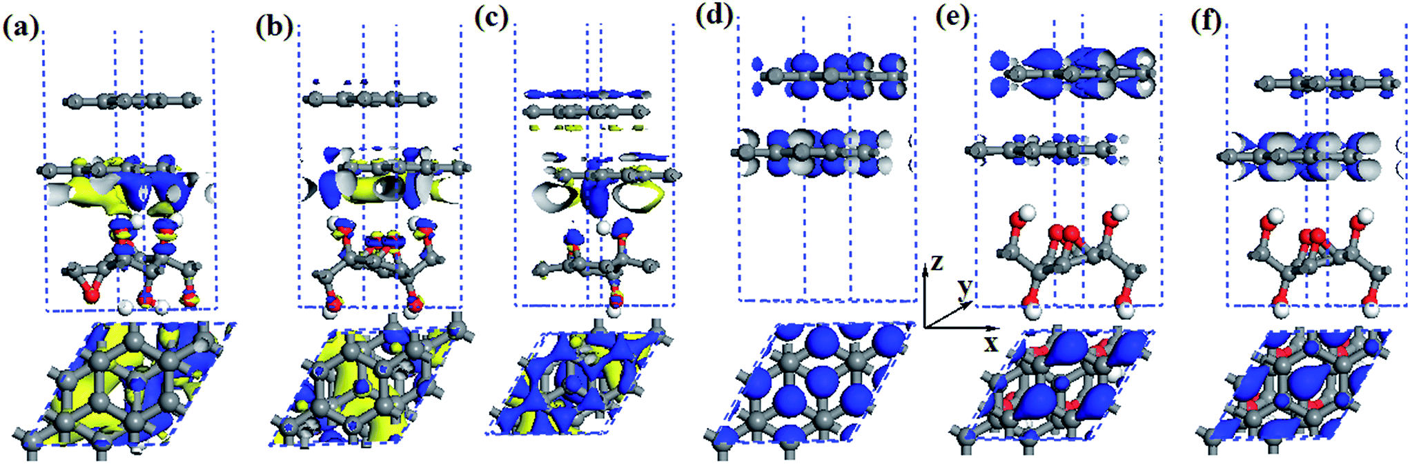 | ||
| Fig. 5 Charge density difference of BG supported on (a) GO-2O-4OH-1, (b) GO-2O-4OH-2, and (c) GO-O-2OH-2: the blue and yellow areas denote electron accumulation and depletion, respectively, and isosurfaces are 0.001 e Å−3. Isosurface (0.04 e Å−3) plot of particle charge densities for the (d) VBM or CBM of pristine graphene, (e) CBM, and (d) VBM of BG/GO-2O-4OH-2. In (a)–(f), the z direction is perpendicular to graphene bilayer. | ||
From Fig. 5a–c, it clearly shows that the charge densities of BG are redistributed after GOs interaction. The oxygen atoms from all GOs always accumulates electrons transferred from bottom graphene layer, while the carbon atoms of bottom graphene layer can lose and/or accumulate electrons, depending on the structure of GOs substrate. This results lead to coexistence of electron-rich and hole-rich regions on the bottom graphene layer. The charge transfer in the interface of BG/GO-2O-4OH-1 (Fig. 5a) is slightly more apparent, compared to other two GOs (Fig. 5b and c) due to the shorter interlayer spacing for the former. According to the charge density difference and the corresponding band gap (74 meV for GO-2O-4OH-1, 230 meV for GO-2O-4OH-2, and 245 meV for GO-O-2OH-2), it is difficult to find any positive correlation between the opened band gap value in BG and the charge transfers.
The charge transfers from GOs to its neighboring graphene layer break the symmetry balance of two graphene layers, leading to band gap opening. Thus, we analysed the partial charge densities of VBM and CBM of pristine BG and BG/GO-2O-4OH-2. As shown in Fig. 5d, for the pristine BG, the carbon atoms from two graphene layers have equivalent contribution to the Dirac point (DP). However, when BG is supported on GOs, the electronic states of CBM and VBM are contributed by two different graphene layer: the former mainly comes from the pz orbitals of carbon atoms of the upper graphene layer (Fig. 5e), while the latter be from the bottom layer (Fig. 5f).
To further insight into the charge transfer, we plots the planar averaged charge density difference along the z direction perpendicular to the bilayer graphene for selected systems as shown in Fig. 6. The positive and negative values represent the electron accumulation and depletion, respectively. It is clear that besides the interlayer regions between GOs and bottom graphene layer, the interface between BG appears two significant peaks: one located at about 8 Å in z direction corresponds to the electron accumulation, the other at about 9.5 Å belongs to the electron depletion. Based on these data and the band gaps as shown in Table 1, it seems to be that the larger the electron accumulation and depletion in these two peaks, the larger the band gap one can obtain. Therefore, the value of band gap in BG is well correlated to the charge transfers from the interface between upper and bottom graphene layers.
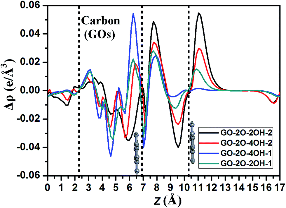 | ||
| Fig. 6 The profile of the planar averaged charge density difference for the BG/GOs hybrids as a function of position in the z-direction. The vertical dashed lines denote the central location of atomic layer of the BG and carbon atoms of GOs. | ||
The remarkable charge transfers can induce the formation of an effective electronic field in BG. The magnitude of built-in electric field depends on the structure of GOs substrate, determining the band gap value in BG. As reported in previous reports,82 increasing the chemical difference between two degenerated bands at the Fermi level is a very important factor for opening the energy gap in the graphene systems. To illuminate this correlation, we calculated the electrostatic potential of selected BG/GOs systems. As shown in Fig. 7, the effective electronic field of BG/GO-2O-2OH-2 (Fig. 7b) and GO-2O-4OH-2 (Fig. 7d) is more distinct, compared to the GO-2O-2OH-1 (Fig. 7a) and GO-2O-4OH-1 (Fig. 7c) substrates. We use the difference in core-level electrostatic potential (corresponding to two highest points in potential of each BG/GOs nanocomposite) to represent the chemical difference. These values are 2.52 (Fig. 6a), 7.96 (Fig. 6b), 2.34 (Fig. 6c), and 5.22 eV (Fig. 6d), implying a positive correlation with the band gaps of 89, 261, 74, and 230 meV. Thus, we obtain a promising way to open a sizeable band gap in BG but retain its intrinsic electronic properties using the highly stable GOs as substrate.
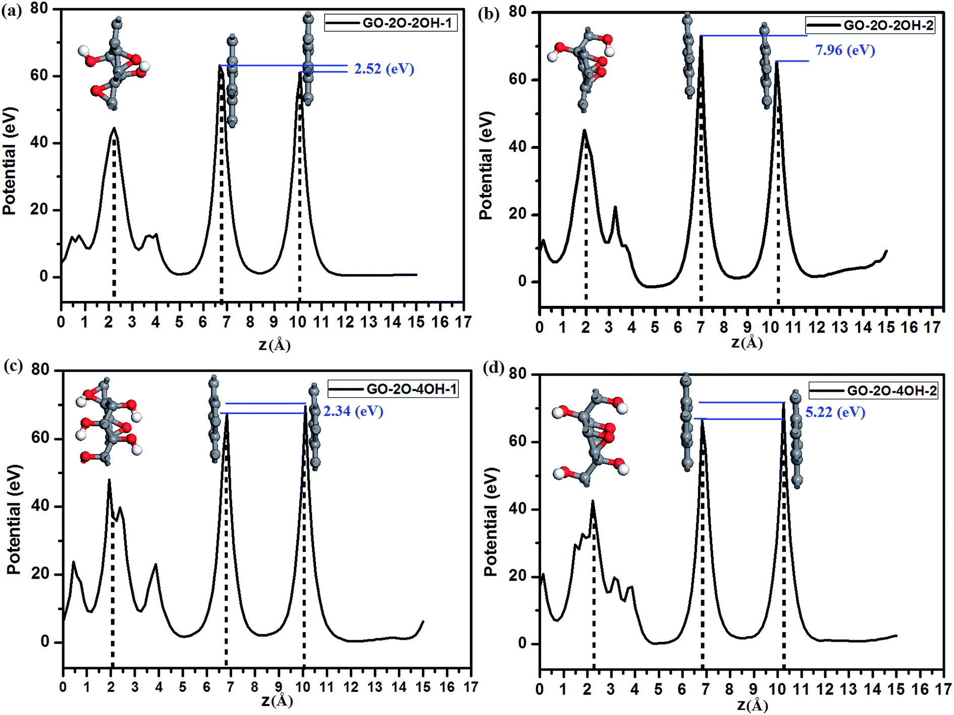 | ||
| Fig. 7 The xy-averaged electrostatic potential of BG/GOs nanocomposites as a function of position in the z-direction. The vertical dashed lines denote the central location of atomic layer of the BG and carbon atoms of GOs. The potential difference between graphene bilayer is marked with the blue number. | ||
4. Conclusions
In summary, we performed first-principles calculations to study the electronic properties of BG adsorbed on GOs substrates. Our results show that in contrast to the metallic properties of oxidated BG, the highly stable GOs support can open the band gap in BG, whose values are determined by controlling the structures of GOs. The coexistence of the epoxy and hydroxyl groups on GOs can further increase the band gap in BG to 260 meV. The effective p-type doping of BG is realized as the GOs substrates only contain single epoxides. More importantly, the high μe value in supported BG can be largely maintained. The band gap opening in BG may be attributed to the charge transfers from GOs to bottom graphene layer, which produces a significant chemical difference between two graphene layers. Thus, BG supported on highly stable GOs may present a new way for fabricating high-performance graphene-based nanodevices.Acknowledgements
This work was supported by the National Science Foundation of China (21463004 and 51463002), the Educational Commission of Jiangxi Province (14653), and Jiangxi Provincial Natural Science Foundation (20151BAB203015), the Scientific Research Foundation of Graduate School of Gannan Normal University (YCX15B004). We thank the computational resources and assistance provided by the State Key Laboratory of Physical Chemistry of Solid Surfaces (Xiamen University).References
- A. K. Geim and K. S. Novoselov, Nat. Mater., 2007, 6, 183 CrossRef CAS PubMed.
- A. H. Castro Neto, F. Guinea, N. M. R. Peres, K. S. Novoselov and A. K. Geim, Rev. Mod. Phys., 2009, 81, 109 CrossRef CAS.
- K. S. Novoselov, A. K. Geim, S. V. Morozov, D. Jiang, Y. Zhang, S. V. Dubonos, I. V. Grigorieva and A. A. Firsov, Science, 2004, 306, 666–669 CrossRef CAS PubMed.
- X. Du, I. Skachko, A. Barker and E. Y. Andrei, Nat. Nanotechnol., 2008, 3, 491–495 CrossRef CAS PubMed.
- S. V. Morozov, K. S. Novoselov, M. I. Katsnelson, F. Schedin, D. C. Elias, J. A. Jaszczak and A. K. Geim, Phys. Rev. Lett., 2008, 100, 016602 CrossRef CAS PubMed.
- W. Zhang, C.-T. Lin, K.-K. Liu, T. Tite, C.-Y. Su, C.-H. Chang, Y.-H. Lee, C.-W. Chu, K.-H. Wei, J.-L. Kuo and L.-J. Li, ACS Nano, 2011, 5, 7517–7524 CrossRef CAS PubMed.
- F. Xia, D. B. Farmer, Y. Lin and P. Avouris, Nano Lett., 2010, 10, 715–718 CrossRef CAS PubMed.
- J.-C. Charlier, X. Gonze and J.-P. Michenaud, Phys. Rev. B: Condens. Matter Mater. Phys., 1993, 47, 16162 CrossRef CAS.
- S.-H. Cheng, K. Zou, F. Okino, H. R. Gutierrez, A. Gupta, N. Shen, P. C. Eklund, J. O. Sofo and J. Zhu, Phys. Rev. B: Condens. Matter Mater. Phys., 2010, 81, 205435 CrossRef.
- J. T. Robinson, J. S. Burgess, C. E. Junkermeier, S. C. Badescu, T. L. Reinecke, F. K. Perkins, M. K. Zalalutdniov, J. W. Baldwin, J. C. Culbertson, P. E. Sheehan and E. S. Snow, Nano Lett., 2010, 10, 3001–3005 CrossRef CAS PubMed.
- R. R. Nair, W. Ren, R. Jalil, I. Riaz, V. G. Kravets, L. Britnell, P. Blake, F. Schedin, A. S. Mayorov, S. Yuan, M. I. Katsnelson, H.-M. Cheng, W. Strupinski, L. G. Bulusheva, A. V. Okotrub, I. V. Grigorieva, A. N. Grigorenko, K. S. Novoselov and A. K. Geim, Small, 2010, 6, 2877 CrossRef CAS PubMed.
- Y.-W. Son, M. L. Cohen and S. G. Louie, Phys. Rev. Lett., 2006, 97, 216803 CrossRef PubMed.
- Y.-W. Son, M. L. Cohen and S. G. Louie, Nature, 2006, 444, 347–349 CrossRef CAS PubMed.
- V. Barone, O. Hod and G. E. Scuseria, Nano Lett., 2006, 6, 2748–2754 CrossRef CAS PubMed.
- M. Ezawa, Phys. Rev. B: Condens. Matter Mater. Phys., 2006, 73, 045432 CrossRef.
- Z. Liu, L. Ma, G. Shi, W. Zhou, Y. Gong, S. Lei, X. Yang, J. Zhang, J. Yu, K. P. Hackenberg, A. Babakhani, J.-C. Idrobo, R. Vajtai, J. Lou and P. M. Ajayan, Nat. Nanotechnol., 2013, 8, 119–124 CrossRef CAS PubMed.
- P. Sutter, Y. Huang and E. Sutter, Nano Lett., 2014, 14, 4846–4851 CrossRef CAS PubMed.
- K. Yan, D. Wu, H. Peng, L. Jin, Q. Fu, X. Bao and Z. Liu, Nat. Commun., 2012, 3, 1280 CrossRef PubMed.
- N. Cuong, M. Otani and S. Okada, Phys. Rev. Lett., 2011, 106, 106801 CrossRef PubMed.
- S. Y. Zhou, G.-H. Gweon, A. V. Fedorov, P. N. First, W. A. d. Heer, D.-H. Lee, F. Guinea, A. H. C. Neto and A. Lanzara, Nat. Mater., 2007, 6, 770 CrossRef CAS PubMed.
- G. Giovannetti, P. A. Khomyakov, G. Brocks, P. J. Kelly and J. v. d. Brink, Phys. Rev. B: Condens. Matter Mater. Phys., 2007, 76, 073103 CrossRef.
- J.-H. Chen, C. Jang, S. Xiao, M. Ishigami and M. S. Fuhrer, Nat. Nanotechnol., 2008, 3, 206–209 CrossRef CAS PubMed.
- L. A. Ponomarenko, R. Yang, T. M. Mohiuddin, M. I. Katsnelson, K. S. Novoselov, S. V. Morozov, A. A. Zhukov, F. Schedin, E. W. Hill and A. K. Geim, Phys. Rev. Lett., 2009, 102, 206603 CrossRef CAS PubMed.
- Z. Liu, L. Song, S. Zhao, J. Huang, L. Ma, J. Zhang, J. Lou and P. M. Ajayan, Nano Lett., 2011, 11, 2032–2037 CrossRef CAS PubMed.
- C. R. Dean, A. F. Young, I. Meric, C. Lee, L. Wang, S. Sorgenfrei, K. Watanabe, T. Taniguchi, P. Kim, K. L. Shepard and J. Hone, Nat. Nanotechnol., 2010, 5, 722–726 CrossRef CAS PubMed.
- J. Xue, J. Sanchez-Yamagishi, D. Bulmash, P. Jacquod, A. Deshpande, K. Watanabe, T. Taniguchi, P. Jarillo-Herrero and B. J. LeRoy, Nat. Mater., 2011, 10, 282–285 CrossRef CAS PubMed.
- X. Li, Y. Dai, Y. Ma, S. Han and B. Huang, Phys. Chem. Chem. Phys., 2014, 16, 4230–4235 RSC.
- K. F. Mak, C. H. Lui, J. Shan and T. F. Heinz, Phys. Rev. Lett., 2009, 102, 56405 CrossRef PubMed.
- J. B. Oostinga, H. B. Heersche, X. Liu, A. F. Morpurgo and L. M. K. Vandersypen, Nat. Mater., 2007, 7, 151–157 CrossRef PubMed.
- M. Aoki and H. Amawashi, Solid State Commun., 2007, 142, 123–127 CrossRef CAS.
- Y. Zhang, T.-T. Tang, C. Girit, Z. Hao, M. C. Martin, A. Zettl, M. F. Crommie, Y. R. Shen and F. Wang, Nature, 2009, 459, 820–823 CrossRef CAS PubMed.
- T. Ohta, A. Bostwick, T. Seyller, K. Horn and E. Rotenberg, Science, 2006, 313, 951–954 CrossRef CAS PubMed.
- I. Gierz, C. Riedl, U. Starke, C. R. Ast and K. Kern, Nano Lett., 2008, 8, 4603–4607 CrossRef CAS PubMed.
- L. S. Panchakarla, K. S. Subrahmanyam, S. K. Saha, A. Govindaraj, H. R. Krishnamurthy, U. V. Waghmare and C. N. R. Rao, Adv. Mater., 2009, 21, 4726–4730 CAS.
- S.-O. Guillaume, B. Zheng, J.-C. Charlier and L. Henrard, Phys. Rev. B: Condens. Matter Mater. Phys., 2012, 85, 035444 CrossRef.
- M. G. Menezes and R. B. Capaz, Phys. Rev. B: Condens. Matter Mater. Phys., 2010, 82, 245414 CrossRef.
- P. A. Denis and F. Iribarne, Chem. Phys. Lett., 2016, 658, 152–157 CrossRef CAS.
- Y. Mao and J. Zhong, Nanotechnology, 2008, 19, 205708 CrossRef PubMed.
- Y. Mao, G. M. Stocks and J. Zhong, New J. Phys., 2010, 12, 033046 CrossRef.
- S. J. Gong, W. Sheng, Z. Q. Yang and J. H. Chu, J. Phys.: Condens. Matter, 2010, 22, 245502 CrossRef CAS PubMed.
- H. Pinto, R. Jones, J. P. Goss and P. R. Briddon, Phys. Rev. B: Condens. Matter Mater. Phys., 2010, 82, 125407 CrossRef.
- S. Zhao and J. Xue, Phys. Rev. B: Condens. Matter Mater. Phys., 2012, 86, 165428 CrossRef.
- X. Tian, J. Xu and X. Wang, J. Phys. Chem. B, 2010, 114, 11377–11381 CrossRef CAS PubMed.
- T. H. Wang, Y. F. Zhu and Q. Jiang, J. Phys. Chem. C, 2013, 117, 12873–12881 CAS.
- D. L. Duong, S. M. Lee, S. H. Chae, Q. H. Ta, S. Y. Lee, G. H. Han, J. J. Bae and Y. H. Lee, Phys. Rev. B: Condens. Matter Mater. Phys., 2012, 85, 205413 CrossRef.
- S. Tang, J. Yu and L. Liu, Phys. Chem. Chem. Phys., 2013, 15, 5067–5077 RSC.
- J. Hao, C. Huang, H. Wu, Y. Qiu, Q. Gao, Z. Hu, E. Kan and L. Zhang, Nanoscale, 2015, 7, 17096–17101 RSC.
- S. Watcharotone, D. A. Dikin, S. Stankovich, R. Piner, I. Jung, G. H. B. Dommett, G. Evmenenko, S.-E. Wu, S.-F. Chen, C.-P. Liu, S. T. Nguyen and R. S. Ruoff, Nano Lett., 2007, 7, 1888–1892 CrossRef CAS PubMed.
- G. Eda, G. Fanchini and M. Chhowalla, Nat. Nanotechnol., 2008, 3, 270–274 CrossRef CAS PubMed.
- H. A. Becerril, J. L. Mao, Z. R. M. Stoltenberg, Z. Bao and Y. Chen, ACS Nano, 2008, 2, 463–470 CrossRef CAS PubMed.
- T. Musso, P. V. Kumar, A. S. Foster and J. C. Grossman, ACS Nano, 2014, 8, 11432–11439 CrossRef CAS PubMed.
- L. Xu, W.-Q. Huang, L.-L. Wang, Z.-A. Tian, W. Hu, Y. Ma, X. Wang, A. Pan and G.-F. Huang, Chem. Mater., 2015, 27, 1612–1621 CrossRef CAS.
- A. Nourbakhsha, M. Cantoroa, A. V. Klekacheva, G. Pourtoisa, J. Hofkense, M. H. v. d. Veena, M. M. Heynsa, S. D. Gendta and B. F. Selsb, J. Phys. Chem. C, 2011, 115, 16619–16624 Search PubMed.
- L. Zhu, J. Wang and F. Ding, J. Phys. Chem. C, 2012, 116, 8027–8033 CAS.
- Y. Ma, Y. Dai, M. Guo and B. Huang, Phys. Rev. B: Condens. Matter Mater. Phys., 2012, 85, 235448 CrossRef.
- Y. Li and Z. Chen, J. Phys. Chem. Lett., 2013, 4, 269–275 CrossRef CAS PubMed.
- M. D. Segall, P. J. D. Lindan, M. J. Probert, C. J. Pickard, P. J. Hasnip, S. J. Clark and M. C. Payne, J. Phys.: Condens. Matter, 2002, 14, 2717 CrossRef CAS.
- J. P. Perdew, K. Burke and M. Ernzerhof, Phys. Rev. Lett., 1996, 77, 3865 CrossRef CAS PubMed.
- S. Grimme, J. Comput. Chem., 2006, 27, 1787–1799 CrossRef CAS PubMed.
- D. Vanderbilt, Phys. Rev. B: Condens. Matter Mater. Phys., 1990, 41, 7892 CrossRef.
- G. Eda, Y.-Y. Lin, S. Miller, C.-W. Chen, W.-F. Su and M. Chhowalla, Appl. Phys. Lett., 2008, 92, 233305 CrossRef.
- J. Wu, H. A. Becerril, Z. Bao, Z. Liu, Y. Chen and P. Peumans, Appl. Phys. Lett., 2008, 92, 263302 CrossRef.
- W. Cai, R. D. Piner, F. J. Stadermann, S. Park, M. A. Shaibat, Y. Ishii, D. Yang, A. Velamakanni, S. J. An, M. Stoller, J. An, D. Chen and R. S. Ruoff, Science, 2008, 321, 1815–1817 CrossRef CAS PubMed.
- A. Bagri, R. Grantab, N. V. Medhekar and V. B. Shenoy, J. Phys. Chem. C, 2010, 114, 12053–12061 CAS.
- A. Bagri, C. Mattevi, M. Acik, Y. J. Chabal, M. Chhowalla and V. B. Shenoy, Nat. Chem., 2010, 2, 581–587 CrossRef CAS PubMed.
- J.-A. Yan, L. Xian and M. Y. Chou, Phys. Rev. Lett., 2009, 103, 086802 CrossRef PubMed.
- W. Zhang, V. Carravetta, Z. Li, Y. Luo and J. Yang, J. Chem. Phys., 2009, 131, 244505 CrossRef PubMed.
- Z. Li, W. Zhang, Y. Luo, J. Yang and J. G. Hou, J. Am. Chem. Soc., 2009, 131, 6320–6321 CrossRef CAS PubMed.
- A. Lerf, H. He, M. Forster and J. Klinowski, J. Phys. Chem. B, 1998, 102, 4477–4482 CrossRef CAS.
- X. Li, G. Zhang, X. Bai, X. Sun, X. Wang, E. Wang and H. Dai, Nat. Nanotechnol., 2008, 3, 538–542 CrossRef CAS PubMed.
- W. Gao, L. B. Alemany, L. Ci and P. M. Ajayan, Nat. Chem., 2009, 1, 403–408 CrossRef CAS PubMed.
- J.-A. Yan and M. Y. Chou, Phys. Rev. B: Condens. Matter Mater. Phys., 2010, 82, 125403 CrossRef.
- H.-K. Jeong, Y. P. Lee, R. J. W. E. Lahaye, M.-H. Park, K. H. An, I. J. Kim, C.-W. Yang, C. Y. Park, R. S. Ruoff and Y. H. Lee, J. Am. Chem. Soc., 2008, 130, 1362–1366 CrossRef CAS PubMed.
- K.-Y. Lian, Y.-F. Ji, X.-F. Li, M.-X. Jin, D.-J. Ding and Y. Luo, J. Phys. Chem. C, 2013, 117, 6049–6054 CAS.
- D. W. Boukhvalov and M. I. Katsnelson, J. Am. Chem. Soc., 2008, 130, 10697–10701 CrossRef CAS PubMed.
- R. J. W. E. Lahaye, H. K. Jeong, C. Y. Park and Y. H. Lee, Phys. Rev. B: Condens. Matter Mater. Phys., 2009, 79, 125435 CrossRef.
- A. Ramasubramaniam, D. Naveh and E. Towe, Nano Lett., 2011, 11, 1070–1075 CrossRef CAS PubMed.
- J. Bardeen and W. Shockley, Phys. Rev., 1950, 80, 72–80 CrossRef CAS.
- X. Li, Y. Dai, M. Li, W. Wei and B. Huang, J. Mater. Chem. A, 2015, 3, 24055–24063 CAS.
- P. E. Trevisanutto, C. Giorgetti, L. Reining, M. Ladisa and V. Olevano, Phys. Rev. Lett., 2008, 101, 226405 CrossRef PubMed.
- X. Ma, Y. Dai, L. Yu and B.-B. Huang, Light: Sci. Appl., 2016, 5, e16017 CrossRef CAS.
- E. Kan, H. Ren, F. Wu, Z. Li, R. Lu, C. Xiao, K. Deng and J. Yang, J. Phys. Chem. C, 2012, 116, 3142–3146 CAS.
Footnote |
| † Electronic supplementary information (ESI) available: Charge transfers of BG/GOs with different sampling space, optimized structures and calculated results for other stacking order and other configuration, and the corresponding band structures. See DOI: 10.1039/c7ra01134b |
| This journal is © The Royal Society of Chemistry 2017 |