DOI:
10.1039/C7RA01117B
(Paper)
RSC Adv., 2017,
7, 16655-16661
Study on fracture behavior of individual InAs nanowires using an electron-beam-drilled notch†
Received
25th January 2017
, Accepted 9th March 2017
First published on 15th March 2017
Abstract
The mechanical properties and fracture behavior of individual InAs nanowires (NWs) were investigated under uniaxial tensile loading in a transmission electron microscope. The InAs NWs exhibited elastic deformation during the tensile test till fracture and the experiments revealed a brittle fracture on the (111) plane of a zinc-blende structure. Hemi-ellipse-shaped notches with various radii of curvature, formed via a focused electron beam, were utilized to investigate the fracture behavior when there is a structural flaw at the nanometer scale. The dimensions of notches are controlled with proper understanding of electron beam irradiation on the InAs material system. The stress concentration phenomena with dependence on the notch size are demonstrated in the InAs NWs by analyzing the results from a finite element method simulation.
Introduction
III-As nanowires (NWs) among one-dimensional (1D) nanostructures (nanowires, nanotubes, nanorods, etc.) have been the subject of much research because they are often considered to be the active components of electrical and optical nanodevices.1–5 III-As NWs have been also recently suggested as an element for novel electromechanical nanodevices due to the specific response of current to strain.6,7 The reliability of such nanodevices becomes important because of the low dimensionality as well as overall size of the devices. Therefore, characterization and understanding of the mechanical properties of III-As NWs is essential for designing, fabricating, and operating such nanodevices. Strangely, the fracture behavior among various mechanical properties of 1D nanostructures has not been systematically evaluated to date although it is one of the most important mechanical properties of any material; a property that describes the ability of a material to resist fracturing from a crack must be considered at the design stage for exact nanomaterial applications. The importance of the evaluation of mechanical properties of 1D nanostructures has been emphasized by many researchers.8–13 However, the precise characterization of mechanical properties of nanostructures is often considered to be challenging mostly because of its limited dimension, resulting in difficulty to find all-in-one instruments/methods which can handle and manipulate the nanostructures and enable to observe and measure properties with enough spatial resolution. Several attempts have been made in recent years to correctly measure the mechanical properties of nanostructures with a variety of techniques, such as dynamic resonance in electron stroboscopy,14 probe-based compressive and tensile testing using transmission electron microscopy (TEM),6,15,16 and atomic force microscopy (AFM).17,18 Table S1† summarizes recent experimental studies on mechanical properties of InAs NWs, based on various electron microscopy techniques.14,17,18 Most of the reports have focused on determining elastic or bending moduli of InAs NWs; however, fracture property has not been investigated in InAs NWs. A reliable and systematic evaluation of fracture behavior is essential for InAs NWs at the component level in order to achieve novel high-performance nanodevices,3,19–22 as already mentioned above. In addition, for detailed understanding of fracture behaviors, microstructural characterization of InAs NWs is also required because the fracture behaviors are intimately related to microstructural properties.
Here we demonstrate a novel approach to evaluate the mechanical and fracture characteristics of individual InAs NWs in TEM using a focused electron beam (FEB) as a tool to make notches. The FEB enables to produce controllable notches and to perform the evaluation of fracture behaviors. We discuss the microstructural evolution during fracturing of InAs NWs and demonstrate the stress-concentration phenomena, with the aid of finite element method (FEM) simulation.
Experimental
Sample preparation
InAs NWs, with a diameter ranged from 50 to 120 nm, were grown on a Si (111) substrate by molecular beam epitaxy (MBE) without a metal catalyst. Prior to the growth, a Si (111) substrate was sequentially cleaned with acetone and methanol solution and then deoxidized by using hydrofluoric acid solution. The growth temperature of the InAs NWs was 430 °C. The In and As fluxes were 3 × 10⁻⁸ and 1.2 × 10⁻⁵ Torr, respectively. After the growth, the InAs NWs were separated from the Si substrate and dispersed in methanol solution by ultra-sonication. The methanol solution with the InAs NWs was dropped onto a reduced anodic aluminum oxide membrane. After drying the methanol, a single InAs NW was transferred on a push-to-pull (PTP) device (Picoindenter; Hysitron, Inc.) for the measurement of mechanical properties (Fig. S1†). For the transfer of a single NW, a homemade transfer system, composed of an optical microscope and a manipulator with a sharp metal probe, was used in our experiment. A single InAs NW was fixed on the PTP device by epoxy, which has an advantage over Pt metal by using a focused ion beam (FIB) system as a clamping material because physical damages on the edge of the NW during the electron-beam-induced deposition process can be avoided with epoxy. All of the NWs tested in our experiment were aligned to the loading axis of the PTP device (<3° from the axis).
Mechanical testing and simulation
Microstructural characterization and mechanical measurements were performed in a TEM (FEI Tecnai G2 F30 S/TEM; FEI Company). For fracture tests, notches with various sizes were formed on the InAs NWs by using a FEB in the TEM operated at 300 keV; the exposure dose for the FEB was 3.99 C cm−2. The PTP device was pulled with a displacement rate of 20 nm s−1 for imposing tensile strain on the InAs NWs. The displacement in the InAs NWs was measured from a series of TEM images captured by TV rate camera. FEM simulations on the tensile test of the InAs NWs with and without notches were conducted using a ABAQUS software. The element type of quadratic C3D20 with a 20-node and full integration was adopted and the boundary conditions were as follows: (1) the displacement at one end of a NW was fixed (i.e., X = 0, Y = 0, and Z = 0) and (2) the other end of the NW was tensioned along the longitudinal direction.
Results and discussion
Microstructure of InAs NWs
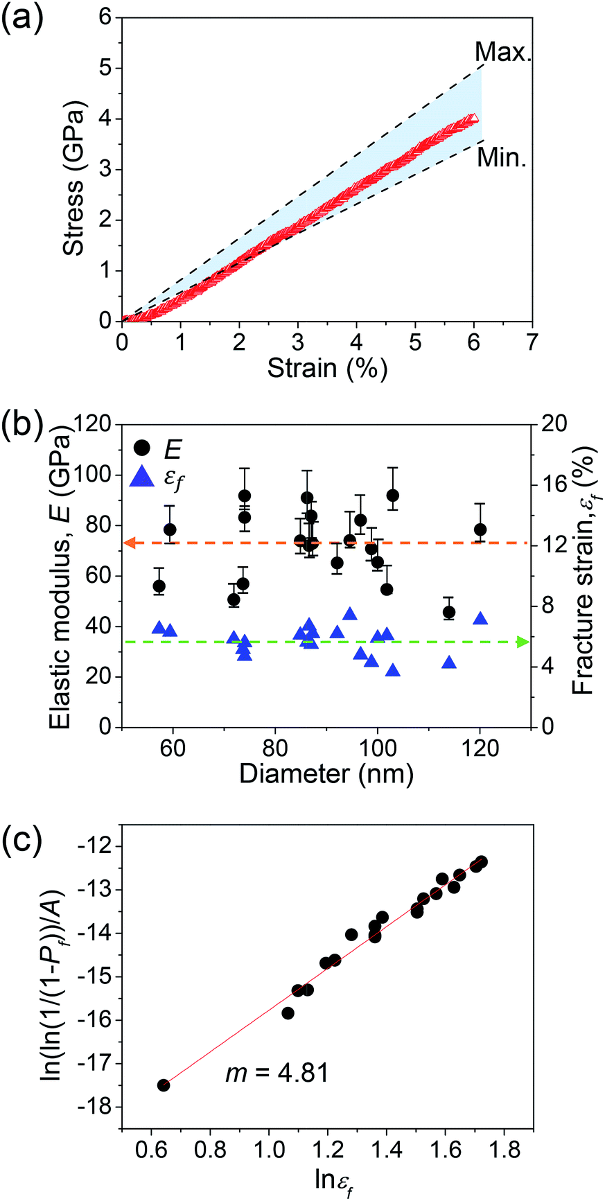
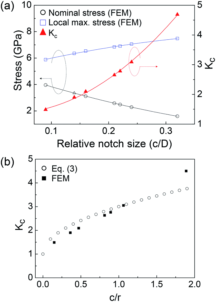
Fig. 1 shows the representative microstructures of InAs NWs used for tensile tests in this work. A bright-field TEM (BF-TEM) image shows an InAs NW placed on the gap of a PTP device (Fig. 1a). The InAs NW is aligned to the loading axis of the PTP device with less than 2 degrees of tilting. The InAs NW has a uniform diameter of 80 nm. Many stacking faults in {111} crystallographic planes, which is perpendicular to the growth direction, were observed, as shown in the high-resolution TEM (HR-TEM) image in Fig. 1b. The InAs NW has a hexagonal cross-section, bounded by the {220} planes of a zinc-blende (ZB) structure (Fig. 1c and d), and it is found that the NW grows along the 〈111〉 direction, as shown in selected-area electron diffraction (SAED) patterns of Fig. 1d–f. The strong streaks, perpendicular to the stacking faults, in the SAED pattern (Fig. 1e inset) also agree with the existence of the stacking faults on the {111} planes. It is well known that these {111}-stacking faults are easily formed in InAs NWs system.23,24 The precise measurement of the dimension of nanomaterials is important for quantitatively attaining the mechanical properties in a nanometer-sized regime. Especially, defining a cross-sectional area is important for evaluating the mechanical properties, because the stress value is determined using the cross-section area (see eqn (1) below).
 |
| | Fig. 1 (a) A BF-TEM image of an InAs NW aligned to the loading axis of a PTP device. (b) A HR-TEM image of the InAs NW. The stacking sequence (letters and circles) of the atomic layers shows it grows along the 〈111〉 direction and has a ZB structure with many stacking faults. (c and d) BF-TEM and HR-TEM images of the cross-section of an InAs NW. The InAs NW has a hexagonal cross-section, faceted by the {220} planes (see inset in d). (e and f) BF-TEM images of two different InAs NWs, which have different crystallographic orientations along the electron beam. The SAED patterns in e and f show that they are aligned along the [![[1 with combining macron]](https://www.rsc.org/images/entities/char_0031_0304.gif) 10] and [2] directions, respectively. The InAs NWs show distinct image contrasts with the crystallographic orientation, as shown in the intensity profiles across the NWs (right panels of e and f). 10] and [2] directions, respectively. The InAs NWs show distinct image contrasts with the crystallographic orientation, as shown in the intensity profiles across the NWs (right panels of e and f). | |
It is possible to extract meaningful data in TEM by selecting the proper electron-beam direction. In our experiments, all of the InAs NWs were tilted and aligned to the [10] direction, as shown in Fig. 1e. It is found that the NWs in most cases tend to arrange in the [10] direction. The alignment of the NW as shown in Fig. 1f was rarely observed. The cross-sectional area was calculated by considering the geometry based on the images and diffraction patterns, as shown in Fig. 1e and f. In Fig. 1e and f, the contrast line profiles are good agreement of the expected geometry. Based on these characteristic relationships between the electron beam direction and the geometric shape of the NWs, the exact cross-sectional area was calculated to obtain the correct mechanical parameters. The InAs NWs aligned on PTP devices as shown in Fig. 1e were selected to study the size dependence of mechanical properties in our experiment. The area was defined in the same way as shown in Fig. 1e and the tilting angle of the NWs and the ratio of s to D in Fig. 1e were considered to be uncertainty parameters in determining the exact area of the NWs. It should also be noted that the InAs NW observed along the [2] direction of the ZB structure seems like being free from planar defects (Fig. 1f).
Mechanical test and fracture behavior of InAs NWs without a notch
The change in the InAs NWs during tensile testing was monitored by a real-time TEM observation. The continuous change of the black-and-white contrast bands in the InAs NWs during the in situ measurement proves the variation of strain; this is related to the change of local atomic structures resulting from the strain in the NW (see Video S1†).15,16,25 A rough surface was observed on the fractured end of the InAs NW. Atomic rearrangements were also observed at the end of the InAs NW after fracturing (Fig. S2†). It appears that this observation differs from those reported in other nanowires.26,27 The strong stress may be concentrated at the moment at which the fracture is triggered by tensile loading and atomic rearrangement at the fracture plane could result from the stress by converting to thermal energy.28–30
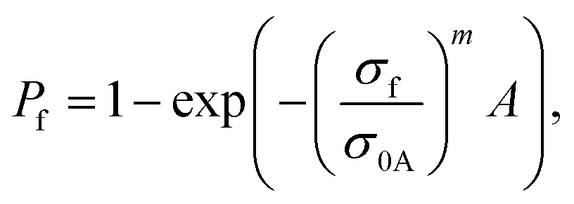
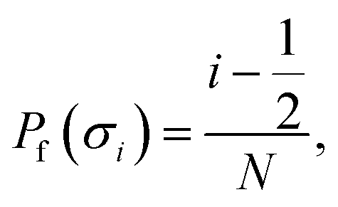
Fig. 2a shows a representative stress (σ)–strain (ε) curve for the InAs NW without a notch. The tensile stress increases linearly with the increase of displacement until the fracture is initiated. The linear σ–ε curve indicates that the InAs NW undergoes elastic deformation during the tensile test. An abrupt load drop with the fracture also indicates brittle fracture. Because the PTP device is designed to act as an elastic body, it is possible to obtain the elastic modulus, E, of the InAs NWs by considering the spring constant of the PTP device in the displacement–load curves with a linear relation. The stress can be derived by applying the elastic stress–strain relationship σ = Eε. The elastic modulus, the fracture strain (εf), and the tensile strength (TS) (of which the measured InAs NWs is the same as the yield strength) were determined from twenty NWs (see Table S2†). Fig. 2b shows the elastic modulus and fracture strain as a function of the diameter of the NWs. In our experiments, we found that in the range of 50–120 nm, the elastic behavior is independent on the diameter of the InAs NWs, which is consistent with the previous report.18 The average elastic modulus, Eavg, was 72.0 ± 13.5 GPa. The average fracture strain, εf,avg, was 5.70 ± 0.95%. The fracture strength, σf,avg, is slightly larger than that reported by X. Li et al.18 We consider that this difference may originate from the fact that we clamped the ends of the NWs for the test.18 As mentioned above, because the InAs NWs experienced a brittle fracture, a Weibull-type weakest-link probabilistic model31,32 can be adopted to analyze variation in fracture strength. Specifically, we considered the probability of the existence of weak points on its surface because the InAs NWs were free from internal structural flaws, except stacking faults, to initiate fracture. Classical Weibull statistics31,32 assumes that the probability of failure Pf with surface area A under uniaxial stress is:
| |
 | (1) |
where
σf is the failure strength,
σ0A is the characteristic strength relative to
A, and
m is the Weibull modulus. Probabilities
Pf can be calculated as follows:
| |
 | (2) |
where
N is the total number of specimens tested and the strengths
σ1,
σ2,
σ3, …,
σN are ranked in ascending order.
Fig. 2c shows the classical Weibull statistics applied to the set of fracture-strength data
vis-à-vis the surface area by considering
eqn (1) and
(2). The
m is estimated to be 4.81, while the correlation coefficient is ∼88%. This indicates that fracture strength is associated with the surface area of the nanowires.
 |
| | Fig. 2 (a) Representative σ–ε curve of an InAs NW without a notch. The area, bounded by the dotted lines, indicates the possible range of the elastic modulus of the InAs NW by considering the uncertainty. (b) Elastic moduli (black circles) and fracture strains (blue triangles) of twenty InAs NWs as a function of diameter. The dotted arrows indicate the average values. (c) Plot of the Weibull statistics of InAs NWs. | |
Notch preparation by electron beam drilling
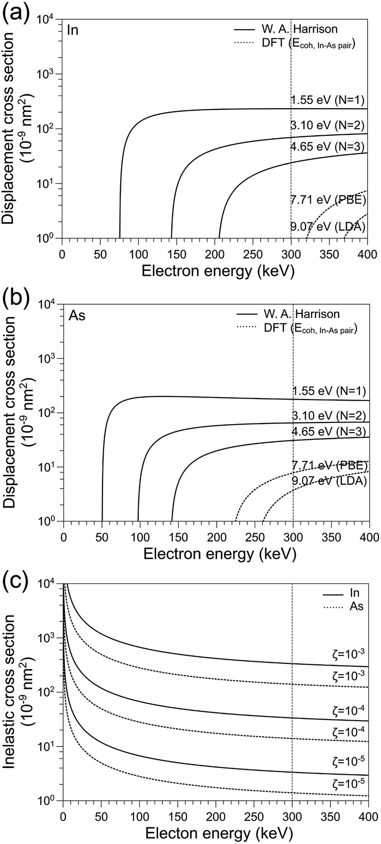
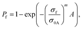
Here, to study the fracture behavior of the InAs NWs, notches with a hemi-ellipsoidal shape (HES)33,34 were generated on the NWs using the FEB. By applying the FEB, it is possible to remove a material from the specimen by controlling direct atomic displacement by inelastic collision and ionization (or radiolysis). An incident electron beam transfers a significant amount of energy to the atoms of the specimen by a direct collision, which can be sufficient to sputter it from the surface.35–37 The displacement cross section for sputtering σd, the probability that an electron displaces the target atom, is estimated using the displacement energy Ed and the maximum displacement energy Emax of InAs. In and As can be seen in Fig. 3a and b, we compared σd using three different Ed values: from the literature38 and density functional theory (DFT) calculations [ESI 3†].39 On the other hand, the cross section of radiolytic movement of atoms in a specimen is related with the ionization or excitation of electrons by inelastic scattering. The cross section of radiolytic movement by inelastic scattering σin is estimated using the threshold energy Eth and the experimental efficiency factor ζ.40–42 Full details of calculation of σd and σin are provided in the ESI 4.†
 |
| | Fig. 3 (a and b) Calculated σd of an In atom and As atom as a function of the E0 (N = number of bonds). (c) σin in InAs by inelastic scattering as ionization or radiolysis as a function of the E0. | |
Fig. 3a and b show the σd for In and As atoms in InAs as a function of the electron beam energy E0 for several Ed. The critical electron energies, Ecr, to sputter In and As atoms out, are depending on the Ed and are in the range of 76–353 keV for In and 50–249 keV for As. The displacement cross-sections for In and As atoms are in the range of 10−9 to 10−6 nm2 in the electron beam energy of 100–400 keV. The σin for InAs as a function of the incident electron energy is shown in Fig. 3c. The σin of InAs is in the range of 10−9 to 10−6 nm2 in the electron beam energy of 100–400 keV. The σin drastically decreases with the increase of the E0.
In this experiment, because the TEM was operated at 300 keV to produce HES notches, As atoms are sputtered out during the electron beam drilling process; but whether In atoms are sputtered out or not will depend on how much the Ed is for an In atom. Both In and As atoms experience radiolysis at 300 keV. In addition, the σd is comparable to the σin, which means that both the sputtering and the radiolytic movement have contributed to the electron beam drilling of InAs NWs. The dependences of the electron-beam-drilling process on the electron beam energy and the current density of the incident electrons were observed in our experiment (see Fig. S3†). Here, we selected efficient but controllable electron beam energy and exposure dose (300 keV, 3.99 C cm−2) to produce notches.
Fracture behaviour of InAs NWs with a notch
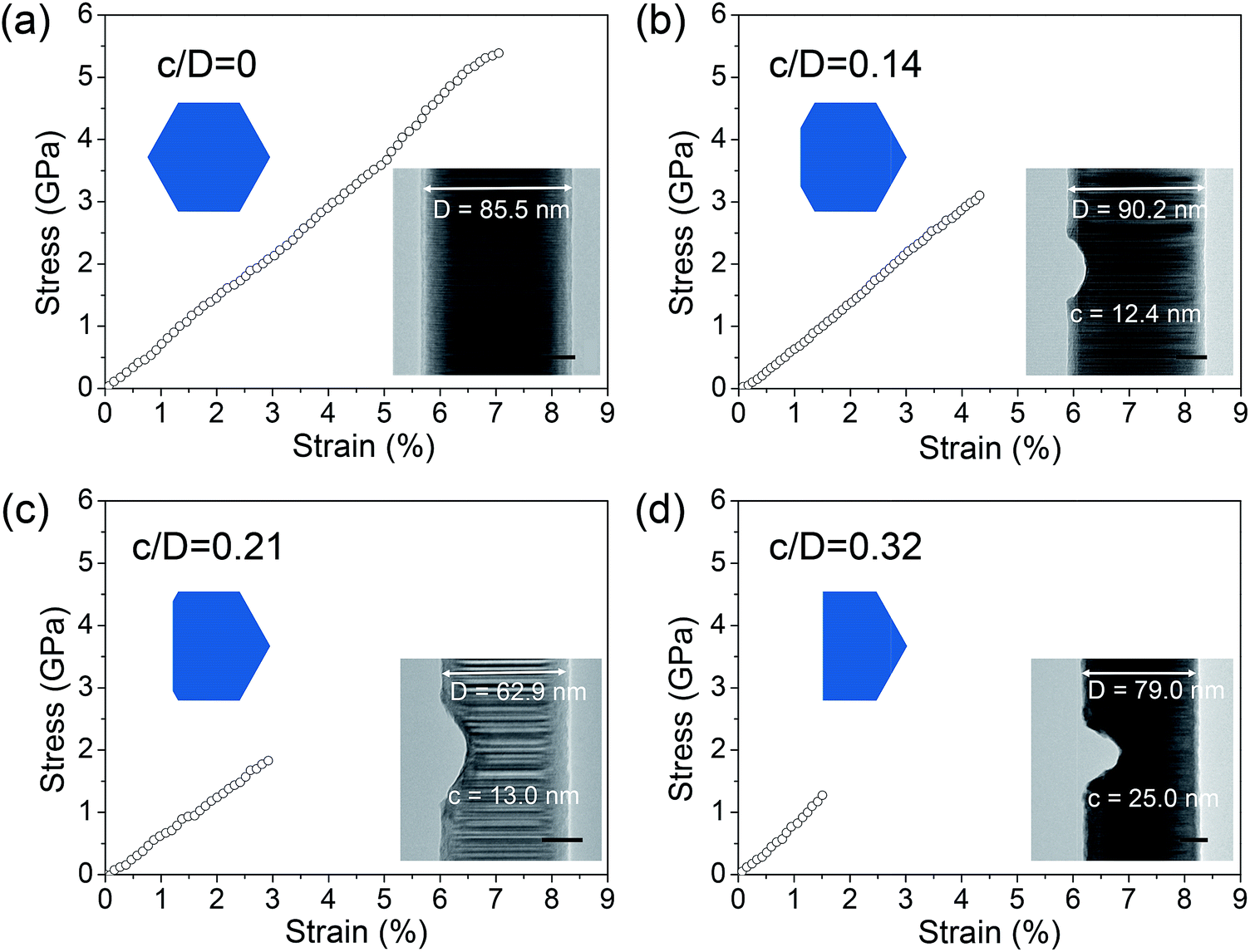
For the study of the fracture behavior and the stress-concentration phenomenon, a schematic diagram of a notch produced in the NWs by the FEB is shown in Fig. S4.† To study fracture behavior, the width (b) of the HES notches was fixed to ∼40 nm, while the depth (c) was controlled (Fig. S4b†). In addition, the diameter (D) of NWs was estimated from TEM images (see Fig. S4b†). The relative notch size was defined as c/D. The mechanical properties of the InAs NWs with a notch were determined by considering the shapes of the NW cross-section at the middle of the notch: its shape varies with the depth of the notches (see Fig. S4c†). With increasing the notch depth, the cross-section changes from a hexagonal to a heptagonal, and to pentagonal shapes, as shown in Fig. S4c.†
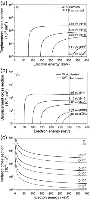
Fig. 4a and b show TEM images captured before and after fracture of an InAs NW with a HES notch, respectively (see Video S2†). It was found that the fracture occurs at the middle of the notch. It means that the stress concentrates at the HES notch on the InAs NW. The magnified TEM images in Fig. 4c and d show two fractured pieces of the InAs NW. Relatively flat surfaces are observed compared with the fracture surface of NWs without a notch. There are no detectable atomic rearrangements in the fracture surfaces; only steps with one or two atomic layers are observed. The TEM results reveal that the brittle fracture initiates at the middle of a notch and propagates along the 〈2〉 directions on the {111} planes.
 |
| | Fig. 4 (a and b) BF-TEM images of an InAs NW with a notch (c/D = 0.14) before and after fracture (scale bar, 500 nm). (c) Magnified BF-TEM image at the fracture surface after a tensile test (scale bar, 20 nm). (d) HR-TEM image showing a flat fracture surface without any atomic structural disorder (scale bar, 2 nm). | |
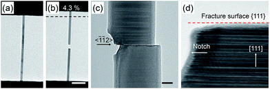
Fig. 5 shows the stress–strain curves of the InAs NWs with several relative notch sizes. The linear stress–strain curves and the abrupt drops of load after fracture also demonstrate that the brittle fracture occurs in the InAs NWs with a notch. Table 1 lists the relative notch size c/D, elastic modulus E, the corresponding fracture strain εf,exp, and normalized fracture stress σf,exp from the test of seven samples. The elastic modulus, estimated from InAs NWs with a notch, is consistent with that from InAs NWs without a notch, as expected (Table S2†). The fracture stress and fracture strain decrease as relative notch size (c/D) increases. For example, average values of fracture stress and fracture strain were measured to be 4.1 GPa and 5.7%, respectively, in the NWs without a notch (Table S2†), while they decreased to 1.7 GPa and 1.5% when the relative notch size was 0.32.
 |
| | Fig. 5 Stress–strain curves for the InAs NWs with different relative notch sizes: (a) 0 (no notch), (b) 0.14, (c) 0.21, and (d) 0.32. The insets show BF-TEM images of the NWs before the tensile test. Scale bars represent 20 nm. | |
Table 1 Experimental fracture stress and fracture strain values from InAs NWs with a notch. Calculated local maximum stress and nominal stress values are also present
| No. |
c/D |
Experiment |
Simulation |
| σf,exp (GPa) |
εf,exp (%) |
σmax (GPa) |
σfn (GPa) |
| 1 |
0.09 |
2.9 |
5.5 |
5.880 |
3.958 |
| 2 |
0.14 |
3.1 |
4.3 |
6.360 |
3.345 |
| 3 |
0.16 |
2.9 |
5.2 |
6.530 |
3.113 |
| 4 |
0.21 |
2.0 |
3.0 |
6.840 |
2.580 |
| 5 |
0.22 |
2.1 |
3.4 |
6.900 |
2.480 |
| 6 |
0.24 |
2.1 |
4.0 |
7.060 |
2.285 |
| 7 |
0.32 |
1.7 |
1.5 |
7.480 |
1.595 |
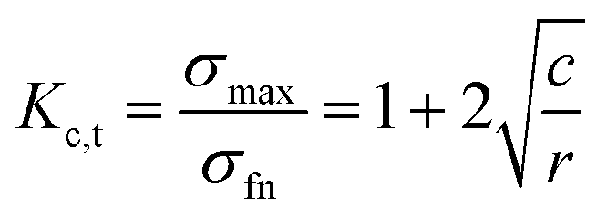
To understand stress distribution and concentration during a tensile test with a notch, we performed FEM simulations of elastic InAs NWs. For simplicity of FEM simulations, we used representative parameters for NWs average diameter and elastic modulus (D = 88.2 nm and E = 72.0 GPa) and adjusted notch sizes using ones in Table 1. The results from the FEM simulations confirmed that stress was concentrated at the middle of the notches (see Fig. S5†). From the FEM simulations, the local maximum stresses, σmax, at the stress-concentration locations and the nominal stresses, σfn, were calculated. Table 1 indicates that the dependence of the measured fracture stresses σf,exp on relative notch size is similar with that of the σfn. Here a stress-concentration factor is defined Kc as σmax/σfn. Fig. 6a shows the σfn, σmax, and Kc curves of FEM simulations as a function of c/D. The Kc nonlinearly increases because the σfn decreases and the σmax increases with the increase of c/D. However, because the Kc is affected by not only the notch size but also the shape of the notches. The Kc was plotted as a function of c/r in Fig. 6b by calculating the curvature radius, r, of the notch with a hemi-elliptical shape (filled squares). The Kc linearly increases with the increase of c/r in Fig. 6b. The stress concentration factor for a hemi-ellipse-shaped notch on a thin element, Kc,t, is calculated by the following equation:43
| |
 | (3) |
where
c is the notch size and
r the radius of curvature at a notch tip. The
Kc,t from
eqn (3) (empty circles) was also plotted in
Fig. 6b for the comparison with the
Kc from the InAs NWs. In
Fig. 6b, the
Kc and
Kc,t values show a different behaviour in the dependence on
c/
r ratio; the
Kc value linearly increases while the
Kc,t nonlinearly increases. This specific behaviour of the
Kc, the stress concentration on the InAs NWs, when compared with the
Kc,t, must be originated from the unique morphology and dimension and the reduced size of the NWs. However, more detailed studies are required to understand the fracture behaviour of NWs because it can be more sensitively affected by the change of the shape and/or the size of defects due to their reduced size.
 |
| | Fig. 6 (a) Simulated nominal stresses, local maximum stresses, and stress concentration factors as a function of the relative notch size, c/D. (b) Stress-concentration factors of FEM simulation and eqn (3), Kc = σmax/σfn, as a function of c/r. | |
Conclusions
The elastic and brittle fracture behaviors of InAs NWs were observed under uniaxial tensile loading via TEM. The shape, dimension, and microstructure of the InAs NWs were carefully characterized to correctly evaluate the mechanical properties of InAs NWs. A rough surface appeared on the fracture plane of the pristine InAs NWs, and atomic rearrangements were detected on the fractured surface. Weibull statistics was applied to ascertain the fracture behavior of the InAs NWs; the Weibull modulus was found to be 4.81. HES notches were created in the InAs NWs by the electron-beam-drilling method to investigate their fracture behavior. The fracture occurred at the center of the notch, which means that this was where the stress concentration was located. We believe that our study suggests a novel route to explore mechanical properties of 1D nanostructures, which can supply the information for the design for the exact application within InAs nanowires in the near future. When using nanowires for a device, it is necessary to consider not only the strength but also the degradation property by the flaw.
Acknowledgements
This work is supported by the R&D Convergence Program of NST (National Research Council of Science & Technology) of Republic of Korea. Work in part supported by “Nano Material Technology Development Program (2014M3A7B6020163) of MSIP/NRF”.
Notes and references
- N. P. Dasgupta, J. Sun, C. Liu, S. Brittman, S. C. Andrews, J. Lim, H. Gao, R. Yan and P. Yang, Adv. Mater., 2014, 26, 2137–2184 CrossRef CAS PubMed.
- A. Casadei, E. F. Pecora, J. Trevino, C. Forestiere, D. Rüffer, E. Russo-Averchi, F. Matteini, G. Tutuncuoglu, M. Heiss, A. Fontcuberta i Morral and L. Dal Negro, Nano Lett., 2014, 14, 2271–2278 CrossRef CAS PubMed.
- G. Koblmüller, K. Vizbaras, S. Hertenberger, S. Bolte, D. Rudolph, J. Becker, M. Döblinger, M.-C. Amann, J. J. Finley and G. Abstreiter, Appl. Phys. Lett., 2012, 101, 53103 CrossRef.
- Z. Ren and P.-X. Gao, Nanoscale, 2014, 6, 9366 RSC.
- S. Heedt, I. Otto, K. Sladek, H. Hardtdegen, J. Schubert, N. Demarina, H. Lüth, D. Grützmacher and T. Schäpers, Nanoscale, 2015, 7, 18188–18197 RSC.
- K. Zheng, Z. Zhang, Y. Hu, P. Chen, W. Lu, J. Drennan, X. Han and J. Zou, Nano Lett., 2016, 16, 1787–1793 CrossRef CAS PubMed.
- X. Li, X. Wei, T. Xu, D. Pan, J. Zhao and Q. Chen, Adv. Mater., 2015, 27, 2852–2858 CrossRef CAS PubMed.
- B. Wu, A. Heidelberg and J. J. Boland, Nat. Mater., 2005, 4, 525–529 CrossRef CAS PubMed.
- H. D. Espinosa, R. A. Bernal and M. Minary-Jolandan, Adv. Mater., 2012, 24, 4656–4675 CrossRef CAS PubMed.
- A. V. Desai and M. A. Haque, Sens. Actuators, A, 2007, 134, 169–176 CrossRef CAS.
- M. J. Gordon, T. Baron, F. Dhalluin, P. Gentile and P. Ferret, Nano Lett., 2009, 9, 525–529 CrossRef CAS PubMed.
- X. W. Gu, Z. Wu, Y.-W. Zhang, D. J. Srolovitz and J. R. Greer, Nano Lett., 2013, 13, 5703–5709 CrossRef CAS PubMed.
- X. W. Gu, M. Jafary-Zadeh, D. Z. Chen, Z. Wu, Y.-W. Zhang, D. J. Srolovitz and J. R. Greer, Nano Lett., 2014, 14, 5858–5864 CrossRef CAS PubMed.
- M. Lexholm, I. Karlsson, F. Boxberg and D. Hessman, Appl. Phys. Lett., 2009, 95, 113103 CrossRef.
- D. D. Stauffer, A. Beaber, A. Wagner, O. Ugurlu, J. Nowak, K. Andre Mkhoyan, S. Girshick and W. Gerberich, Acta Mater., 2012, 60, 2471–2478 CrossRef CAS.
- A. J. Wagner, E. D. Hintsala, P. Kumar, W. W. Gerberich and K. A. Mkhoyan, Acta Mater., 2015, 100, 256–265 CrossRef CAS.
- R. Erdélyi, M. Hannibal Madsen, G. Sáfrán, Z. Hajnal, I. Endre Lukács, G. Fülöp, S. Csonka, J. Nygård and J. Volk, Solid State Commun., 2012, 152, 1829–1833 CrossRef.
- X. Li, X. L. Wei, T. T. Xu, Z. Y. Ning, J. P. Shu, X. Y. Wang, D. Pan, J. H. Zhao, T. Yang and Q. Chen, Appl. Phys. Lett., 2014, 104, 103110 CrossRef.
- K. Alam, IEEE Trans. Electron Devices, 2012, 59, 661–665 CrossRef CAS.
- T. Tanaka, K. Tomioka, S. Hara, J. Motohisa, E. Sano and T. Fukui, Appl. Phys. Express, 2010, 3, 25003 CrossRef.
- F. Conzatti, M. G. Pala, D. Esseni, E. Bano and L. Selmi, IEEE Trans. Electron Devices, 2012, 59, 2085–2092 CrossRef.
- S. A. Dayeh, D. P. R. Aplin, X. Zhou, P. K. L. Yu, E. T. Yu and D. Wang, Small, 2007, 3, 326–332 CrossRef CAS PubMed.
- Q. D. Zhuang, E. A. Anyebe, A. M. Sanchez, M. K. Rajpalke, T. D. Veal, A. Zhukov, B. J. Robinson, F. Anderson, O. Kolosov and V. Fal'ko, Nanoscale Res. Lett., 2014, 9, 321 CrossRef PubMed.
- D. W. Park, S. G. Jeon, C.-R. Lee, S. J. Lee, J. Y. Song, J. O. Kim, S. K. Noh, J.-Y. Leem and J. S. Kim, Sci. Rep., 2015, 5, 16652 CrossRef CAS PubMed.
- R. Agrawal, B. Peng and H. D. Espinosa, Nano Lett., 2009, 9, 4177–4183 CrossRef CAS PubMed.
- G. Brambilla and D. N. Payne, Nano Lett., 2009, 9, 831–835 CrossRef CAS PubMed.
- F. Xu, Q. Qin, A. Mishra, Y. Gu and Y. Zhu, Nano Res., 2010, 3, 271–280 CrossRef CAS.
- A. T. Zehnder and A. J. Rosakis, J. Mech. Phys. Solids, 1991, 39, 385–415 CrossRef.
- K. M. Flores and R. H. Dauskardt, J. Mater. Res., 1999, 14, 638–643 CrossRef CAS.
- X. x. Xia, W. H. Wang and A. L. Greer, J. Mater. Res., 2009, 24, 2986–2992 CrossRef CAS.
- W. Weibull, J. Appl. Mech., 1951, 18, 293–297 Search PubMed.
- W. Weibull, A statistical theory of the strength of materials, Generalstabens litografiska anstalts förlag, 1939 Search PubMed.
- I. S. Raju and J. C. Newman, Eng. Fract. Mech., 1979, 11, 817–829 CrossRef.
- C. Mattheck, D. Munz and H. Stamm, Eng. Fract. Mech., 1983, 18, 633–641 CrossRef.
- D. L. Medlin and D. G. Howitt, Philos. Mag. Lett., 1991, 64, 133–141 CrossRef.
- D. A. Muller and J. Silcox, Philos. Mag. A, 1995, 71, 1375–1387 CAS.
- K. A. Mkhoyan and J. Silcox, Appl. Phys. Lett., 2003, 82, 859–861 CrossRef CAS.
- W. A. Harrison, Electronic Structure and the Properties of Solids: The Physics of the Chemical Bond, Dover, New York, 1989 Search PubMed.
- C. Panse, D. Kriegner and F. Bechstedt, Phys. Rev. B: Condens. Matter Mater. Phys., 2011, 84, 75217 CrossRef.
- R. Csencsits and R. Gronsky, Ultramicroscopy, 1987, 23, 421–431 CrossRef CAS.
- O. Ugurlu, J. Haus, A. A. Gunawan, M. G. Thomas, S. Maheshwari, M. Tsapatsis and K. A. Mkhoyan, Phys. Rev. B: Condens. Matter Mater. Phys., 2011, 83, 113408 CrossRef.
- L. W. Hobbs, in Introduction to Analytical Electron Microscopy, ed. J. J. Hren, J. I. Goldstein and D. C. Joy, Springer US, 1979, pp. 437–480 Search PubMed.
- W. D. Pilkey and D. F. Pilkey, Peterson's Stress Concentration Factors, 3rd edn, 2008 Search PubMed.
Footnotes |
| † Electronic supplementary information (ESI) available: Fig. S1–S5 mentioned in the text, and Video. S1–S2. See DOI: 10.1039/c7ra01117b |
| ‡ These two authors contributed equally to this work and are co-first authors. |
|
| This journal is © The Royal Society of Chemistry 2017 |
Click here to see how this site uses Cookies. View our privacy policy here. 
 Open Access Article
 This Open Access Article is licensed under a Creative Commons Attribution-Non Commercial 3.0 Unported Licence
 *ac
*ac