
 Open Access Article
 This Open Access Article is licensed under a
 Creative Commons Attribution 3.0 Unported Licence
Cadmium-doped flexible perovskite solar cells with a low-cost and low-temperature-processed CdS electron transport layer†
Guoqing Tonga,
Zihang Songb,
Chengdong Lia,
Yaolong Zhaob,
Linwei Yu *a,
Jun Xua,
Yang Jiang*b,
Yun Shengc,
Yi Shia and
Kunji Chena
*a,
Jun Xua,
Yang Jiang*b,
Yun Shengc,
Yi Shia and
Kunji Chena
aNational Laboratory of Solid State Microstructures, School of Electronics Science and Engineering, Collaborative Innovation Centre of Advanced Microstructures, Nanjing University, Nanjing 210093, China. E-mail: yulinwei@nju.edu.cn
bSchool of Materials Science and Engineering, Hefei University of Technology, Hefei 230009, P. R. China. E-mail: apjiang@hfut.edu.cn
cState Key Lab of Photovoltaic Science and Technology, Trina Solar, Changzhou 213031, P. R. China
First published on 3rd April 2017
Abstract
Hybrid perovskite solar cells (PSCs) are promising candidates in exploring high performance flexible photovoltaics, where a low-temperature-processed metal oxide electron transfer layer (ETL) is highly preferable. In this work, we demonstrate perovskite solar cells based on inorganic cadmium-sulfide (CdS) as the electron transfer layer, fabricated using low-temperature chemical bath deposition (CBD) at <85 °C. We show that natural Cd-doping has been achieved in the perovskite fabricated via a physical–chemical vapor deposition (P-CVD), which under properly controlled reaction and post-growth annealing leads to a high power conversion efficiency of 14.68% for the CdS-PSCs on glass substrate. Then, flexible perovskite solar cells with CdS as the ETL are fabricated for the first time and demonstrate a high PCE of 9.9%. These results highlight the exciting potential of a low-temperature-processed and readily scalable CdS-based PSC structure in the development of high performance flexible solar cells.
Introduction
Recently, hybrid perovskites have emerged as a new generation of photovoltaic materials due to their excellent light absorption and conversion properties, with a wide absorption spectrum from 300–800 nm, a high charge carrier mobility (≈10 cm2 V−1 s−1) and a long exciton diffusion lengths (0.1–1.0 μm).1–3 Perovskite thin films have been widely used in photodetectors,4,5 light emitting devices,6,7 lasers8 and other photovoltaic devices,9 particularly in solar cells, since Miyasaka's group first reported the perovskite in 2009.10 A variety of methods including solution processing,11,12 vacuum deposition13–16 and vapor-assisted solution processing,17–19 HCVD,20 HPCVD,21,22 LPVASP23 etc. have been applied to fabricate perovskite films. In addition, thermal and solvent host-annealing have been also employed to improve the crystallinity of perovskite absorption layer.24–26 Recently, the power conversion efficiency (PCE) of PSCs has ramped up rapidly to 20.8%, with a certified PCE record standing above 22.1%, highlighting the great potential of perovskite materials in hybrid organic–inorganic photovoltaic application.27,28So far, the perovskite photo-electronic devices usually employed oxides and organic semiconductor materials as electron transfer layer (ETL),7,27,29–32 such as TiO2, ZnO, SnO2, ZrO2, PCBM, C60, which have demonstrated excellent performance. However, the typical electron transfer layer of mesoporous TiO2 layer requires a high annealing temperature (>450 °C), which hinders their application in large scale flexible devices. On the other hand, the stability of perovskite film deposited above ZnO as ETL layer has been a challenging issue to address.9,33 Meanwhile, the high cost of high-purity organic semiconductor electron transfer materials also make them unaffordable to large scale industrial photovoltaic application.34 Very recently, Ke and Wang employed the SnO2 and CeOx as ETL in PSCs via solution-processed with a PCE of 17.21%, 14.3%, respectively,35,36 however, the processing temperature are near to ∼150 °C, which will limit the application in flexible substrates. WOx and In2O3 are also applied in the PSCs for electrons transportation at a low synthesis temperature with a low PCE of 8.99% and 13.01%, respectively.37,38 Therefore, seeking an alternative electron transfer layer materials, which are stable, low cost and prepared in a low-temperature process, remains still as a challenge for developing high performance flexible perovskite solar cells. To this end, cadmium sulfide (CdS), which has been widely used in established CdTe39,40 and CIGS41,42 solar cells, as it can be deposited in a low cost process with excellent stability and high mobility without any ionic additives. Notably, CdS film can be deposited via chemical bath deposition (CBD) at lower temperature without the need of any annealing or sintering process, making it ideal for flexible photovoltaics. In this method the CdS film was synthesized as the ETL in PSCs via chemical bath deposition process and obtained a high power conversion of 11.2% upon FTO glass substrates.43 Recently, the beneficial effect of Cd-doping into perovskite thin film has been verified in PSC with CdS as hole blocking layer, which also helps to achieve a high conversion efficiency of 15.1%.44 However, the advantageous CdS-based PSCs have not yet been explored for flexible solar cells, despite their low temperature, low-cost and convenient processes are all highly desirable features for developing high performance and scalable flexible applications.
In this work, high quality CdS thin film is prepared via a low-temperature CBD process (<85 °C) and serves as electron transfer layer in perovskite solar cells, via a two steps physical–chemical evaporation deposition (P-CVD) fabrication. Interestingly, the deposition of perovskite during the P-CVD procedure also promotes the Cd-doping into the perovskite film, enabling a new control dimension to engineer its conduction band edge to lower energies. In addition, this P-CVD fabrication procedure avoid the remnant solvent in perovskite thin film and thus minimize the metastable phase in the final device, which help to suppress decomposition and improve the overall device stability. In this way, we have successfully demonstrated a high power conversion of ∼14.68% with CdS as ETL layer on solid glass substrate, while this low temperature fabrication is further explored to demonstrate a flexible CdS-based perovskite solar cell on PET substrate, for the first time, with an impressive high PCE of 9.93% under AM 1.5 irradiation.
Experiments
Materials
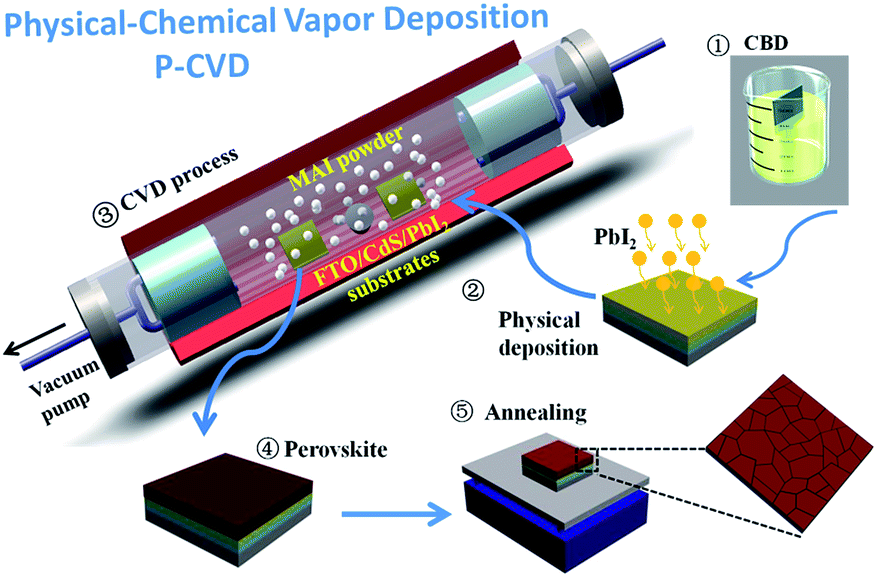 | ||
| Fig. 1 Schematic diagram of CdS-based PSCs deposited by physical–chemical vapor deposition (P-CVD) process. | ||
Device fabrication
The FTO glasses and PET/ITO flexible substrates (with the size of 30 × 30 mm) were washed with soap, acetone, ethanol and deionized water using ultrasonication, respectively. After the CdS film formed on the FTO substrates, the perovskite absorption layer was deposited by the P-CVD process. The hole transfer layer was deposited above the perovskite film by spin-coated the Spiro-OMeTAD solution (72.3 mg Spiro-OMeTAD dissolved in the 1 mL of chlorobenzene with the 28.8 μL of 4-tert-butylpyridine and 17.5 μL of lithium bis(trifluoromethanesulfonyl)imide solution) at 3500 rpm, 30 s. Finally, the 120 nm thickness of silver electrode was deposited on the HTM by thermal evaporation with the active area of 0.09 cm2.Characterization
The morphologies of the perovskite and CdS thin film was analyzed by the field emission scanning electron microscopy (FE-SEM, Sigma Zeiss) and the crystal phase of perovskite and CdS were identified by X-ray powder diffraction (XRD) utilizing a Cu Kα radiation, and composition of CdS based perovskite was analyzed by X-ray photoelectron spectra (XPS, Thermo ESCALAB 250). The absorption spectrum of perovskite film and transmission spectra of CdS films were measured by UV-visible spectrophotometer (UV-2550) and a Hitachi F-4600 fluorescence spectrophotometer, respectively. The thickness of the CdS film was performed by ellipsometer (SE400). Photocurrent density–voltage (J–V) measurements were conducted using a Keithley 2636 system sourcemeter and a Xenon Lamp Solar Simulator Equipped with an AM 1.5 irradiation (∼100 mW cm−2). The incident photon-to-current conversion efficiency (IPCE) was tested using Zolix spectrograph, where illumination was provided by a Xenon lamp, with standard silicon cell as reference. The bending test of the devices was performed as a function of the number of bending cycles in an outward direction at a bending radius of ∼8 mm.Results and discussion
Fig. 2d shows the X-ray diffraction (XRD) patterns of CdS, PbI2 and perovskite thin film on the FTO substrates. The diffraction peak at 2θ = 27° of CdS is attributed to the CdS hexagonal structure of (002), while the diffraction peaks at 12.62° of (001), 38.54° of (003), and 52.30° of (004) to PbI2 with the hexagonal structure. Moreover, the typical perovskite (CH3NH3PbI3) peak is found at 14.07° of (110), and other peaks at 28.36°, 31.82°, 43.14° to the (220), (310), and (330) planes, respectively. Meanwhile, the absorption spectrum of the perovskite film, presented in the Fig. 2e, exhibits a wide absorption spectrum from 300–800 nm, which is beneficial for achieving a strong absorption of light for photovoltaic applications.45 | ||
| Fig. 2 The SEM morphologies of (a) CdS thin film, (b) PbI2 thin film on the FTO/CdS substrate. (c) Low- and high-magnification of the CH3NH3PbI3 film on the FTO/CdS substrate after annealing. (d) The X-ray diffraction patterns of FTO (black line), FTO/CdS (pink line), FTO/CdS/PbI2 (red line) and FTO/CdS/CH3NH3PbI3 (blue line). (e) The absorption spectrum of CH3NH3PbI3 film (the photograph of perovskite film shown in inset). | ||
Furthermore, the morphologies of CdS, PbI2 and perovskite films are investigated after annealing. As shown in Fig. 2a, the CdS film is rather uniform and compact upon the FTO substrate without any discernible pinholes. This is beneficial for the subsequent PbI2 and perovskite film deposition, and will help to promote electrons transport. Importantly, the full and compact coverage by the CdS layer can effectively block the recombination of the electrons and holes at the interface of the FTO/perovskite and reduce the leakage. Fig. 2b and S1† show the morphologies of nano-crystalline PbI2 with grain sizes of 200–300 nm, which can facilitate the MAI vapour to immerse into the film and promote a full conversion of the PbI2 layer into perovskite. After reaction and annealing at 100 °C, the SEM image of the perovskite film with large grains on the substrates are shown in Fig. S2.† The morphology change during the reaction process could be assigned to the expansion and re-construction of the hexagonal PbI2 structure into the orthorhombic perovskite structure.17,45,46 What's more, a typical cross-section SEM image (Fig. 2e) exhibits a uniform and full coverage of the perovskite film, with an average thickness of ∼350 ± 50 nm, upon the FTO/CdS substrates. To investigate the morphology of perovskite thin film, the surface topography of the perovskite film is characterized by using atomic force microscope (AFM). Fig. S3 and S4† present the AFM images of the CdS and perovskite film over an area of 2 μm × 2 μm and 5 μm × 5 μm, respectively. We find that the CBD-processed CdS film is rather uniform and smooth with a roughness of ∼10.5 nm without post annealing, and the perovskite film also an exhibits excellent thin film uniformity with a lower roughness of ∼20 nm, which is an important guarantee to prevent the formation of electric leakage path in PSCs, a prerequisite for high efficient solar cells.
Fig. 3a and b show the device structure and the band gap profile/levels of the CdS based PSCs. In this configuration, CdS features a broad-band gap ∼2.4 eV and a conduction band edge lying 0.3 eV lower than that of perovskite, which can rapidly extract electrons to the cathode and effectively block the holes injection at the CdS/perovskite interface. Then, we proceed to fabricate CdS-based perovskite solar cell devices with a configuration of FTO/CdS/perovskite/Spiro-OMeTAD/Ag. Fig. 3d shows the photocurrent density–voltage (J–V) curves of the CdS-based PSCs, with 5 different CdS layer thicknesses from 30 nm to 120 nm, while their photovoltaic parameters are summarized in Table 1. When the CdS is too thin of only 30 nm, the PSC shows a poor contact and low fill factor (FF), and the increasing of the CdS thickness to 50 nm helps to improve the overall performance with a higher FF factor to 0.65. However, further increasing of the thickness of CdS film leads to a significantly drop in Jsc from 20.67 mA cm−2 to 17.06 mA cm−2 and lower Voc and FF. The performance deterioration can be attributed to the increasing absorption loses and higher series resistance (Rs) in the thickening ETL CdS layer. This can also be inferred from the transmission spectra of the CdS layers presented in Fig. 3c, where for the incident wavelengths from 300 nm to 520 nm, a thicker CdS film causes a stronger absorption that will reduce the effective light harvesting in the active perovskite layer. Therefore, as a trade-off, an optimum CdS film thickness is found to be ∼50 nm (corresponding to 6 min deposition), which exhibits a high PCE of 13.3% with Voc = 0.99 V, Jsc = 20.65 mA cm−2, and FF = 0.65, respectively.
 | ||
| Fig. 3 (a) Device structure of the CdS based planar PSCs. (b) Energy level of CdS based PSCs. (c) The transparent spectra of CdS with different thickness by CBD (CdS thin film on the FTO shown in the inset photograph). (d) J–V characteristics of CH3NH3PbI3 deposited on FTO/CdS substrates with various thickness of CdS thin film. | ||
| Time (min) | Thickness (nm) | Voc (V) | Jsc (mA cm−2) | FF | PCE (%) | Rs (Ωcm2) | Rsh (Ωcm2) |
|---|---|---|---|---|---|---|---|
| 5 | 30 | 0.96 | 20.41 | 0.45 | 8.92 | 16.5 | 258.8 |
| 6 | 50 | 0.99 | 20.67 | 0.65 | 13.30 | 8.6 | 775.2 |
| 8 | 70 | 0.97 | 20.38 | 0.63 | 12.46 | 13.9 | 712.4 |
| 10 | 100 | 0.91 | 19.37 | 0.55 | 9.77 | 11.7 | 589.6 |
| 12 | 120 | 0.93 | 17.06 | 0.54 | 8.76 | 12.9 | 267.7 |
Meanwhile, it is also important to note that, the reaction temperature of PbI2 and MAI in the CVD process plays a key role, to some extent, in promoting an in situ Cd-doping into the as-produced perovskite film. As witnessed from the XPS spectra of the perovskite film prepared upon CdS thin film, shown in Fig. 4a–c, the peak at ∼404 eV indicates that Cd has diffused into the perovskite thin film as impurity.44 And the two overlapping components of Pb 4d5/2 and Cd 3d3/2 at 412 eV is asymmetrical, which suggests that it is formed by several contributions.47 Importantly, the sulfide is not detected in the film, which indicates that the Cd signal does not come from the underlying CdS layer, but from the diffused Cd into the perovskite film. The J–V curves of such Cd-doped PSCs, deposited at different reaction temperatures ranging from 100 to 130 °C, are displayed in Fig. 4d, where we found that the PSC prepared at 110 °C achieves the highest PCE of 13.3%. This improvement can be attributed to the fact that an in situ Cd-doping during the CVD process that can effectively lower the conduction band edge of perovskite to facilitate electron extraction. However, if the deposition temperature is too low (to 100 °C), the remnant PbI2 may not be fully converted into perovskite,48 and thus impedes photocurrent extraction as PbI2 by itself has a wider bandgap than that of perovskite. But, if an excess amount of Cd is injected into the perovskite thin film,44 happened at higher temperature, the perovskite will become instable and decompose in a series of three-steps reaction as detailed below.44,47,49
| CH3NH3PbI3 + CdS → CH3NH3I + PbI2 + CdS |
| CH3NH3I → CH2NH2 + HI |
| CdS + 2HI → CdI2 + H2S |
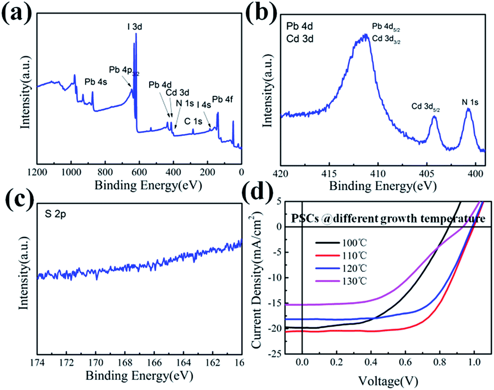 | ||
| Fig. 4 The XPS spectra for (a) perovskite film, (b) Cd 3d, (c) S 2p, (d) the PCE of CdS based (CH3NH3PbI3) PSCs on different deposition temperature. | ||
The highest PCE of CdS-based PSC presented in Fig. 5a is up to 14.68% with the Voc of 1.04 V, Jsc of 20.76 mA cm−2 and FF of 0.68. The incident photon-to-current conversion efficiency (IPCE) spectrum is shown in Fig. 5b. The maximum IPCE of PSCs reaches over 80% and the integrated current density is estimated to 18.1 mA cm−2, which is lower than the Jsc from the J–V curve. In order to further understand the performance of CdS based PSCs, the typical J–V curves under forward and reverse scan for the CdS based PSCs are shown in Fig. 5a. The CdS based PSC presents a high PCE of 13.15% with the Voc = 1.02 V, Jsc = 19.53 mA cm−2, and FF = 0.66 under forward scanning, which exhibit a little hysteresis in the device, suggesting that CdS film can alleviate the hysteresis effects, which will be beneficial to its widely application. In addition, the stability is also an important aspect for PSCs. For the CdS-based PSCs, there is no report about the stability of the device in previous work. And our process provided the stability for the devices for the first time without particular encapsulation (seen in Fig. S5†). The device still maintained 11.48% after storing in the air for 72 h. However, the performance of the devices dropped significantly due to the Spiro-OMeTAD inevitably contacted with moisture in the air. But the devices still maintain 30% of the initial efficiencies after 480 h.
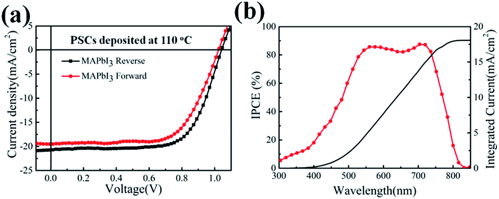 | ||
| Fig. 5 (a) The J–V curves of the best CdS based PSCs. (b) The IPCE spectra of best CdS based PSCs. | ||
Table 2 shows a comparison of our CdS-based PSCs prepared via a P-CVD to others CdS-based PSCs in the literature. Comparing to the traditional solution methods, the advantage of the P-CVD process could be summarized as (i) first, the in situ growth of a compact perovskite thin film upon CdS ETL layers, via P-CVD process, can effectively reduce the surface roughness, the interface defect and suppress the leakage pinholes, which is critical to achieve to a high photocurrent output; (ii) second, the CdS deposited on the FTO substrates interface can also suppress the activation of intrinsic trap sites originating from the FTO film, as there is no oxygen vacancy in the CdS film, which can help to reduce the charge-trapping between the perovskite and the ETL layers.50 (iii) Third, during the MAI deposition process in furnace, there is also an annealing process for CdS thin film, which can promote the CdS grains to grow and merge into a compact thin film with higher density and better conductivity; (iv) the P-CVD procedure relies on a vacuum system to form perovskite film without extra solvent. This can prevent the DMF, DMSO and GBL solvent inclusion that may damage the film quality, and ensure a better crystallization of the forming perovskite grains and eliminate metastable phase in the thin film.17,51
| Device | Method | Voc (V) | Jsc (mA cm−2) | FF | PCE (%) | Ref. |
|---|---|---|---|---|---|---|
| FTO/CdS/MAPbI3/Spiro-OMeTAD/Ag | P-CVD | 1.04 | 20.76 | 0.68 | 14.68 | Our work |
| PET/ITO/CdS/MAPbI3/Spiro-OMeTAD/Ag | P-CVD | 0.94 | 17.65 | 0.6 | 9.93 | Our work |
| FTO/CdS/MAPbI3 Spiro-OMeTAD/Au | Solution | 1.05 | 16.14 | 0.66 | 11.17 | 43 |
| FTO/CdS/MAPbI3/Spiro-OMeTAD/Ag | Solution | 0.98 | 17.54 | 0.71 | 12.2 | 50 |
| FTO/m-TiO2/CdS/MAPbI3/Spiro-OMeTAD/Au | Solution | 0.93 | 17.6 | 0.7 | 11.46 | 54 |
| FTO/CdS/MAPbI3/Spiro-OMeTAD/Ag | Solution | 1.05 | 20.6 | 0.7 | 15.1 | 44 |
| FTO/CdS/PbSQDs/MoO3/Ag | Solution | 0.46 | 24.8 | 0.47 | 5.22 | 55 |
| ITO/CdS NRs/MAPbI3 Spiro-OMeTAD/MoO3/Ag | Solution | 0.89 | 18.77 | 0.499 | 8.36 | 56 |
| FTO/CdS NRs/PbSQDs/MoO3/Ag | Solution | 0.51 | 23.00 | 0.42 | 4.78 | 57 |
As the CdS thin film can be deposited in chemical bath deposition at very low temperature without the need of high temperature annealing, the CdS-based PSCs can be prepared directly upon flexible and large plastic substrates (PET). In a context of rapidly growing research interests in high performance flexible PSC applications,30 we develop a flexible perovskite solar cell with the CdS as ETL via P-CVD procedure on flexible PET/ITO substrates. The CdS electron transfer layer is deposited via CBD at 80 °C, while the perovskite is formed by P-CVD process also in a relative lower temperature at 110 °C (see in Fig. S6†), with a configuration as illustrated in Fig. 6a.
 | ||
| Fig. 6 (a) The device structure of the CdS based perovskite planar flexible solar cells. (b) J–V characteristics of CdS based perovskite flexible solar cells. (c) The IPCE spectrum of CdS based perovskite flexible solar cells. (d) Normalized value as a function of number of bending cycles. | ||
The J–V curve in Fig. 6b shows that the flexible perovskite solar cell can achieve a high PCE of 9.93% with a reasonable Voc = 0.94 V, Jsc = 17.65 mA cm−2 and FF = 0.6, respectively. The IPCE of the flexible PSC device (with 50 nm thick CdS layer) is measured and shown in Fig. 6c, which exhibits a broad peak over the spectrum range of 300–800 nm. The solar spectrum weighted integral of the IPCE response is also calculated to obtain a photocurrent density Jsc of 16.5 mA cm−2, which agrees well with that determined by direct J–V measurement. Besides, in order to testify the mechanical stability of the flexible perovskite solar cell device, the J–V curves recorded after repeated bending testing to a small radius of 8 mm up to 100 cycles are shown in Fig. 6d. It is interesting to find that the PSC devices can maintain 49% of its initial efficiency after 100 bending cycles, highlighting the potential of low-temperature P-CVD fabricated CdS-based PSCs for high performance, low-cost and durable flexible photovoltaics. It is important to note that, though the performance of our flexible PSC devices is not as good as those flexible perovskite solar cells based on organic or TiO2, ZnO,30,52,53 the very low cost and low-temperature-processed (<85 °C) CdS ETL layer technology, as well as a facile fabrication procedure, represent indeed very critical aspects for large scale implementation of the cost-sensitive flexible solar cell applications. And there is still plenty of room for improvement given further structural and compositional optimization of this new fabrication strategy in future works.
Conclusions
In summary, we have reported a new flexible perovskite solar cell fabrication, with low-temperature-processed CdS thin film as electron transfer layer and via a P-CVD procedure. A parametric optimization of the CdS layer thickness and an advantageous in situ Cd-doping of the perovskite thin film leads to a high PCE of ∼14.68% with the Voc of 1.04 V, the Jsc of 20.76 mA cm−2, and the FF of 0.68 on solid substrate. Furthermore, this lower temperature (<85 °C) procedure also enables us to implement a flexible perovskite solar cells directly upon plastic PET substrate, where a high PCE of 9.9% has been demonstrated, for the first time, for the CdS-based PSC devices. These promising results indicate that the inorganic sulfur compound can serve as an ideal low-cost alternative electron transfer layer material, with an important potential to implement a large-area and low-temperature fabrication of high performance flexible photovoltaics.Acknowledgements
This work was financed by Scientific and Technological Support Programme in Jiangsu province under No. BE2014147-2, NSFC under No. 61674075, 11274155, 61204050, U1632151, Open Research Fund of State Key Laboratory of Pulsed Power Laser Technology of China (Hefei, SKL 2015 KF 04), JSNSFC No. BK20150275, Jiangsu Shuangchuang Team's and Personal Program, Jiangsu Excellent Young Scholar Program and the Fundamental Research Funds for the Central Universities.Notes and references
- H. Lu, W. Tian, F. Cao, Y. Ma, B. Gu and L. Li, Adv. Funct. Mater., 2016, 26, 1296–1302 CrossRef CAS.
- S. Kazim, M. K. Nazeeruddin, M. Grätzel and S. Ahmad, Angew. Chem., Int. Ed., 2014, 53, 2812–2824 CrossRef CAS PubMed.
- M. A. Green, A. Ho-Baillie and H. J. Snaith, Nat. Photonics, 2014, 8, 506–514 CrossRef CAS.
- Y. Fang and J. Huang, Adv. Mater., 2015, 27, 2804–2810 CrossRef CAS PubMed.
- L. Dou, Y. M. Yang, J. You, Z. Hong, W. H. Chang, G. Li and Y. Yang, Nat. Commun., 2014, 5, 5404 CrossRef CAS PubMed.
- Z. K. Tan, R. S. Moghaddam, M. L. Lai, P. Docampo, R. Higler, F. Deschler, M. Price, A. Sadhanala, L. M. Pazos, D. Credgington, F. Hanusch, T. Bein, H. J. Snaith and R. H. Friend, Nat. Nanotechnol., 2014, 9, 687–692 CrossRef CAS PubMed.
- O. A. Jaramillo-Quintero, R. S. Sanchez, M. Rincon and I. Mora-Sero, J. Phys. Chem. Lett., 2015, 6, 1883–1890 CrossRef CAS PubMed.
- Q. Zhang, S. T. Ha, X. Liu, T. C. Sum and Q. Xiong, Nano Lett., 2014, 14, 5995–6001 CrossRef CAS PubMed.
- Y. Zhao and K. Zhu, Chem. Soc. Rev., 2016, 45, 655–689 RSC.
- K. T. Akihiro Kojima, Y. Shirai and T. Miyasaka, J. Am. Chem. Soc., 2009, 131, 6050–6051 CrossRef PubMed.
- C. Yi, X. Li, J. Luo, S. M. Zakeeruddin and M. Gratzel, Adv. Mater., 2016, 28, 2964–2970 CrossRef CAS PubMed.
- F. Wang, W. Geng, Y. Zhou, H. H. Fang, C. J. Tong, M. A. Loi, L. M. Liu and N. Zhao, Adv. Mater., 2016, 28, 9986–9992 CrossRef CAS PubMed.
- M. Liu, M. B. Johnston and H. J. Snaith, Nature, 2013, 501, 395–398 CrossRef CAS PubMed.
- M. M. Tavakoli, L. Gu, Y. Gao, C. Reckmeier, J. He, A. L. Rogach, Y. Yao and Z. Fan, Sci. Rep., 2015, 5, 14083 CrossRef PubMed.
- C. Gao, J. Liu, C. Liao, Q. Ye, Y. Zhang, X. He, X. Guo, J. Mei and W. Lau, RSC Adv., 2015, 5, 26175–26180 RSC.
- J. Mao, H. Zhang, H. He, H. Lu, F. Xie, D. Zhang, K. S. Wong and W. C. H. Choy, RSC Adv., 2015, 5, 73760–73766 RSC.
- Q. Chen, H. Zhou, Z. Hong, S. Luo, H. S. Duan, H. H. Wang, Y. Liu, G. Li and Y. Yang, J. Am. Chem. Soc., 2014, 136, 622–625 CrossRef CAS PubMed.
- R. Sheng, A. Ho-Baillie, S. Huang, S. Chen, X. Wen, X. Hao and M. A. Green, J. Phys. Chem. C, 2015, 119, 3545–3549 CAS.
- B. S. Tosun and H. W. Hillhouse, J. Phys. Chem. Lett., 2015, 6, 2503–2508 CrossRef CAS PubMed.
- A. Ng, Z. Ren, Q. Shen, S. H. Cheung, H. C. Gokkaya, S. K. So, A. B. Djurisic, Y. Wan, X. Wu and C. Surya, ACS Appl. Mater. Interfaces, 2016, 8, 32805–32814 CAS.
- Y. Peng, G. Jing and T. Cui, J. Mater. Chem. A, 2015, 3, 12436–12442 CAS.
- Y. Peng, G. Jing and T. Cui, RSC Adv., 2015, 5, 95847–95853 RSC.
- Y. Li, J. K. Cooper, R. Buonsanti, C. Giannini, Y. Liu, F. M. Toma and I. D. Sharp, J. Phys. Chem. Lett., 2015, 6, 493–499 CrossRef CAS PubMed.
- C. Liu, K. Wang, C. Yi, X. Shi, A. W. Smith, X. Gong and A. J. Heeger, Adv. Funct. Mater., 2016, 26, 101–110 CrossRef CAS.
- Y. Wang, S. Li, P. Zhang, D. Liu, X. Gu, H. Sarvari, Z. Ye, J. Wu, Z. Wang and Z. D. Chen, Nanoscale, 2016, 8, 19654–19661 RSC.
- J. Troughton, M. J. Carnie, M. L. Davies, C. Charbonneau, E. H. Jewell, D. A. Worsley and T. M. Watson, J. Mater. Chem. A, 2016, 4, 3471–3476 CAS.
- D. B. W. Tress, M. I. Dar, P. Gao, J. Luo, C. Renevier, K. Schenk, A. Abate, F. Giordano, J. P. Correa Baena, J. D. Decoppet, S. M. Zakeeruddin, M. K. Nazeeruddin, M. Grätzel and A. Hagfeldt, Sci. Adv., 2016, 2, 1501170 Search PubMed.
- National Renewable Energy Laboratory, Best Research Cell Efficiency, http://www.nrel.gov/ncpv/images/efficiency_chart.jpg, accessed, January, 2016.
- O. Malinkiewicz, A. Yella, Y. H. Lee, G. M. Espallargas, M. Graetzel, M. K. Nazeeruddin and H. J. Bolink, Nat. Photonics, 2014, 8, 128–132 CrossRef CAS.
- D. Liu and T. L. Kelly, Nat. Photonics, 2013, 8, 133–138 CrossRef.
- Y. Lin, J. Wang, Z. G. Zhang, H. Bai, Y. Li, D. Zhu and X. Zhan, Adv. Mater., 2015, 27, 1170–1174 CrossRef CAS PubMed.
- Y. Lin, F. Zhao, Q. He, L. Huo, Y. Wu, T. C. Parker, W. Ma, Y. Sun, C. Wang, D. Zhu, A. J. Heeger, S. R. Marder and X. Zhan, J. Am. Chem. Soc., 2016, 138, 4955–4961 CrossRef CAS PubMed.
- Z. L. Tseng, C. H. Chiang and C. G. Wu, Sci. Rep., 2015, 5, 13211 CrossRef CAS PubMed.
- K. Wojciechowski, T. Leijtens, S. Siprova, C. Schlueter, M. T. Horantner, J. T. Wang, C. Z. Li, A. K. Jen, T. L. Lee and H. J. Snaith, J. Phys. Chem. Lett., 2015, 6, 2399–2405 CrossRef CAS PubMed.
- X. Wang, L.-L. Deng, L.-Y. Wang, S.-M. Dai, Z. Xing, X.-X. Zhan, X.-Z. Lu, S.-Y. Xie, R.-B. Huang and L.-S. Zheng, J. Mater. Chem. A, 2017, 5, 1706–1712 CAS.
- W. Ke, G. Fang, Q. Liu, L. Xiong, P. Qin, H. Tao, J. Wang, H. Lei, B. Li, J. Wan, G. Yang and Y. Yan, J. Am. Chem. Soc., 2015, 137, 6730–6733 CrossRef CAS PubMed.
- K. Wang, Y. Shi, Q. Dong, Y. Li, S. Wang, X. Yu, M. Wu and T. Ma, J. Phys. Chem. Lett., 2015, 6, 755–759 CrossRef CAS PubMed.
- M. Qin, J. Ma, W. Ke, P. Qin, H. Lei, H. Tao, X. Zheng, L. Xiong, Q. Liu, Z. Chen, J. Lu, G. Yang and G. Fang, ACS Appl. Mater. Interfaces, 2016, 8, 8460–8466 CAS.
- B. L. Williams, J. D. Major, L. Bowen, L. Phillips, G. Zoppi, I. Forbes and K. Durose, Sol. Energy Mater. Sol. Cells, 2014, 124, 31–38 CrossRef CAS.
- A. Morales-Acevedo, Sol. Energy Mater. Sol. Cells, 2006, 90, 2213–2220 CrossRef CAS.
- K. Ramanathan, M. A. Contreras, C. L. Perkins, S. Asher, F. S. Hasoon, J. Keane, D. Young, M. Romero, W. Metzger, R. Noufi, J. Ward and A. Duda, Progress in Photovoltaics: Research and Applications, 2003, 11, 225–230 CrossRef CAS.
- S. Lee, E. S. Lee, T. Y. Kim, J. S. Cho, Y. J. Eo, J. H. Yun and A. Cho, Sol. Energy Mater. Sol. Cells, 2015, 141, 299–308 CrossRef CAS.
- J. Liu, C. Gao, L. Luo, Q. Ye, X. He, L. Ouyang, X. Guo, D. Zhuang, C. Liao, J. Mei and W. Lau, J. Mater. Chem. A, 2015, 3, 11750–11755 CAS.
- W. A. Dunlap-Shohl, R. Younts, B. Gautam, K. Gundogdu and D. B. Mitzi, J. Phys. Chem. C, 2016, 120, 16437–16445 CAS.
- M. R. Leyden, L. K. Ono, S. R. Raga, Y. Kato, S. Wang and Y. Qi, J. Mater. Chem. A, 2014, 2, 18742–18745 CAS.
- Q. Guo, C. Li, W. Qiao, S. Ma, F. Wang, B. Zhang, L. Hu, S. Dai and Z. A. Tan, Energy Environ. Sci., 2016, 9, 1486–1494 CAS.
- J. Navas, A. Sanchez-Coronilla, J. J. Gallardo, N. C. Hernandez, J. C. Pinero, R. Alcantara, C. Fernandez-Lorenzo, D. M. De los Santos, T. Aguilar and J. Martin-Calleja, Nanoscale, 2015, 7, 6216–6229 RSC.
- C. W. Chen, H. W. Kang, S. Y. Hsiao, P. F. Yang, K. M. Chiang and H. W. Lin, Adv. Mater., 2014, 26, 6647–6652 CrossRef CAS PubMed.
- J. Navas, A. Sanchez-Coronilla, J. J. Gallardo, E. I. Martin, N. C. Hernandez, R. Alcantara, C. Fernandez-Lorenzo and J. Martin-Calleja, Phys. Chem. Chem. Phys., 2015, 17, 23886–23896 RSC.
- I. Hwang and K. Yong, ACS Appl. Mater. Interfaces, 2016, 8, 4226–4232 CAS.
- X. Li, D. Bi, C. Yi, J.-D. Décoppet, J. Luo, S. M. Zakeeruddin, A. Hagfeldt and M. Grätzel, Science, 2016, 353, 58–62 CrossRef CAS PubMed.
- S. Ryu, J. Seo, S. S. Shin, Y. C. Kim, N. J. Jeon, J. H. Noh and S. I. Seok, J. Mater. Chem. A, 2015, 3, 3271–3275 CAS.
- L. Chen, F. Tang, Y. Wang, S. Gao, W. Cao, J. Cai and L. Chen, Nano Res., 2015, 8, 263–270 CrossRef CAS.
- I. Hwang, M. Baek and K. Yong, ACS Appl. Mater. Interfaces, 2015, 7, 27863–27870 CAS.
- X. Yao, Y. Chang, G. Li, L. Mi, S. Liu, H. Wang, Y. Yu and Y. Jiang, Sol. Energy Mater. Sol. Cells, 2015, 137, 287–292 CrossRef CAS.
- Z. Gu, F. Chen, X. Zhang, Y. Liu, C. Fan, G. Wu, H. Li and H. Chen, Sol. Energy Mater. Sol. Cells, 2015, 140, 396–404 CrossRef CAS.
- X. Yao, S. Liu, Y. Chang, G. Li, L. Mi, X. Wang and Y. Jiang, ACS Appl. Mater. Interfaces, 2015, 7, 23117–23123 CAS.
Footnote |
| † Electronic supplementary information (ESI) available. See DOI: 10.1039/c7ra01110e |
| This journal is © The Royal Society of Chemistry 2017 |