
 Open Access Article
 This Open Access Article is licensed under a
 Creative Commons Attribution 3.0 Unported Licence
Copper–gold sandwich structures on PE and PET and their SERS enhancement effect
Alena Reznickova *a,
Petr Slepickaa,
Hoang Yen Nguyenovaa,
Zdenka Kolskab,
Marcela Dendisovac and
Vaclav Svorcika
*a,
Petr Slepickaa,
Hoang Yen Nguyenovaa,
Zdenka Kolskab,
Marcela Dendisovac and
Vaclav Svorcika
aDepartment of Solid State Engineering, University of Chemistry and Technology Prague, 166 28 Prague 6, Czech Republic. E-mail: reznicka@vscht.cz
bFaculty of Science, J. E. Purkyne University, 400 96 Usti nad Labem, Czech Republic
cDepartment of Physical Chemistry, University of Chemistry and Technology Prague, 166 28 Prague 6, Czech Republic
First published on 26th April 2017
Abstract
A Surface Enhanced Raman Spectroscopy (SERS) system with the coupling between surface plasmon polaritons (SPPs) supported by a gold grating and localized surface plasmons (LSPs) excited on grafted copper nanoparticles (CuNPs) was designed and characterized. The excitation of copper nanoparticles–molecules–gold layer sandwich structures was studied under 633 nm wavelength irradiation. Rhodamine 6G (R6G) molecules were added onto SERS substrates and located above and between the CuNPs. Prepared samples were studied by several experimental techniques: goniometry, X-ray photoelectron spectroscopy (XPS), energy dispersive X-ray spectroscopy (EDS), scanning electron microscopy (SEM), atomic force microscopy (AFM) and electrokinetic analysis. Aging of the modified PE and PET was accompanied by an increase in the contact angle, which was due to a reorientation of the molecular polar segments produced during the plasma treatment. XPS and zeta potential measurements indicated that the thiols were chemically bonded to the gold coated polymer surfaces and that the thiols mediate subsequent grafting of Cu nanoparticles. Both XPS and EDS analyses revealed that a higher concentration of grafted copper nanoparticles was achieved on the PET substrate. EDS showed that Cu nanoparticles are homogeneously distributed over the whole polymer surface. The enhancement factor was higher for PE (1.7 × 10³) compared to PET (0.9 × 10²).
1. Introduction
Surface Enhanced Raman Spectroscopy (SERS) is an important analytical technique that is able to provide single molecule detection and high-resolution spectral information. It has been widely accepted that there are two separate mechanisms to describe the overall SERS effect: the electromagnetic effect (EM) and the chemical mechanism (CM). The EM mechanism is based on the interaction of the transition moment of an adsorbed molecule with the electric field of a surface plasmon induced by the incoming light at the metal, whereas the CM is based on the interaction of the adsorbate adsorbed on the metal and the metal itself, mostly from the first layer of the charge-transfer resonance between the adsorbate and the metal.1Recent studies on single molecule detection by SERS indicate that a large enhancement of the order of 1014 to 1015 can be obtained at the junctions of two aggregated nanoparticles (NPs) due to the coupling of the localized surface plasmon (LSP) of the metal NPs produced by hot spots.2,3 The coupling effect has been documented by research on a surface plasmon resonance (SPR) device, as reported by Hutter et al.4 They have systematically studied the enhancement effect of the metal NPs on the SPR of the gold and silver film and attributed the enhancement to the coupling of the LSP-SPP. Later, Orendorff et al. fabricated a sandwich architecture of smooth gold–molecules–gold nanoparticles with different shapes with which high enhancement factors (EFs) in the range of 107 and 109 were obtained and attributed to LSP-SPP coupling.5 However, all these studies are on the LSP-SPP coupling of the same metals. Most recently, Kim et al. have investigated the coupling of silver–gold, silver–copper, and gold–copper by fabricating junctions on the gold and copper substrates.6 It was found that silver–copper coupling is more effective than that of gold–copper in visible light. Daniels et al. have fabricated a silver nanoparticles–molecules–silver mirror sandwich structure for SERS and found that the enhancement in Raman scattering in the sandwich structure is larger than that on a roughened silver surface due to the plasmon coupling between the particles themselves as well as the coupling between the particles and the underlying continuous film.3,7
Many different types of SERS substrates, which meet the above requirements have been developed, including roughened electrodes, noble metal colloidal nanoparticles,8 silver island films,9,10 metal film over nanostructured surfaces,11 acid-etched metal foils, and lithographically produced nanoparticle arrays.12 Plastic substrates are also known.13 Polymers were commonly used for improved mechanical stability of nanoparticles14 and better signal reproducibility via embossing surfaces and lithographic techniques.15
Polyethylene (PE) and polyethyleneterephthalate (PET) are polymers with broad potential applications in microelectronics. PE and PET foils, for example, after plasma treatment have great surface roughness with improved adhesive properties for sputtering a gold overlayer and can be positive for an electromagnetic mechanism. A gold overlayer can suppress the Raman background signal of the polymer substrate.13,16
In this paper we have investigated the SERS effect of gold–copper sandwich structures (i.e. the coupling between surface plasmon polaritons (SPPs) supported by the gold grating and localized surface plasmons (LSPs) excited on the grafted copper nanoparticles (CuNPs)7,17,18) with the aim to gradually cover LSP excitation in the 500–850 nm wavelength range. The enhancement with copper nanoparticles–molecules–gold layer sandwich structures is studied under 633 nm wavelength illumination. Rhodamine 6G (R6G) molecules are added onto SERS substrates and located above and between the CuNPs. The surface properties of pristine PE and PET and their modified counterparts were studied by different experimental techniques: goniometry, X-ray photoelectron spectroscopy (XPS), energy dispersive X-ray spectroscopy (EDS) and electrokinetic analysis to determine the surface wettability, polarity and chemistry of the modified polymer, respectively. Sample surface evaluation after each step of the preparation procedure was checked by AFM and SEM microscopy, respectively. The studied systems could be helpful not only for theoretical research into the LSP-SPP effect by SERS but the metal-to-metal junctions also have great applications in molecular electronic devices and biology.19,20
2. Experimental
2.1 Materials and sample preparation
Biaxially oriented polyethyleneterephthalate (PET, density 1.3 g cm−3, Mw = 4 × 10³ g mol−1, 23 μm foil, supplied by Goodfellow Ltd., UK) and high density polyethylene (HDPE, 0.95 g cm−3, Mw = 4 × 10⁵ g mol−1, 40 μm foil, supplied by Granitol Ltd., CZ) were used in this study. These substrates were chosen as representatives of polar and nonpolar polymers.In the 1st step, samples were treated in Ar+ plasma on a Balzers SCD 050 device (Pfaeffikon Balzers, Liechtenstein): exposure time 120 s, discharge power 8.3 W, gas purity 99.996% (supplied by Siad Ltd., Czech Republic), flow rate 0.3 l s−1, pressure 10 Pa, electrode distance 50 mm and electrode area 48 cm2, chamber volume approx. 1000 cm3, plasma volume 240 cm3. Treatment was accomplished at laboratory temperature. In the 2nd step, treated polymer foil was deposited with a layer of gold. Gold was deposited onto a patterned surface by vacuum sputtering (DC Ar plasma, gas purity 99.996%, gas pressure 4 Pa, discharge current 40 mA and sputtering time 150 s). We prepared an 80 nm (which is in the middle of the interval) thick Au layer because it is well known that the surface roughness on a 50–200 nm scale is crucial for exhibiting a large EF.6,7 The deposition of gold was accomplished from an Au target (purity 99.99%, provided by Safina Ltd., CZ). In the 3rd step, plasma treated foil with a gold layer was grafted by biphenyl-4,4′-dithiol (BPD; 1 × 10⁻⁴ mol l−1; grafting time 24 h; Sigma-Aldrich Corp.; US) and a BPD monolayer assembled on an Au layer was created.6,18 In the 4th step, such a modified foil was placed into an aqueous solution of CuNPs for 2 h. The colloidal solution of CuNPs had the following properties: average size (12.2 ± 5.2) nm and concentration of Cu in the colloidal solution 5.3 × 10⁻⁴ mol l−1.21 A more detailed description of the CuNPs preparation can be found in (ref. 22). After that the foil was removed from the solution, washed by methanol (purity p.a., Penta Ltd., Czech Republic) and dried in the air.
2.2 Measurement and techniques
Ultraviolet-visible (UV-Vis) absorption spectra were recorded using a Lambda 25 UV-Vis spectrophotometer (PerkinElmer Inc., US). The colloidal solutions of CuNPs were kept in a 1 cm quartz cell. The reference spectrum of the solvent (water) was subtracted from the spectra of the colloidal solutions of CuNPs. Data were collected from 200 to 700 nm with a 1 nm data step at a scan rate of 240 nm min−1.Detailed structural characterization of copper nanoparticles was performed using a high resolution transmission electron microscope (HRTEM, JEOL JEM-2200FS, JEOL Ltd., Tokyo, Japan) operated at 200 kV.
Water contact angles (WCA) of distilled water, characterizing the structural and compositional changes caused by the plasma treatment, were measured at room temperature on two samples at seven positions each, using a drop shape analyzer (DSA 100, KRÜSS GmbH, DE). Drops of (2.0 ± 0.2) μl of water were deposited on the test samples using an automatic pipette. Images of the drops were taken after a 2 s delay. Contact angles were then evaluated using DSA4 software. In this experiment, the contact angles on the plasma treated samples were measured immediately after the modification and then after 15 and 45 min, 1, 3 and 6 h, 1 day, 3, 7, 14, and 30 days after modification.
Concentrations of C(1s), O(1s), Au(4f), S(2p) and Cu(2p3/2) atoms in the modified surface layer were measured by X-ray Photoelectron Spectroscopy (XPS). An Omicron Nanotechnology ESCAProbe P spectrometer (Omicron Nanotechnology GmbH, DE) was used to measure the photoelectron spectra (typical error of 5%). XPS analysis was performed at a pressure of 2 × 10⁻⁸ Pa. The exposed and analyzed area had dimensions of 2 × 3 mm2. The X-ray source was monochromatic at 1486.7 eV with a step size of 0.05 eV; the take-off angle was 0° with respect to normal of the sample surface. The spectra evaluation was carried out with CasaXPS software.
The morphology of the prepared structures was investigated using scanning electron microscopy (SEM, Tescan Lyra dual beam microscope; Tescan Ltd., CZ). Elemental composition and mapping were performed using energy dispersive X-ray spectroscopy (EDS, analyzer X-MaxN, 20 mm2 SDD detector, Oxford Instruments plc, UK). The samples were attached by carbon conductive tape to avoid sample charging. SEM-EDS and SEM measurements were carried out using accelerating voltages of 10 kV and 2 kV, respectively.
The surface morphology was also examined with an atomic force microscope Dimension ICON (Bruker Corp., US); ScanAsyst mode in Air was used for determination. Silicon Tip on Nitride Lever SCANASYST-AIR with a spring constant of 0.4 N m−1 was used. NanoScope Analysis software was applied for data processing. The mean roughness values (Ra) represent the average of the deviations from the centre plane of the sample. Scan sizes were 2 × 2 μm2 and 100 × 100 nm2.
Electrokinetic analysis (zeta potential) of all samples was determined by a SurPASS Instrument (Anton Paar GmbH, AT). Samples were studied inside the adjustable gap cell with an electrolyte of 0.001 mol l−1 KCl; all samples were measured eight times at a constant pH = 6.9 and room temperature. For zeta potential determination the streaming current method and Helmholtz–Smoluchowski (HS) equation were used with an experimental error of 5%.
Raman spectra were measured with a dispersive Raman Renishaw microspectrometer. The system is equipped with a thermoelectrically cooled (70 °C) CCD detector with a chip of size 1024 × 256 pixels for the detection of scattered radiation. The Raman microscope also consists of a Leica microscope DM2700 with a motorized table XYZ Renishaw with minimal steps of 100 nm in the X- and Y-axis and 16 nm in the Z-axis applicable for spectral map acquisition. For the Raman spectra determination an excitation wavelength of 633 nm was used with power 0.1% at the head of the laser (maximum 17 mW). The following conditions were used – number of accumulations 8, integration time 20 s, objective 100×. The spectra were acquired with a resolution of 2 cm−1. Eight points were measured on each sample. The spectra were acquired and processed with WiRe 4.1 software. The spectral background was corrected, the spectra were smoothed and the average value from the different points on the sample was calculated. For estimation of SERS efficiency, a thin layer of R6G (10−5 mol l−1, supplied by Sigma-Aldrich Corp., US) was deposited on the prepared SERS active substrates. The enhancement factor of the prepared systems with CuNPs was calculated in the obvious way using eqn (1).
 | (1) |
3. Results and discussion
The study of the SERS system was realized by grafting CuNPs to the gold grating through the BPD nanospacer. A schematic diagram of the preparation of the SERS substrate is shown in Fig. 1. First, the plasma treated polymer substrate was prepared (a) and covered by a thin gold layer (b), then the BPD grafting (c) and CuNPs immobilization (d) were performed in a stepwise manner. The parameters of the grafting of the copper nanoparticles were chosen to be optimal for excitation by the 633 nm wavelength (e). | ||
| Fig. 1 Scheme of polymer (PE, PET) modification: (a) plasma treatment of pristine polymer foil and creation of active spots on the plasma treated samples (double bonds, radicals, oxygen groups); (b) gold deposition on plasma treated polymer; (c) grafting of dithiol (–SH) on gold coated polymer surface; (d) chemical anchoring of CuNP via BPD on substrates; (e) evaluation of SERS activity of prepared samples. | ||
The process of gold coating onto the plasma treated polymer surface was chosen based on our previous research where we found that plasma treatment results in changes in surface morphology and chemistry and causes increased adhesion of the thin gold layer on the polymer surface.23 The BPD monolayer was chemically bound to the gold surface immediately after gold deposition by immersing the covered samples in a BPD solution in methanol for 24 h. It is known that BPD molecules are rigid and can be bonded to the metal surface by only one of the two –SH groups.18,24–26 The remaining thiol group was used to entrap the CuNPs from solution through the immersion of samples in an aqueous suspension of CuNPs.
The optical properties of CuNP were determined by UV-Vis spectroscopy (see Fig. 2). From this figure it can be seen that the SPR peak maximum is at 573 nm, corresponding to the transverse plasmon oscillation band. The arrangement of copper atoms in the nanoparticles was observed from the HRTEM image, which is introduced as an inset in Fig. 2. From the HRTEM it has also been determined that the copper atoms were arranged predominantly in the (111) and (200) planes, with a distance between the individual planes of 0.246 nm.
 | ||
| Fig. 2 Differential UV-Vis spectra of colloidal solution of copper nanoparticles; HRTEM image of CuNP is introduced as inset of figure. | ||
In Fig. 3 the dependence of the contact angle of PE (A) and PET (B) on the exposure time and aging time of the polymer is introduced. One can conclude that with increased aging time the contact angle increases, i.e. the exposed surface becomes less hydrophilic. The following decrease in polymer wettability is due to the greater mobility of the polymer chains on the surface than in the volume, which allows their reorientation when interacting with the ambient atmosphere during the aging of the samples. A reorientation of the surface groups can be achieved by the diffusion of low molecular weight oxidation products and the orientation of polar functional groups into the polymer volume.27,28 The values of the PE contact angles have stabilized after approx. 24 h, whereas in the case of PET it takes about 14 days. The values of the contact angles together with the relative deviations for plasma modified PE and PET, and for samples deposited with gold and grafted with BPD and subsequently with CuNP are summarized in Table 1. If we compare the contact angles of samples after plasma treatment with the values after Au sputtering and grafting we can conclude that either by sputtering or grafting the surface becomes more hydrophobic.
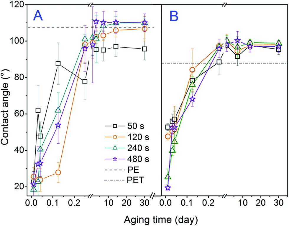 | ||
| Fig. 3 Dependence of the contact angle on the plasma exposure time (50–480 s) for different periods (from 15 min to 30 days) elapsed from the plasma treatment for: (A) PE and (B) PET. Dashed lines represent values of contact angle of pristine polymers. | ||
| Sample | Contact angle (°) | |
|---|---|---|
| PE | PET | |
| Polymer/120/Au | 100.6 ± 8.5 | 98.5 ± 2.1 |
| Polymer/120/Au/BPD | 102.0 ± 4.7 | 103.8 ± 5.3 |
| Polymer/120/Au/BPD/CuNP | 98.5 ± 2.5 | 100.0 ± 2.3 |
The chemical composition of the plasma treated PE and PET polymers with further modification by deposition of the gold layer, grafting with thiol groups and subsequently with CuNPs was studied using X-ray photoelectron spectroscopy (XPS). The survey spectra of PE and PET after each modification step are shown in Fig. 4A and B. The atomic concentrations of the elements C(1s) O(1s), Au(4f), S(2p) and Cu(2p3/2) are summarized in Table 2. From Table 2 it is evident that Ar plasma treatment leads to surface oxidation and the formation of polar functional groups (carbonyl, carboxyl, ester, etc.) on the surface of the polymers.29 The attachment of the biphenyldithiol layers to the surface of PE and PET was evidenced by the detection of sulphur with concentrations of 9.1 and 8.8 at%, respectively. The presence of copper atoms and a mild decrease in sulphur concentration have proved that the CuNP were successfully bonded via the BPD nanospacer. In the case of PET (1.6 at%) a higher amount of CuNP was grafted in comparison to PE (0.5 at%). For illustration, the deconvolution of Cu(2p3/2) peaks of (A) PE and (B) PET activated in plasma, coated with gold and then grafted with CuNPs through BPD linkers is shown in Fig. 5. In the case of PE (Fig. 5A) we can attribute particular components comprising the line of Cu 2p3/2 to the states Cu0 and Cu+. In the case of PET (Fig. 5B) it is possible to assign the component with binding energy 932.6 eV to the states Cu0 and Cu+; however the position with a binding energy at 934.8 eV cannot be assigned to the Cu2+ in oxide. Two possible explanations can be basically suggested. The charging of Cu atoms as a possible explanation could be attributed to the appearance of a dielectric “shell” encapsulating the particle. Since the shift in the satellite line of about 2.3 eV was not detected for other elements on the same sample, this explanation seems improbable. The other explanation, which also corresponds to some detected compounds ([N(C4H9)4]2[Cu(–CC(O)CC(S)C(S)–)2]; [N(C4H9)4]2[Cu(–C(S)C(S)C(O)C(O)–)2]) introduced in the database (http//www.srdata.gov), is that chemical bonds were created between Cu atoms and molecules from the deposition substrates (solutions). The binding energies cited in the database at the position of 934.8 eV correspond to this explanation. The observed discrepancies between the concentrations of CuNPs are due to specific changes in physico–chemical parameters after plasma treated covering: (i) surface chemical composition (number of functional places suitable for BPD grafting), (ii) sample roughness and (iii) the character of the anchored particle itself or (iv) the surface tension of the prepared samples.30
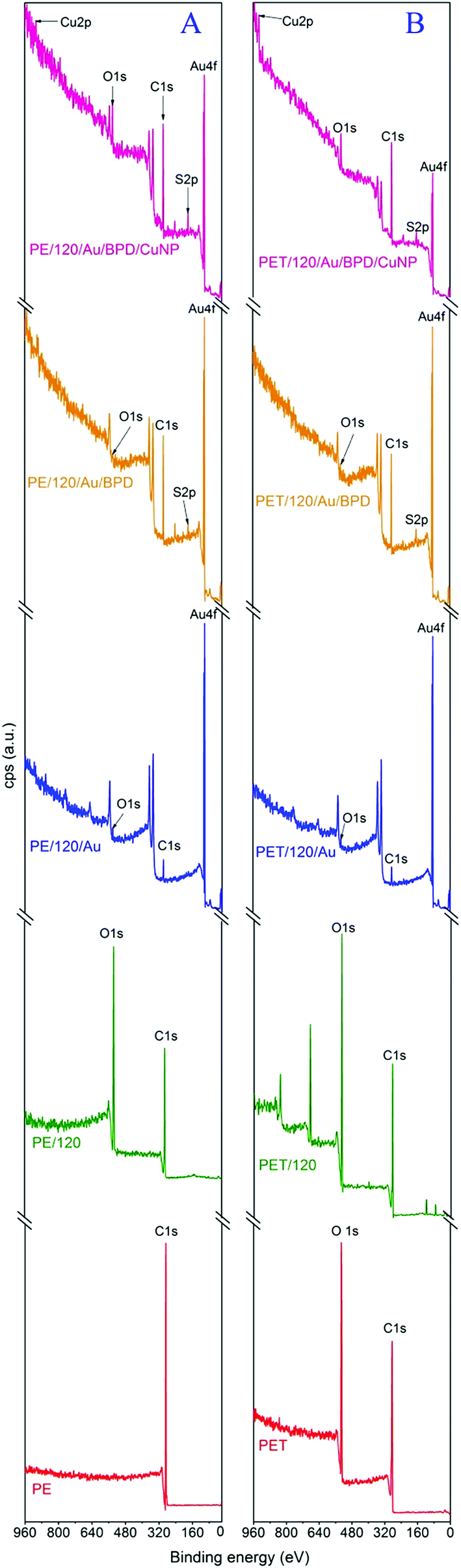 | ||
| Fig. 4 Survey XPS spectra of (A) PE and (B) PET: pristine (polymer); treated by plasma (polymer/120); plasma treated, gold coated polymer substrates (polymer/120/Au); plasma treated, gold coated and consequently grafted with BPD linkers (polymer/120/Au/BPD); activated in plasma, coated with gold and then grafted with CuNPs through BPD linkers (polymer/120/Au/BPD/CuNP). | ||
| Sample | Element concentration (at%) | ||||
|---|---|---|---|---|---|
| C(1s) | O(1s) | Au(4f) | S(2p) | Cu(2p3/2) | |
| PE | 100 | — | — | — | — |
| PE/120 | 77.8 | 22.2 | — | — | — |
| PE/120/Au | 44.4 | 7.9 | 47.7 | — | — |
| PE/120/Au/BPD | 69.1 | 2.7 | 19.1 | 9.1 | — |
| PE/120/Au/BPD/CuNP | 71.6 | 9.9 | 10.5 | 7.5 | 0.5 |
| PET | 73.7 | 26.3 | — | — | — |
| PET/120 | 67.0 | 33.0 | — | — | — |
| PET/120/Au | 41.6 | 6.2 | 52.2 | — | — |
| PET/120/Au/BPD | 68.1 | 3.6 | 19.5 | 8.8 | — |
| PET/120/Au/BPD/CuNP | 71.4 | 10.1 | 9.4 | 7.5 | 1.6 |
 | ||
| Fig. 5 Deconvolution of Cu(2p3/2) peak of (A) PE and (B) PET activated in plasma, coated with gold and then grafted with CuNPs through BPD linkers. Measured spectrum (black line) is compared with that fitted (orange line). The position and size of particular components are also shown. | ||
Energy-dispersive X-ray spectroscopy (EDS) was used to determine the elemental composition of the samples (see Table 3) and to map the elements (C, O, Au, S and Cu) on the sample's surface (see Fig. 6). The presence of sulphur and copper confirmed successful grafting of biphenyl-4,4′-dithiol and CuNPs. The sulphur concentration decreased after the nanoparticle grafting, due to their bonds with the thiol group. In the case of PET, a significantly higher concentration of oxygen was detected, because the oxygen is also present in the structure of the pristine polymer. Moreover, EDS revealed that CuNPs are homogeneously distributed over the whole surface. Surprisingly, it can be seen that sulphur tends to aggregate slightly and does not cover the substrate in the same manner as the MNPs. Similar to the XPS analysis we can see that the concentration of nanoparticles is higher on the PET substrate (0.4 wt%).
| Sample | Element concentration (wt%) | ||||
|---|---|---|---|---|---|
| C | O | Au | S | Cu | |
| PE/120/Au/BPD | 27.7 ± 0.3 | 1.0 ± 0.1 | 70.9 ± 0.3 | 0.4 ± 0.1 | — |
| PE/120/Au/BPD/CuNP | 33.0 ± 0.3 | 0.9 ± 0.1 | 65.6 ± 0.3 | 0.2 ± 0.1 | 0.3 ± 0.1 |
| PET/120/Au/BPD | 29.1 ± 0.6 | 4.6 ± 0.3 | 65.6 ± 0.7 | 0.7 ± 0.3 | — |
| PET/120/Au/BPD/CuNP | 26.4 ± 0.3 | 4.2 ± 0.1 | 68.6 ± 0.4 | 0.4 ± 0.1 | 0.4 ± 0.1 |
 | ||
| Fig. 6 EDS element distribution maps of plasma treated PE and PET (120 s), gold coated and grafted with biphenyl-4,4′-dithiol and then with CuNP (PE/120/Au/BPD/CuNP) or (PET/120/Au/BPD/CuNP): from left to right elements: C (red), O (cyan), Au (green), S (yellow), Cu (magenta). | ||
Results from the zeta potential determination are presented in Fig. 7. We observed earlier that plasma treatment alters the surface chemistry, charge and morphology.25 From Fig. 7 it is clear that after plasma treatment the surface chemistry changes significantly and the zeta potential increases due to the presence of newly developed oxygen groups on the surface (see also the data in Table 2). Differences in zeta potential values before and after plasma treatment are more pronounced on PE because oxygen is not present in the chemical structure of pristine PE in contrast to pristine PET. Au coating of polymer substrates leads to a shift in zeta potential to much more negative values in comparison with plasma treated samples, due to the presence of a metal nanolayer on both of the polymers.31 After BPD grafting the zeta potential decreases again due to two indistinguishable phenomena; (i) the presence of the carbon rings of BPD, which leads to a more hydrophobic surface and (ii) the presence of thiol groups on the surface, which deprotonate in aqueous solution, thus causing the surface charge to become more negative.25 More visible changes in surface chemistry and charge were obtained for PET in comparison with PE, which corresponds well with the EDS and XPS analyses.
 | ||
| Fig. 7 Zeta potential determined on PE and PET: pristine, plasma treated (time 120 s), plasma treated and gold coated; gold coated and grafted with dithiol (BPD) and then grafted with CuNPs (polymer/120/Au/BPD/CuNP). | ||
According to our previous research, we have confirmed that plasma treatment leads to alterations in the polymer surface morphology, and the significance of the changes depends on the type of polymer substrate. Thanks to ablation during the plasma treatment, it can be supposed that the PE amorphous phase is ablated faster than the crystalline phase, resulting in the creation of lamellar structures reflecting the arrangement of molecular chains on the PE surface. On the other hand, plasma treatment of PET causes only tiny, sharp formations which may represent low molecular oxidized structures (LMWOS) (data not shown, see ref. 32). AFM images of sample surface evaluation after each step of the preparation procedure are shown in Fig. 8. The gold was sputtered to form a uniform, electrically continuous layer with a globular nanostructure, as can be seen for both PE and PET (Fig. 8A); for the detail of the gold clusters, please see Fig. 9 (100 × 100 nm2). From Fig. 8 it can be clearly seen that we have prepared a nanostructured surface with clusters/nanowires, which is crucial for potentially exhibiting a large EF phenomenon. The grafting of samples with biphenyl-4,4′-dithiol causes significant changes on the polymer surface, which are more pronounced on PET. In the case of PET a significant increase in surface roughness induced by the formation of cluster structures was observed. The appearance of these structures, which are uniformly distributed over the whole surface is induced by biphenyl-4,4′-dithiol grafting on the Au layer and also the formation of higher structures up to 20 nm can be induced by etching of “soft-spots” in the Au/PET layer and consequent partial distortion of the surface. The globular structure is also changed when the grafting of BPD takes place (see Fig. 8B). The CuNPs are apparent on Fig. 8 (right) as the “second layer” of small globules and globular structures on PET/Au. Also the interaction with the Cu grafting solution caused the partial removal of BPD from the surface and thus the original globular nanostructure is more apparent on the surface. The changes on PE are less pronounced in comparison to grafted PET, which is in good agreement with EDS and XPS analyses. For comparison, we have introduced SEM images (Fig. 8D), which are in good agreement with the AFM images and confirm significant changes on the polymer surface after CuNP grafting.
 | ||
| Fig. 8 AFM images of PE and PET for: (A) plasma treated, gold coated polymer substrates (polymer/120/Au); (B) plasma treated, gold coated and consequently grafted with BPD linkers (polymer/120/Au/BPD); (C) activated in plasma, coated with gold and then grafted with CuNPs through BPD linkers (polymer/120/Au/BPD/CuNP). Ra is surface roughness in nm. (D) SEM images of PE and PET plasma treated, gold coated and grafted with CuNP via BPD linkers. | ||
 | ||
| Fig. 9 AFM images in greater detail (100 × 100 nm2) of plasma treated (120 s) and gold coated PE and PET, respectively. Ra is surface roughness in nm. | ||
The SERS spectra were determined on particular points on the sample surface (8 points). The average spectra of samples without and with CuNPs are introduced in Fig. 10. Predominantly “characteristic” rhodamine bands were detected on all samples without CuNPs.33,34 The positions of the stretching modes at 1650, 1573, 1510, 1363, 1311, 1187, 771 and 612 cm−1 were detected. New bands were detected in the spectra of the samples grafted with BPD. The bands at positions 1586, 1282 and 1081 cm−1 were present with similar intensity to the bands of R6G. Bands at ca. 1190 cm−1 were observed as a double-band where the maximum at 1192 cm−1 was assigned to BPD and the maximum at 1183 cm−1 was assigned to R6G. After CuNP grafting the vibrations of the aromatic rings were amplified.35 Furthermore, the stretching vibration of the C–C bond was amplified (the link between the rings in the molecule), at position 1286 cm−1. The band at 1193 cm−1, which is attributed to the bending HC![[double bond, length as m-dash]](https://www.rsc.org/images/entities/char_e001.gif) CH vibration was also enhanced; furthermore, no double-band indicating the presence of R6G signals as in the case of samples without CuNP was observed. As for the band at 1083 cm−1, which according the literature can be attributed to the C–S(Au) stretching vibration,36 it can be assumed that a chemical bond between the sulphur and copper atoms was created. An enhancement due to CuNPs grafting on the surface is apparent since high intensities of the BPD bands (at ca. 1589, 1283, 1191, 1082 cm−1 in the case of the PET substrate and at ca. 1589, 1284, 1193 and 1082 cm−1 in the case of the PE substrate) were observed. These bands were not detected with such intensity without employing CuNPs in either PE or PET substrates. Spectra of samples with CuNPs exhibited an intensity ratio between BPD and R6G which is much higher in comparison to spectra of samples without CuNPs, where the intensities of the BPD bands and R6G bands were similar. For an estimation of the enhancement factors, the band of the CC vibration mode in an aromatic ring at ca. 1589 cm−1 was used. The laser trace had a diameter of 5 μm, and the amounts of NPs and BPD molecules were evaluated from the XPS analysis. The final enhancement factors were 1.7 × 10³ and 0.9 × 10² for the PE and PET substrates, respectively.
CH vibration was also enhanced; furthermore, no double-band indicating the presence of R6G signals as in the case of samples without CuNP was observed. As for the band at 1083 cm−1, which according the literature can be attributed to the C–S(Au) stretching vibration,36 it can be assumed that a chemical bond between the sulphur and copper atoms was created. An enhancement due to CuNPs grafting on the surface is apparent since high intensities of the BPD bands (at ca. 1589, 1283, 1191, 1082 cm−1 in the case of the PET substrate and at ca. 1589, 1284, 1193 and 1082 cm−1 in the case of the PE substrate) were observed. These bands were not detected with such intensity without employing CuNPs in either PE or PET substrates. Spectra of samples with CuNPs exhibited an intensity ratio between BPD and R6G which is much higher in comparison to spectra of samples without CuNPs, where the intensities of the BPD bands and R6G bands were similar. For an estimation of the enhancement factors, the band of the CC vibration mode in an aromatic ring at ca. 1589 cm−1 was used. The laser trace had a diameter of 5 μm, and the amounts of NPs and BPD molecules were evaluated from the XPS analysis. The final enhancement factors were 1.7 × 10³ and 0.9 × 10² for the PE and PET substrates, respectively.
 | ||
| Fig. 10 SERS spectra of PE and PET for: (A) activated in plasma, coated with gold and then grafted with CuNPs through BPD linkers (polymer/120/Au/BPD/CuNP); (B) plasma treated, gold coated and consequently grafted with BPD linkers (polymer/120/Au/BPD); (C) plasma treated, gold coated polymer substrates (polymer/120/Au). R6G molecules were additionally deposited. | ||
4. Conclusion
We have demonstrated the preparation of sensitive SERS substrates based on CuNPs (capable of LSP excitation) assembled on gold layer sandwich structures (able to support SPP). The proposed plasmonic platform includes chemically synthesized CuNPs grafted through BPD linkers on the polymer/gold surface. For SERS evaluation, R6G molecules were additionally deposited onto prepared substrates. Successful grafting of thiols and synthesized CuNPs on the plasma treated surface of PE and PET was confirmed by goniometry, electrokinetic analysis, and spectroscopic (XPS and EDS) and microscopic (SEM, AFM) methods. The presence of sulphur in the XPS spectra (supported by EDS analysis) indicated the creation of a BPD interlayer on the plasma treated and gold coated surface. After the anchoring of CuNPs a slight decrease in sulphur concentration occurred as a consequence of the CuNPs shadow effect. Observed discrepancies between concentrations of CuNPs were due to specific changes in physico–chemical parameters after plasma activation covering: (i) surface chemical composition, (ii) sample roughness and (iii) the character of anchored particle itself or (iv) the surface tension of prepared samples. The concentration of CuNPs was higher on the PET substrate compared to PE. Also electrokinetic analysis confirmed more visible changes in surface chemistry and charge obtained for PET in comparison to PE. Sputtered gold formed a uniform, electrically continuous layer with a globular nanostructure on both PE and PET surfaces. In the case of PET, subsequent grafting of biphenyl-4,4′-dithiol caused a significant increase in surface roughness induced by the formation of cluster structures. These structures were uniformly distributed over the whole PET surface. CuNPs appeared as a “second layer” of small globules and globular structures on PET/Au. The changes in surface morphology on PE were less pronounced in comparison to grafted PET, which is in good agreement with the EDS and XPS analyses. The SEM images were in good agreement with the AFM images and confirmed significant changes in the polymer surface after CuNP grafting. The application of CuNP was followed by the higher signal of BPD, which was adsorbed via a thiol group, that was demonstrated by observation of a new band at ca. 1082 cm−1. From the SERS spectra of the system it was obvious that the enhancement in the signal for samples with CuNPs was significantly higher than on those without. The successful binding of CuNPs on Au film with a non-enhancing surface revealed a promising way to enhance the SERS signal on a gold nanolayer on a polymer. The enhancement factor was higher for PE (1.7 × 10³) compared to PET (0.9 × 10²). The studied systems could be helpful not only for theoretical research into the LSP-SPP effect by SERS but the metal-to-metal junctions could also have great applications in molecular electronic devices and biology.Acknowledgements
This work was supported by the Czech Science Foundation (GA CR) under the projects 17-00939S (AR) and 108/12/G108 (VS, PS). The authors acknowledge the assistance provided by the Research Infrastructure NanoEnviCz, supported by the Ministry of Education, Youth and Sports of the CR under Project No. LM2015073 (ZK).References
- M. Xia, P. Zhang, K. Qiao, Y. Bai and Y. H. Xie, J. Phys. Chem. C, 2016, 120, 527 CAS.
- W. E. Doering and S. M. Nie, J. Phys. Chem. B, 2002, 106, 311 CrossRef CAS.
- Y. L. Wang, X. Q. Zou, W. Ren, W. D. Wang and E. K. Wang, J. Phys. Chem. C, 2007, 111, 3259 CAS.
- E. Hutter, J. H. Fendler and D. Roy, J. Phys. Chem. B, 2001, 105, 11159 CrossRef CAS.
- C. J. Orendorff, A. Gole, T. K. Sau and C. J. Murphy, Anal. Chem., 2005, 77, 3261 CrossRef CAS PubMed.
- K. Kim and J. K. Yoon, J. Phys. Chem. B, 2005, 109, 20731 CrossRef CAS PubMed.
- J. K. Daniels and G. Chumanov, J. Phys. Chem. B, 2005, 109, 17936 CrossRef CAS PubMed.
- S. M. Nie and S. R. Emery, Science, 1997, 275, 1102 CrossRef CAS PubMed.
- R. F. Aroca, R. E. Clavijo, M. D. Halls and H. B. Schlegel, J. Phys. Chem. A, 2000, 104, 9500 CrossRef CAS.
- Y. Kalachyova, D. Mares, O. Lyutakov, M. Kostejn, L. Lapcak and V. Švorčík, J. Phys. Chem. C, 2015, 119, 9506 CAS.
- M. Litorja, C. L. Haynes, A. J. Haes, T. R. Jensen and R. P. Van Duyne, J. Phys. Chem. B, 2001, 105, 6907 CrossRef CAS.
- A. D. McFarland, M. A. Young, J. A. Dieringer and R. P. Van Duyne, J. Phys. Chem. B, 2005, 109, 11279 CrossRef CAS PubMed.
- M. Geissler, K. B. Li, B. Cui, L. Clime and T. Veres, J. Phys. Chem. C, 2009, 113, 17296 CAS.
- S. G. Jang, D. G. Choi, C. J. Heo, S. Y. Lee and S. M. Yang, Adv. Mater., 2008, 20, 4862 CrossRef CAS.
- N. C. Linn, C. H. Sun, A. Arya, P. Jiang and B. Jiang, Nanotechnology, 2009, 20, 225303 CrossRef PubMed.
- P. Zvatora, P. Rezanka, V. Prokopec, J. Siegel, V. Svorcik and V. Kral, Nanoscale Res. Lett., 2011, 6, 366 CrossRef PubMed.
- K. Kim and H. S. Lee, J. Phys. Chem. B, 2005, 109, 18929 CrossRef CAS PubMed.
- Y. Kalachyova, D. Mares, V. Jerabek, K. Zaruba, P. Ulbrich, L. Lapcak, V. Svorcik and O. Lyutakov, J. Phys. Chem. C, 2016, 120, 10569 CAS.
- J. Srajer, A. Schwaighofer, G. Ramer, S. Rotter, B. Guenay, A. W. Kriegner, W. Knoll, B. Lendl and C. Nowak, Nanoscale, 2014, 6, 127 RSC.
- M. D. Porter, R. J. Lipert, L. M. Siperko, G. Wang and R. Narayanan, Chem. Soc. Rev., 2008, 37, 1001 RSC.
- A. Reznickova, M. Orendac, Z. Kolska, E. Cizmar, M. Dendisova and V. Svorcik, Appl. Surf. Sci., 2016, 390, 728 CrossRef CAS.
- M. Dendisova-Vyskovska, V. Prokopec, M. Clupek and P. Matejka, J. Raman Spectrosc., 2012, 43, 181 CrossRef CAS.
- V. Švorčík, A. Chaloupka, K. Záruba, V. Král, O. Bláhová and A. Macková, Nucl. Instrum. Methods Phys. Res., Sect. B, 2009, 267, 2484 CrossRef.
- V. Švorčík, Z. Kolská, O. Kvítek, J. Siegel, A. Řezníčková, P. Rezanka and K. Zaruba, Nanoscale Res. Lett., 2011, 6, 607 CrossRef PubMed.
- Z. Kolská, A. Řezníčková, M. Nagyová, N. Slepičková Kasálková, P. Sajdl, P. Slepička and V. Švorčík, Polym. Degrad. Stab., 2014, 101, 1 CrossRef.
- M. Homberger and U. Simon, Philos. Trans. R. Soc., A, 2010, 368, 1405 CrossRef CAS PubMed.
- J. M. Grace and L. J. Gerenser, Prog. Polym. Sci., 2003, 24, 305 CAS.
- C. M. Chan, T. M. Ko and H. Hiraoka, Surf. Sci. Rep., 1996, 24, 1 CrossRef CAS.
- P. K. Chu, J. Y. Chen, L. P. Wang and N. Huang, Mater. Sci. Eng., R, 2002, 36, 143 CrossRef.
- S. Gam-Derouich, S. Mahouche-Chergui, S. Truong, D. B. Hassen-Chehimi and M. M. Chehimi, Polymer, 2011, 52, 4463 CrossRef CAS.
- Z. Kolská, A. Řezníčková, O. Kvítek and V. Švorčík, J. Nanosci. Nanotechnol., 2012, 12, 6652 CrossRef.
- A. Řezníčková, Z. Kolská, V. Hnatowicz, P. Stopka and V. Švorčík, Nucl. Instrum. Methods Phys. Res., Sect. B, 2011, 269, 83 CrossRef.
- A. M. Michaels, M. Nirmal and L. E. Brus, J. Am. Chem. Soc., 1999, 121, 9932 CrossRef CAS.
- A. M. Michaels, J. Jiang and L. Brus, J. Phys. Chem. B, 2000, 104, 11965 CrossRef CAS.
- P. Z. El-Khoury, D. H. Hu, V. A. Apkarian and W. P. Hess, Nano Lett., 2013, 13, 1858 CrossRef CAS PubMed.
- I. Georgieva and N. Trendafilova, J. Phys. Chem. A, 2007, 111, 13075 CrossRef CAS PubMed.
| This journal is © The Royal Society of Chemistry 2017 |