 Open Access Article
Creative Commons Attribution 3.0 Unported Licence
Dynamic conductance characteristics in HfOx-based resistive random access memory
Ying-Chen Chen*a,
Yao-Feng Chang a,
Xiaohan Wua,
Fei Zhoua,
Meiqi Guoa,
Chih-Yang Linb,
Cheng-Chih Hsieha,
Burt Fowlera,
Ting-Chang Changb and
Jack C. Leea
aMicroelectronics Research Center, Department of Electrical and Computer Engineering, The University of Texas at Austin, Austin, Texas 78758, USA. E-mail: yingchenchen@utexas.edu
bDepartment of Physics, National Sun Yat-Sen University, Kaohsiung 804, Taiwan
First published on 24th February 2017
Abstract
Characteristics of HfOx-based resistive switching memory (RRAM) in Al/HfOx/Al and Al/AlOx/HfOx/Al structures were studied using a dynamic conductance method. Step-like RESET behaviors as well as pre- and post-RESET regions of operation were characterized. The results indicated that defects at the oxide interface caused cycling issues in the Al/AlOx/HfOx/Al structure. No such RESET behavior was observed for the Al/HfOx/Al structure. Current induced over-heating, which caused an early RESET event, could be avoided using current-sweep technique that caused less electrical and thermal stress in localized regions. The experimental results not only provided insights into potential reliability issues and power management in HfOx-based RRAM, but also helped clarifying the resistive switching mechanisms.
Introduction
Resistive random access memory (RRAM) has attracted a great attention as a potential candidate for next-generation emerging memory devices due to its high switching speed, excellent scalability, low-voltage operation and multilevel storage.1–4 There have been numerous studies on binary metal oxides such as FeOx, ZrOx, TiO2, NiO, Al2O3, CuxO, and HfOx.5–11 These metal–insulator–metal structures exhibit resistance switching characteristics due to the inevitable existence of non-stoichiometry in the insulating thin film. Among these insulators, hafnium oxide (HfOx) was proposed as the most promising material system based on the 2015 International Technology Roadmap for Semiconductors (ITRS) due to its overall performances on the reliability, including endurance property (>1012 cycles), retention (>10 years at 85 °C), and operation stability (i.e. current limiting operation) conformed with the requirements of non-volatile memory and storage class memory applications.12 Furthermore, HfOx as a dielectric layer was extensively studied and used as the gate dielectrics for MOSFETs since 45 nm technology node and is obviously compatible with the complementary metal–oxide–semiconductor (CMOS) process. In this study, a dynamic conductance method, i.e. derivative of DC I–V response (∂I/∂V), was used to study the HfOx-based RRAM characteristics in Al/HfOx/Al and Al/AlOx/HfOx/Al structures. HfOx-based devices have been reported to exhibit good switching properties in different operating polarities in four quadrants.13 This dynamic conductance method can be used to study the RESET behaviors in bipolar switching as well as in unipolar switching. Analyzing the dynamic conductance can help understand the RESET behaviors (e.g. one-step-like and multi-step-like) and filament degradation characteristics in the pre- and post-RESET regions of operation, which provide defect density information at the oxide interface with the explanation of cycling issue in Al/AlOx/HfOx/Al structure. On the other hand, using current-sweep operation, an early RESET event can be avoided due to reduced current induced over-heating, which provides insights and optimization for power management in HfOx-based RRAM. The dynamic conductance technique and the experimental results not only help to identify resistive switching mechanisms, but also construct a model to predict the operating performance of HfOx-based RRAM device for future device designs and applications.Experimental
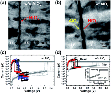
Al (100 nm)/HfOx (10 nm)/Al (210 nm) and Al (100 nm)/AlOx (5 nm)/HfOx (10 nm)/Al (210 nm) bilayer-insulator devices were fabricated (see transmission electron microscope (TEM) images in Fig. 1(a) and (b)). Starting substrates were heavily-doped N+ Si wafers. First, buffered-oxide-etch (BOE) was used to remove any native oxide layer on the substrate, followed by acetone and isopropyl alcohol (IPA) rinses. Aluminum (210 nm thick) was deposited on the N+ Si substrate as the bottom electrode using e-beam evaporation at a pressure of less than 10−5 Torr. There may exist a thin layer (∼2 nm) of unintended AlOx even though we deposited the HfOx subsequently after Al BE since Al is easily oxidized even at low temperature. This thin layer had a good influence and improvement on the uniformity and reliability of performance.14 Then, 10 nm-thick resistive switching (RS) dielectric layers of HfOx were deposited using atomic layer deposition (ALD) with precursor (TEMAH, i.e. tetrakis(ethylmethylamino)hafnium) and H2O in a ratio of 1![[thin space (1/6-em)]](https://www.rsc.org/images/entities/char_2009.gif) :
:![[thin space (1/6-em)]](https://www.rsc.org/images/entities/char_2009.gif) 3 at 250 °C. For Al (100 nm)/AlOx (5 nm)/HfOx (10 nm)/Al (210 nm) bilayer RRAM devices, the AlOx was deposited on the top of the HfOx layer using ALD with a precursor (TMA, i.e. trimethylaluminum) and H2O in a ratio of 2
3 at 250 °C. For Al (100 nm)/AlOx (5 nm)/HfOx (10 nm)/Al (210 nm) bilayer RRAM devices, the AlOx was deposited on the top of the HfOx layer using ALD with a precursor (TMA, i.e. trimethylaluminum) and H2O in a ratio of 2![[thin space (1/6-em)]](https://www.rsc.org/images/entities/char_2009.gif) :
:![[thin space (1/6-em)]](https://www.rsc.org/images/entities/char_2009.gif) 3 at 250 °C. HfOx was deposited using the same method described above. Then, Al (100 nm) was deposited using e-beam evaporation as the top electrode for both HfOx and AlOx/HfOx RRAM devices. The top electrodes of various sizes (diameters of 30, 60, 150 μm) were patterned using the lift-off method. Through energy dispersive spectrometer (EDS) results (data not shown), the material compositions and stoichiometry including Al top electrode, AlOx (x = 1.8) and HfOx (x = 2.3) of the Al/AlOx/HfOx/Al device structure were verified. Agilent B1500 and Lakeshore probe stations were used for electrical characterization of both HfOx-based RRAM structures.
3 at 250 °C. HfOx was deposited using the same method described above. Then, Al (100 nm) was deposited using e-beam evaporation as the top electrode for both HfOx and AlOx/HfOx RRAM devices. The top electrodes of various sizes (diameters of 30, 60, 150 μm) were patterned using the lift-off method. Through energy dispersive spectrometer (EDS) results (data not shown), the material compositions and stoichiometry including Al top electrode, AlOx (x = 1.8) and HfOx (x = 2.3) of the Al/AlOx/HfOx/Al device structure were verified. Agilent B1500 and Lakeshore probe stations were used for electrical characterization of both HfOx-based RRAM structures.
Results and discussion
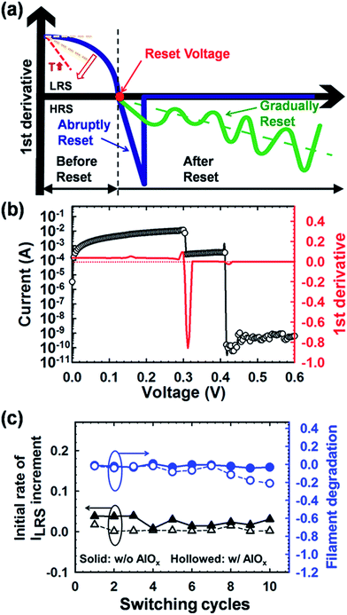
Fig. 1(c) and (d) show the RS I–V curves during DC voltage sweeps for HfOx-based RRAM devices with and without AlOx, respectively. We fabricated AlOx (5 nm)/HfOx of (3, 5 and 10 nm) stacking devices, and the performance of HfOx with varied thickness was studied. Both the switching voltage and memory window were independent of the HfOx thickness. Therefore, Al/HfOx (10 nm)/Al and Al/AlOx (5 nm)/HfOx (10 nm)/Al structures were used to demonstrate this dynamic conductance method. Voltage was applied to the top electrode (Al) with the bottom electrode (Al) at ground. All the testing was done in ambient air. Unipolar switching was observed for these two device structures (Fig. 1). First, a one-step electroforming (inset in Fig. 1(c)) process was used: (1) a compliance current-limited (CCL) voltage sweep to induce soft breakdown and (2) a forward voltage sweep to electroform the device. In other words, soft breakdown in the insulator occurred when voltage was swept until the current dramatically increased to a CCL voltage of 1 μA. Generally, this current compliance was used to prevent a hard breakdown (i.e. permanent breakdown) of oxide layers during the forming process. After the electroforming, the RS performance was stabilized by cycling multiple times using DC voltage sweeps. Then, a SET process was applied by a forward/reverse sweep with 1 mA CCL to program the device to the low resistance state (LRS). As shown in Fig. 1(c) and (d), the SET voltage for RRAMs with and without AlOx was approximately 2.2 V and 1.8 V, respectively. The RESET process was applied by sweeping the voltage to the value where the current decreased abruptly to program the devices to a high resistance state (HRS). The RESET voltage for RRAMs with and without AlOx was approximately 1 V and 0.8 V, respectively (see Fig. 1(c) and (d)). The LRS/HRS current ratio was ∼107 and 104 at 0.1 V read voltage for the RRAM devices with and without AlOx, respectively.To investigate RESET mechanisms, I–V curves were analyzed using the dynamic conductance method (i.e. ∂I/∂V) in two regions (i.e., pre-RESET and post-RESET). During the RESET sweep to ∼0.8–1 V, current began to drop at the RESET voltage (VRESET) and the device was programmed to HRS. With identical SET CCL of 1 mA, multi-step-like and one-step-like RESET were observed in RRAM with and without AlOx (Fig. 1(c) and (d)). In other words, by adding AlOx in the switching layers, the RESET I–V transition above VRESET changed from one-step fall-off to multiple fall-off in current resulting in different HRS states. This difference could be contributed to the high defect density at the interface between the AlOx and HfOx layers, leading to the abrupt current drop during filament rupturing in the RESET process.15,16 In contrast, the SET process showed no multiple SET behaviors in these two structures. Analyzing plots of I–V dynamic conductance (or 2nd derivative) can help understand the RESET mechanism and further clarify the fall-off process where the filament degrades/ruptures during the RESET process. Fig. 2(a) shows a schematic of the temperature dependence in the pre-RESET region, cycling capability, and device structure dependence observed in the 1st derivative/2nd derivative plots for devices with (green curve) and without AlOx (blue curve). These dynamic conductance characteristics (1st derivative/2nd derivative analyses) can help to verify that the fundamental filament degradation behaviors were enhanced in devices without AlOx compared to devices with AlOx for these variables under cycling analyses (more discussion in Fig. 2(c), shows that the unnecessary heat resulting in filament degradation in the pre-RESET region can be avoided). For the post-RESET region, temperature dependent dynamic conductance characteristics could further confirm the statement of unnecessary heat induced filament degradation in the pre-RESET region (called an early RESET event in LRS), and help to clarify the one-step fall-off RESET process and the multi-step fall-off current drop between these two structures (more discussion in Fig. 3, diffusion-driven and electrical-driven RESET behavior). Fig. 2(b) shows the I–V curve and the dynamic conductance plot of RRAM devices with AlOx, which provides the switching parameters, such as intercept of dynamic conductance (at 0 V), the tangential slope of the dynamic conductance at the intercept (at 0 V), and the slope of dynamic conductance (>zero bias region), which is described in further detail in Fig. 2(c) and 3.
 | ||
| Fig. 3 (a) Filament degradation as a function of temperature pre- and post-RESET, (b) non-zero counts in 2nd derivative. | ||
Fig. 2(c) shows the cycling effect on the initial rate of ILRS increment (i.e. the first derivative) and filament degradation for the two RRAM devices. The initial rate of ILRS increment is defined as the intercept of dynamic conductance curve, which is shown by the red curve in Fig. 2(b), and filament degradation is defined as the tangential slope of the dynamic conductance at the intercept. The initial rate of ILRS increment was higher for RRAM devices without AlOx, which indicated that the RRAM without AlOx reached the RESET current faster than RRAM with AlOx (see the black curve in Fig. 2(c)). The initial rate of ILRS increment values in Al/AlOx/HfOx/Al structure were quite close to zero for all 10 cycles, which indicated that the filament was weaker than the Al/HfOx/Al structure even in the zero-bias region due to the growth of filament being limited by the internal filament effect, which potentially triggered the RESET event earlier (in Al/HfOx/Al, the values were positive, which means that the LRS or filament continues increasing or growing).17 A similar scenario could be observed in the filament degradation analysis (blue curve in Fig. 2(c)); RRAM with AlOx having worse filament degradation after eight cycles (the larger of negative values (e.g. −0.2)). This implies that the filament was already in the self-compliance region (the tangential slope of the dynamic conductance has three cases: slope > 0, the filament continues growth; slope ∼ 0, filament self-limiting behavior; and slope < 0, RESET transition beginning) and would run into the RESET transition at the zero-bias region, which indicated that the generated current-induced Joule heating by DC cycling severely affected the filament degradation rate in the Al/AlOx/HfOx/Al structure. With a higher initial rate for the ILRS increment, the unnecessary heat resulting in filament degradation in the pre-RESET region could be avoided for RRAM without AlOx. In other words, the RRAM without AlOx is more desirable due to potentially less electrical or thermal stress than in the Al/AlOx/HfOx/Al structure and less cycle-induced filament degradation. In addition, this filament degradation of RESET behaviors has an important correlation with endurance failure.
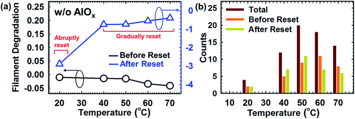
Fig. 3(a) shows the filament degradation as a function of operating temperature for the pre- and post-RESET regions on RRAM without AlOx. The filament degradation (i.e. the slope of dynamic conductance) in the pre-RESET region (>zero bias region, as shown in Fig. 2(a)) is caused by a sequence of random defect events, i.e. a defect injection into the filament or extraction from the filament. The value of 2nd derivative due to dynamic resistance change of filament (Fig. 2(c)) was then analyzed using a linear fitting method to obtain the overall slope, which was negative in the pre-RESET region, as shown in Fig. 2(a). The LRS filament degradation was caused by discrete defects migration, which correlates to a random value of activation energy (Ea) and a corresponding migration rate.18,19 With increasing operating temperature up to 60 °C, filament degradation begins to occur in the pre-RESET region. The filament degradation was much more severe in post-RESET (ruptured) than in the pre-RESET processes at room temperature (value of −3 vs. 0). For the pre-RESET region, the filament degradation deteriorated with increasing temperature after 50 °C (from −0.01 to −0.05). However, for the post-RESET region, the filament degradation became less negative with increasing temperature from 40 °C to 70 °C. This can be explained by diffusion-driven (i.e. highly temperature-dependent) RESET behavior in post-RESET process, which means gradual-RESET behavior occurs other than an abrupt RESET.20–22 On the other hand, the electrical-driven RESET behavior can explain the post-RESET region, i.e. the abrupt RESET with larger filament degradation (value of −3) at 20 °C in Fig. 3(a).
Fig. 3(b) shows the non-zero fluctuation counts in the 2nd derivative of the RESET I–V curve from 20 to 70 °C. The non-zero fluctuation counts indicate the observation of smooth curve-like continuous gradual RESET switching behavior instead of an abrupt RESET one. The more non-zero fluctuation indicated highly gradual RESET-like behavior. In the pre-RESET region, the counts increased with increasing temperature due to thermal disturbance, leading to filament degradation and increasing probability of early RESET on LRS. In other words, the increasing fluctuation may result from the increasing probability to either inject into or extract out of the conductive filament even under a thicker filament condition, i.e. LRS. In the post-RESET region, the counts increased with increasing temperature up to 50 °C and showed the temperature-induced gradual RESET. This is due to the fact that the rate of defect injection exceeded the rate of extraction among the discrete defect migration during the RESET transition. This phenomenon retarded after 50 °C, possibly due to current induced over-heating (or self-accelerated by Joule heating) in a localized region,23 which in turn caused abrupt RESET and highly efficient rupture of the filament. Thus, by suppressing the accelerated self-heating process in unipolar-type resistive switching, a precise control of filament temperature and localized switching phenomena could be achieved. This provides a possible solution for an early RESET event on LRS.24,25
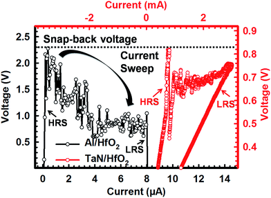
Fig. 4 and 5 show the data obtained by the current-sweep technique during the SET process. The current sweep technique is known to prevent device hard-breakdown and current overshoot failures (i.e. less electrical and thermal stress).26 The typical current-sweep I–V curves of Al/HfOx/Al and TaN/HfOx/Al devices are shown in Fig. 4. In contrast to the I–V curves using voltage-sweep, there were multiple states observed between the LRS and HRS in both Al/HfOx/Al and TaN/HfOx/Al RRAM devices. These multiple intermediate states can potentially be used for multi-level memory application by controlling the CCL in the SET process and RESET stop voltage in the RESET process, respectively. Moreover, the snap-back voltage, i.e. the maximum sensing voltage, could be observed during the current-sweep process where the resistance state begins to change from HRS to LRS. Through the SET process, the voltage across the device continued to increase as the current was swept up until a certain current endpoint was reached, i.e. LRS, where the “snap back voltage” is. The multiple voltage snap-back observation reflected the gradual RESET process of the conductive filament, suggesting that the broken conductive filament built up again gradually in the HfOx layer.27 The SET voltage was relatively higher in Al/HfOx/Al than in TaN/HfOx/Al devices potentially due the competitive oxygen vacancies affinity between the Al electrode and TaN electrode, e.g. the enthalpy of formation for of TaN and Al, −252.3 kJ mol−1 and 577.5 kJ mol−1, respectively.28,29
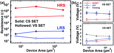 | ||
| Fig. 5 Device area effect of Al/HfOx/Al RRAM (a) on the HRS and LRS, (b) on forming and switching voltage by voltage-sweep (VS) and current-sweep (CS) methods. | ||
The effect of device area by current-sweep in the Al/HfOx/Al device compared to the voltage-sweep measurement technique is shown in Fig. 5(a) and (b). It was found that LRS and HRS currents (Fig. 5(a)), as well as the SET and RESET voltages (Fig. 5(b)) were independent of device area, illustrating that charge transport and RS occurred in a localized region along a conductive filament.30 Consistently, it provided further switching voltage reduction using current-sweep (Fig. 5(b), 0.6–1.4 V for the current-sweep and 1.5–2.8 V for the voltage-sweep). This voltage reduction may be a result of heat-induced defect injection that could improve the programming efficiency than an electrical-field driven process in a localized region along a conductive filament. The structure of filament changes was due to defect injection/extraction during programing.31 The current sweep technique not only improves data acquisition and enhances the understanding of the physics related to the SET process, but also provides the power management capability in a localized region for further reduction of current induced over-heating in an early RESET event on LRS.
Conclusions
In conclusion, early partial RESET phenomenon was investigated using dynamic conductance analysis, and the SET voltage was found to be reduced using a current-sweep programing method compared to a voltage-sweep method. High on/off current ratios of ∼104 with suitable switching voltage (<2 V) for Al/HfOx/Al RRAM were obtained. Through dynamic conductance analysis, one-step-like and multi-step-like RESET behaviors in the pre-RESET and post-RESET regions were investigated. Partial RESET within the pre-RESET region was observed in Al/AlOx/HfOx/Al RRAM by the cycling test, owing to high defect density at the AlOx/HfOx interface. The filament degradation phenomenon in the pre-RESET region deteriorated with increasing temperature. Using the current-sweep technique, the SET voltage was reduced to half of that obtained by voltage-sweep operation, which provided advantages of less electrical and thermal stress for power management capability in a localized region for future low power applications.Authors contribution
J. C. Lee and T. C. Chang designed research, Y. C. Chen and F. Zhou designed the experimental setup and performed the experiments, Y. C. Chen, M. Guo, C. Y. Lin, C. C. Hsieh, and X. Wu analyzed the data, and Y. C. Chen, B. Fowler and Y. F. Chang and J. C. Lee interpreted the results and wrote the paper. All authors read and approved the final version.References
- U. Chand, K. C. Huang, C. Y. Huang and T. Y. Tseng, IEEE Trans. Electron Devices, 2015, 62, 3665 CrossRef CAS
.
- R. Waser and M. Aono, Nat. Mater., 2007, 6, 833 CrossRef CAS PubMed
.
- Y. F. Chang, B. Fowler, Y. C. Chen, F. Zhou, C. H. Pan, T. C. Chang and J. C. Lee, Sci. Rep., 2016, 6, 21268 CrossRef CAS PubMed
.
- H. S. P. Wong, H.-Y. Lee, S. Yu, Y. S. Chen, Y. Wu, P. S. Chen, B. Lee, F. T. Chen and M. J. Tsai, Proc. IEEE, 2012, 100, 1951 CrossRef CAS
.
- S. B. Lee, S. C. Chae, S. H. Chang and C. Liu, Korean Appl. Phys., 2007, 51, 96 Search PubMed
.
- D. S. Lee, H. J. Choi, H. J. Sim, D. H. Choi, H. S. Hwang, M. J. Lee, S. A. Seo and I. K. Yoo, IEEE Electron Device Lett., 2005, 26, 900 CrossRef
.
- K. M. Kim, B. J. Choi, D. S. Jeong and C. S. Hwang, Appl. Phys. Lett., 2006, 89, 162912 CrossRef
.
- S. Seo, M. J. Lee, D. H. Seo, E. J. Jeoung, D. S. Suh, Y. S. Joung, I. K. Yoo, I. R. Hwang, S. H. Kim, I. S. Byun, J.-S. Kim, J. S. Choi and B. H. Park, Appl. Phys. Lett., 2004, 85, 5655 CrossRef CAS
.
- C.-Y. Lin, C.-Y. Wu, C.-Y. Wu, C. Hu and T.-Y. Tseng, J. Electrochem. Soc., 2007, 154, 189 CrossRef
.
- R. Dong, D. S. Lee, W. F. Xiang, S. J. Oh, D. J. Seong, S. H. Heo, H. J. Choi, M. J. Kwon, S. N. Seo, M. B. Pyun, M. Hasan and H. Hwang, Appl. Phys. Lett., 2007, 90, 042107 CrossRef
.
- L. W. Feng, C. Y. Chang, Y. F. Chang, W. R. Chen, S. Y. Wang, P. W. Chiang and T. C. Chang, Appl. Phys. Lett., 2010, 96(5), 052111 CrossRef
.
- K. C. Chang, T. C. Chang, T. M. Tsai, R. Zhang, Y. C. Hung, Y. E. Syu, Y. F. Chang, M. C. Chen, T. J. Chu, H. L. Chen, C. H. Pan, C. C. Shih, J. C. Zheng and S. M. Sze, Nanoscale Res. Lett., 2015, 10, 120 CrossRef PubMed
.
- B. Traoré, P. Blaise, E. Vianello, L. Perniola, B. De Salvo and Y. Nishi, IEEE Trans. Electron Devices, 2016, 63, 360–368 CrossRef
.
- D. S. Jeong, K. M. Kim, S. Kim, B. J. Choi and C. S. Hwang, Adv. Electron. Mater., 2016, 2, 1600090 CrossRef
.
- F. Yuan, S. Shen, Z. Zhang, L. Pan and J. Xu, Superlattices Microstruct., 2016, 91, 90–97 CrossRef CAS
.
- F. Yuan, Z. Zhang, L. Pan and J. Xu, IEEE J. Electron Devices Soc., 2014, 2(6), 154–157 CrossRef
.
- Y. F. Chang, B. Fowler, F. Zhou, Y. C. Chen and J. C. Lee, Appl. Phys. Lett., 2016, 108(3), 033504 CrossRef
.
- F. Yuan, S. Shen, Z. Zhang, L. Pan and J. Xu, Superlattices Microstruct., 2016, 91, 90–97 CrossRef CAS
.
- S. Ambrogio, S. Balatti, A. Cubeta, A. Calderoni, N. Ramaswamy and D. Ielmini, IEEE Trans. Electron Devices, 2014, 61(8), 2912–2919 CrossRef CAS
.
- F. Zhou, Y. F. Chang, Y. C. Chen, X. Wu, Y. Zhang, B. Fowler and J. C. Lee, Phys. Chem. Chem. Phys., 2016, 18(2), 700–703 RSC
.
- Y. F. Chang, Y. T. Tsai, G. W. Chang, Y. E. Syu, Y. H. Tai and T. C. Chang, ECS J. Solid State Sci. Technol., 2012, 1(5), Q91–Q95 CrossRef CAS
.
- P. Sun, L. Li, N. Lu, Y. Li, M. Wang, H. Xie and M. Liu, J. Comput. Electron., 2014, 13, 432 CrossRef
.
- U. Russo, C. Cagli, S. Spiga, E. Cianci and D. Ielmini, IEEE Electron Device Lett., 2009, 30, 817 CrossRef CAS
.
- U. Russo, D. Ielmini, C. Cagli and A. L. Lacaita, IEEE Trans. Electron Devices, 2009, 56, 193 CrossRef CAS
.
- I. H. Inoue, S. Yasuda, H. Akinaga and H. Takagi, Phys. Rev. B: Condens. Matter Mater. Phys., 2008, 77, 035105 CrossRef
.
- F. Zhou, Y. F. Chang, B. Fowler, K. Byun and J. C. Lee, Appl. Phys. Lett., 2015, 106(6), 063508 CrossRef
.
- M. H. Li, presented in part at 14th Annual Non-Volatile Memory Technology Symposium (NVMTS), Korea, October, 2014 Search PubMed
.
- J. A. Dean, Lange's handbook of chemistry, New York McGraw-Hill, 12th edn, 1979 Search PubMed
.
- E. Bauer, Appl. Surf. Sci., 1982, 11, 479–494 CrossRef
.
- Y. F. Chang, B. Fowler, Y. C. Chen, Y. T. Chen, Y. Wang, F. Xue, F. Zhou and J. C. Lee, J. Appl. Phys., 2014, 116(4), 043708 CrossRef
.
- Y. F. Chang, B. Fowler, Y. C. Chen and J. C. Lee, Prog. Solid State Chem., 2016, 44(3), 75–85 CrossRef CAS
.
| This journal is © The Royal Society of Chemistry 2017 |

