
 Open Access Article
 This Open Access Article is licensed under a Creative Commons Attribution-Non Commercial 3.0 Unported Licence
High-quality cadmium stannate annealed in N2 atmosphere for low-cost thin film solar cell†
Zhongming Du ab,
Xiangxin Liu*ab,
Yufen Zhangab and
Ziyao Zhua
ab,
Xiangxin Liu*ab,
Yufen Zhangab and
Ziyao Zhua
aThe Key Laboratory of Solar Thermal and Photovoltaic System, Institute of Electrical Engineering, Chinese Academy of Sciences, Beijing 100190, China. E-mail: shine@mail.iee.ac.cn; Fax: +86 10 8254 7041; Tel: +86 10 8254 7044
bUniversity of Chinese Academy of Sciences, Beijing 100049, China
First published on 28th March 2017
Abstract
Radio frequency magnetron sputtered cadmium stannate (Cd2SnO4) or cadmium tin oxide (CTO) films were annealed in a nitrogen (N2) atmosphere. The resistivity of argon/oxygen (Ar/O2) gas sputtered CTO films decreased drastically after high temperature annealing, and the lowest resistivity of 1.73 × 10⁻⁴ Ω cm was achieved. The Cd2SnO4 crystal phase of CTO films deposited in Ar/O2 gas occurred after annealing at 600 °C to 635 °C, and the optical band gap increased obviously after annealing. When the deposition atmosphere was pure Ar, the as-deposited CTO resistivity was in the order of 10−4 Ω cm. The resistivity of thin films deposited in Ar gas could decline slightly after annealing. However, the resistivity of thick films deposited under Ar gas increased drastically after annealing. No Cd2SnO4 crystal phase of Ar gas sputtered CTO occurred after annealing. The visible region and near infrared spectrum transmittance of CTO films increased after annealing in a N2 atmosphere. The resistivity of CTO films deposited in Ar/O2 and after annealing in N2 gas at 620 °C increased slightly after chlorine treatment. Furthermore, the resistivity of films deposited in Ar/O2 and then annealed in N2 gas at 620 °C decreased slightly after vacuum annealing at 600 °C for 5 min.
1. Introduction
Cadmium stannate (Cd2SnO4) is an important type of transparent conducting oxide and is widely used because it is similar to indium tin oxide. In 2004, cadmium tin oxide (CTO) received much attention because of the high efficiency of 16.7% that was generated using a cadmium tellurium (CdTe) adapted CTO as a transparent electrode.1 Many methods are available to produce CTO films. Among these methods, magnetron sputtering is an effective technique. Some studies on CTO were carried out after CTO film was first deposited in 1972.2 Furthermore, the treatment of sputtered CTO films at high temperature is continuously studied. One of the important features of annealing research, is the annealing atmosphere. Properties of CTO films after annealing in an argon (Ar) atmosphere,3,4 argon/cadmium sulfide (Ar/CdS) atmosphere,5–8 helium (He) and hydrogen (H2) atmosphere,9 dry air atmosphere,10 He/CdS atmosphere11 and Cd atmosphere12 have been studied. As far as is known, there has been no research on annealing sputtered CTO in a nitrogen (N2) atmosphere. Meanwhile, almost all the CTO films with a resistivity below 2 × 10⁻⁴ Ω cm require the presence of CdS during annealing. This finding links the CTO film properties to the subsequent fabrication process of a CdS/CdTe solar cell and means that the cell performance optimisation delicate. In the research reported here, radio frequency (RF) magnetron sputtered CTO with a resistivity as low as 1.73 × 10⁻⁴ Ω cm was fabricated by annealing in a low cost and abundant N2 atmosphere without the presence of CdS. Optimisation of both the optical and electrical properties of CTO films was carried out by controlling the annealing process in N2.2. Experimental
CTO films were deposited by sputtering from a hot-pressed ceramic target with a diameter of 76 mm on a 10 cm × 10 cm Corning 7059 glass substrate. Before deposition, the substrate was cleaned in a Micro-90 solution with a mass concentration of 2% and then rinsed with deionised water. The deposition chamber was evacuated to a base pressure of as low as 5 × 10⁻⁴ Pa. Sputtering was then performed in pure Ar or an Ar/oxygen (O2) mixture at a pressure of 1.5 Pa. When the Ar/O2 mixed gas was used for sputtering, the Ar![[thin space (1/6-em)]](https://www.rsc.org/images/entities/char_2009.gif) :O2 ratio was maintained at a ratio of 8:2. The RF power density was fixed at 1.775 W cm−2. The target to substrate distance was kept at 7 cm. The substrate was not intentionally heated during the deposition. Films with different thicknesses were deposited in both pure Ar and Ar/O2. After the deposition, the substrates were cut into quarter pieces and annealed in N2 at a flow rate of 1500 mL min−1 after 10 min purging with pure N2. Annealing was performed between 560 °C and 635 °C for 30 min. Even though CTO film is resilient up to 900 °C,13 the annealing temperature is limited by the softening point of the 7059 glass at 639 °C.14 Therefore, the annealing temperature in this work was always set below 635 °C. Cd2SnO4 films of four different thicknesses (A, B, C and D) were sputtered in Ar/O2 mixed gas and the film thicknesses were: A (388 nm), B (358 nm), C (172 nm) and D (142 nm). For sputtering in pure Ar, four Cd2SnO4 films were also deposited, namely, A′ (627 nm), B′ (420 nm), C′ (210 nm) and D′ (150 nm). Chloride treatment is an important step in the fabrication of CdTe/CdS/CTO solar cells, in which the CTO layer has undergone annealing with the CdTe layer. During the fabrication of CdTe solar cells, the CTO layer was annealed with CdTe in a vacuum at high temperature. Therefore, the electrical stability of the N2 gas annealed CTO needs to be determined. After the N2 gas annealing of CTO films A (thickness of 388 nm) and C (thickness of 172 nm), they were treated in a dry air/cadmium chloride (CdCl2) atmosphere at 400 °C for 60 min. This condition is the same as that of the chloride treatment of the CdTe solar cells. After N2 gas annealing at 620 °C, sample C was also annealed in a vacuum at 600 °C for 5 min.
:O2 ratio was maintained at a ratio of 8:2. The RF power density was fixed at 1.775 W cm−2. The target to substrate distance was kept at 7 cm. The substrate was not intentionally heated during the deposition. Films with different thicknesses were deposited in both pure Ar and Ar/O2. After the deposition, the substrates were cut into quarter pieces and annealed in N2 at a flow rate of 1500 mL min−1 after 10 min purging with pure N2. Annealing was performed between 560 °C and 635 °C for 30 min. Even though CTO film is resilient up to 900 °C,13 the annealing temperature is limited by the softening point of the 7059 glass at 639 °C.14 Therefore, the annealing temperature in this work was always set below 635 °C. Cd2SnO4 films of four different thicknesses (A, B, C and D) were sputtered in Ar/O2 mixed gas and the film thicknesses were: A (388 nm), B (358 nm), C (172 nm) and D (142 nm). For sputtering in pure Ar, four Cd2SnO4 films were also deposited, namely, A′ (627 nm), B′ (420 nm), C′ (210 nm) and D′ (150 nm). Chloride treatment is an important step in the fabrication of CdTe/CdS/CTO solar cells, in which the CTO layer has undergone annealing with the CdTe layer. During the fabrication of CdTe solar cells, the CTO layer was annealed with CdTe in a vacuum at high temperature. Therefore, the electrical stability of the N2 gas annealed CTO needs to be determined. After the N2 gas annealing of CTO films A (thickness of 388 nm) and C (thickness of 172 nm), they were treated in a dry air/cadmium chloride (CdCl2) atmosphere at 400 °C for 60 min. This condition is the same as that of the chloride treatment of the CdTe solar cells. After N2 gas annealing at 620 °C, sample C was also annealed in a vacuum at 600 °C for 5 min.
The film thickness was measured using a Dektak 150 profilometer (Veeco Instruments). The transmittance and reflectance were measured using a Cary 5000 ultraviolet-visible-near infrared spectrometer (Agilent Technologies). The carrier density and mobility were measured using a HL 5500 PC Hall effect measurement system (Nanometrics). The X-ray diffraction (XRD) patterns were measured using a D8 Advance X-ray diffractometer (Bruker).
3. Results and discussion
3.1 Crystallisation
The XRD patterns of two Cd2SnO4 films [samples A (388 nm) and C (172 nm)] sputtered in Ar/O2 were determined, both as-deposited and after annealing. The XRD patterns of two Cd2SnO4 films sputtered in pure Ar [samples A′ (627 nm) and C′ (210 nm)] were also collected. Fig. 1 shows the results obtained and the reference pattern of Cd2SnO4. As can be seen in Fig. 1a, the as-sputtered film A is amorphous or nanoscale microcrystals are produced and this was similar to those annealed in N2 at a temperature below 600 °C. This result is also regarded as mixture phase of cadmium metastannate (CdSnO3), Cd2SnO4, cadmium oxide (CdO) and tin(IV) dioxide (SnO2).8 However, crystallisation obviously occurs during annealing at 600 °C and higher. Cd2SnO4 is the only observed phase in these films annealed at high temperatures. Fig. 1b shows the occurrence of similar crystallisation behaviour for the thin Cd2SnO4 film of sample C. To compare samples A and C, the XRD patterns of the as-deposited films and films annealed at temperatures below 600 °C are plotted together in Fig. 1c. A broad peak at approximately 32° exists. This peak became sharp when the annealing temperature rose to 580 °C and higher, demonstrating the formation of small crystal grains in the CTO films. Thus, it is speculated that the CTO films sputtered in an O2 containing atmosphere might start crystallisation (crystallisation temperature) between 580 °C and 600 °C in N2 gas. The crystallisation temperature of CTO films used in this research is a relatively higher temperature than that found in some other research reported in the literature7–9 (Table 1). This finding might be attributed to the difference of the deposition temperature and O2 content in the sputtering atmosphere. However, Fig. 1d and e show that the CTO films sputtered without O2 did not crystallise even when annealed at a temperature of up to 635 °C.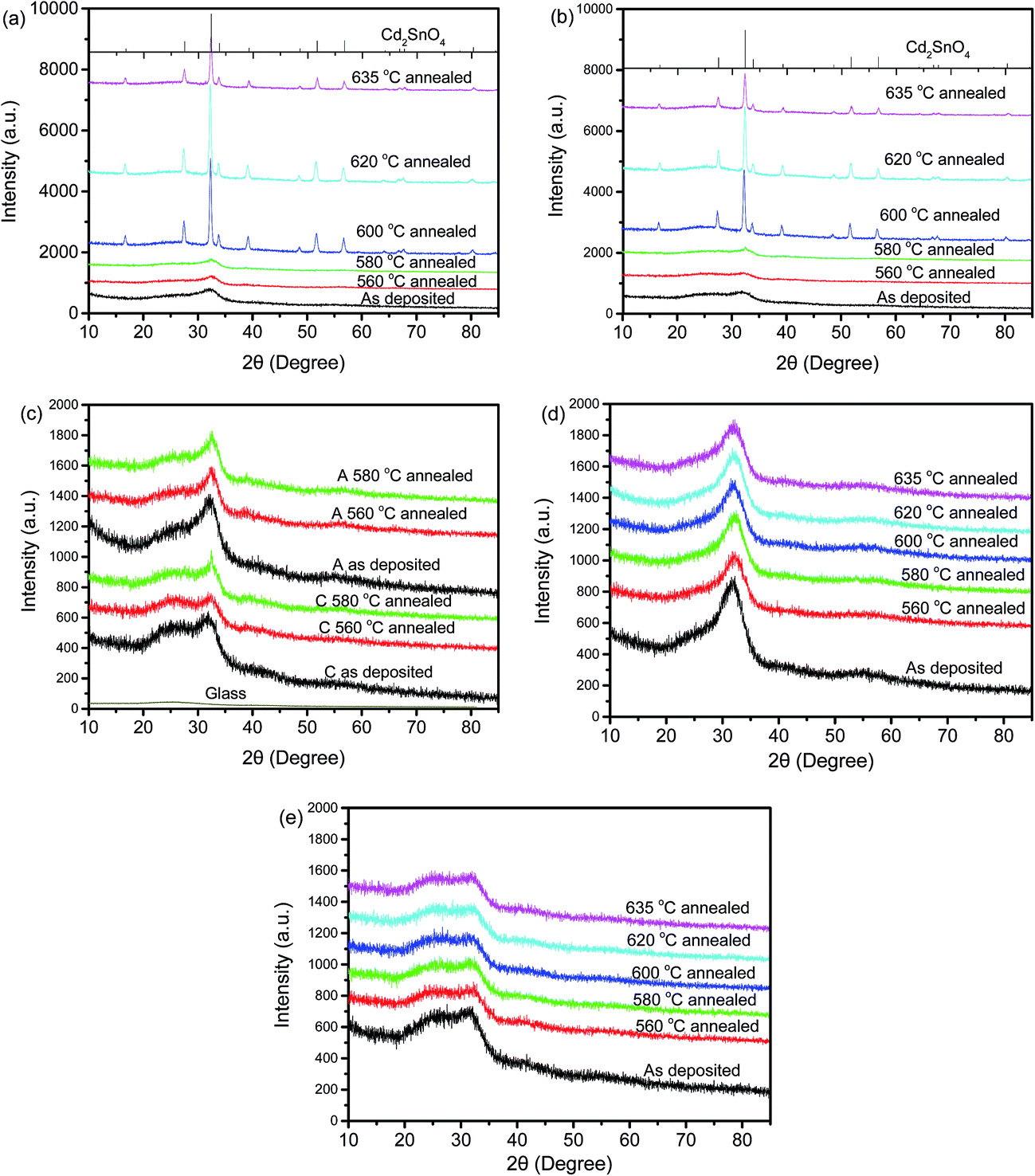 | ||
| Fig. 1 XRD patterns of some samples: (a) sample A (Ar/O2 atmosphere deposited, 388 nm), (b) sample C (Ar/O2 atmosphere deposited, 172 nm), (c) low temperature annealed samples A and C, (d) sample A′ (Ar atmosphere deposited, 627 nm) and (e) sample C′ (Ar atmosphere deposited, 210 nm). | ||
| Annealing atmosphere | Annealing temperature (°C) | Lowest resistivity (Ω cm) | Reference |
|---|---|---|---|
| Ar | 400–500 | ∼10−4 | 3 |
| Ar | 500 | 1.74 × 10⁻⁴ | 4 |
| Ar/CdS | 600–700 | 1.54 × 10⁻⁴ | 5 |
| Ar, Ar/CdS | 580–700 | 1.28 × 10⁻⁴ (adapted to world record CdTe cell) | 7 |
| Ar/CdS | 450–700 | 1.6 × 10⁻⁴ | 8 |
| He, H2 | 500–700 | 2.07 × 10⁻⁴ | 9 |
| Air | 600 | ∼6.6 × 10⁻² | 10 |
| He/CdS, low pressure | 650, 700 | 1.9 × 10⁻⁴ | 11 |
| CdS | 600 | 2.8 × 10⁻⁴ | 12 |
| N2 | 600–635 | 1.73 × 10⁻⁴ | This work |
In summary, the as-deposited Cd2SnO4 films are amorphous, whether sputtered in pure Ar or in an Ar/O2 atmosphere. Cd2SnO4 sputtered in an atmosphere containing 20% O2 crystallises after annealing in N2 at a temperature above 600 °C. In addition, the crystalline state is similar between the annealing temperature of 600 °C and 635 °C. Thus, in this case, formation of Cd2SnO4 requires O2 both in the sputtering atmosphere and the post deposition annealing at a temperature of at least 600 °C in an N2 atmosphere. Mainly because of the lack of O atoms, the Ar atmosphere sputtered CTO film cannot form a Cd2SnO4 phase after annealing.
3.2 Electrical properties
Fig. 2 shows the electrical property variation of Cd2SnO4 samples with annealing at various temperatures of 560 °C, 580 °C, 600 °C, 620 °C and 635 °C. The insets of Fig. 2a and b show the resistivity. Meanwhile, the insets in Fig. 2c and d show the carrier mobility, whereas the insets of Fig. 2e and f show carrier concentration. | ||
| Fig. 2 Properties of annealed samples: (a) resistivity of Ar/O2 atmosphere deposited films; (b) resistivity of Ar atmosphere deposited films; (c) carrier mobility of Ar/O2 atmosphere deposited films; (d) carrier mobility of Ar atmosphere deposited films; (e) carrier concentration of Ar/O2 atmosphere deposited films; (f) carrier concentration of Ar atmosphere deposited films. | ||
When the deposition atmosphere contains 20% of oxygen, all the as-grown Cd2SnO4 films exhibited high resistivity at a magnitude of 10−1 Ω cm. These CTO films are not suitable for use as a transparent conductive oxide (TCO) electrode of thin film solar cells. For example, at a carrier mobility of 19.1 cm2 V−1 s−1 and carrier concentration of 9.0 × 1017 cm−3, sample A shows a resistivity of 0.363 Ω cm (more detailed information about the as-deposited films is given in Table 1 in the Appendix†).
As shown in Fig. 2a, the resistivity of all the films sputtered in Ar/O2 dropped drastically to 10−4 Ω cm after annealing in N2. The resistivity decreased with an increase of the annealing temperature, and reached a minimum during annealing at 620 °C for all the four films with different thicknesses. The conductivity of thinner films [C (172 nm) and D (142 nm)] was obviously better than that of thicker samples [A (388 nm) and B (348 nm)] during annealing at a relatively low temperature of 560 °C and 580 °C. Resistivity of C and D is already approximately 4 × 10⁻⁴ Ω cm after the low temperature annealing at 560 °C and 580 °C. However, their sheet resistance is above 20 Ω sq−1. This result is not suitable for their use as TCO for thin film solar cells. However, the difference of resistivity decreased during annealing at high temperatures between 600 °C and 635 °C.
Sample D has resistivity of 1.73 × 10⁻⁴ Ω cm after annealing at a temperature of 620 °C. This value is the lowest resistivity achieved in this research. Even though sample D is the thinnest of the four samples, its sheet resistance is still as low as 12.21 Ω sq−1 after annealing in N2 at 620 °C (Appendix Table 5†). This result is similar to that obtained using commercial fluorine doped SnO2 with a thickness between 350 nm and 500 nm. After the same annealing process, thick CTO films were found to exhibit low sheet resistance down to 5.07 Ω sq−1 (sample A, 388 nm) and similar resistivity below 1.97 × 10⁻⁴ Ω cm. Therefore, in terms of its electrical properties, adopting an ultrathin CTO of 172 nm and 142 nm as a transparent front electrode of a thin film solar cells is acceptable. Obviously, sputtering in an O2 containing atmosphere and post deposition annealing in N2 at a temperature above 600 °C are the two significant requirements for achieving such a low resistivity and feasible sheet resistance for thin film solar cells.
For CTO sputtered without O2, the resistivity of the as-deposited films is already as low as 10−4 Ω cm. For example, sample A′ (627 nm) exhibited an as-deposited resistivity of 6.14 × 10⁻⁴ Ω cm, a carrier mobility of 26.4 cm2 V−1 s−1 and a carrier concentration of 2.85 × 1020 cm−3. However, these as-deposited films are not transparent as will be discussed later. After annealing, the resistivity of these films was ramped up, increasing in the order of magnitude of 10−2 Ω cm for thick films [sample A′ (627 nm) and B′ (420 nm)]. Resistivity also increased with annealing temperature. For thin films, the resistivity of samples C′ (210 nm) and D′ (150 nm) remains, even lower than that of the as-deposited ones. Resistivity of annealed samples C′ and D′ is mostly between 4 and 8 × 10⁻⁴ Ω cm. However, the sheet resistance is higher than 30 Ω sq−1. Sheet resistance of annealed thick samples [A′ (627 nm) and B′ (420 nm)] is higher than 400 Ω sq−1. All these results show that these samples are too resistive for use as thin film solar cells. Thus, in terms of its electrical property, CTO sputtered without O2 is not a good candidate for thin film solar cells, whether as-deposited or annealed.
Fig. 2c and d show the carrier mobility of films sputtered in Ar/O2 and Ar, respectively. Except for sample A, carrier mobility of films sputtered in Ar/O2 is higher than 20 cm2 V−1 s−1 after annealing and reaches a maximum (49.7 cm2 V−1 s−1) at an annealing temperature of 620 °C. For films sputtered without O2, the carrier mobility after annealing exhibits a strong dependence on thickness, i.e., the thicker the film, the lower the carrier mobility. Carrier mobility of annealed samples [A′ (627 nm) and B′ (420 nm)] are lower than 2.5 cm2 V−1 s−1. However, the carrier mobility of thin films [annealed samples C′ (210 nm) and D′ (150 nm)] are one order of magnitude higher than that of samples A′ and B′. Variation of carrier mobility of films sputtered without O2 is less than one order of magnitude for annealing between 560 °C and 635 °C.
Fig. 2e and f show the carrier concentration of annealed CTO deposited in Ar/O2 and a pure Ar atmosphere, respectively. Carrier concentrations of CTO films sputtered in Ar/O2 are mostly at the high end of 1020 cm−3 after the annealing and increased with the annealing temperature until 620 °C was reached. After annealing at 620 °C, the carrier concentration of all these films reached a maximum above 6 × 1020 cm−3. For CTO films sputtered without O2, the carrier concentrations were all at the low end of 1020 cm−3 and only changed slightly with annealing temperature, i.e., mostly between 1.6 × 1020 cm−3 and 2.4 × 1020 cm−3. Briefly, the high conductivity of CTO films sputtered in Ar/O2 and annealing in N2 above 620 °C is ascribed to high carrier mobility above 40 cm2 V−1 s−1 as well as high carrier concentration of high 1020 cm−3.
After annealing at a temperature of 620 °C, the resistivity of the thinnest CTO film deposited (sample D) in Ar/O2 (Ar/O2 = 8/2) exhibited the lowest resistivity of 1.73 × 10⁻⁴ Ω cm, which corresponded to a carrier mobility of 43.7 cm2 V−1 s−1 and a carrier concentration of 8.25 × 1020 cm−3. The resistivity of the N2 atmosphere annealed CTO films was also quite low compared with the resistivity of CTO films annealed in an atmosphere of Ar, Ar/CdS, He and H2. The thickness of sample D was only 142 nm and it took 17 min for deposition (8.35 nm min−1). Compared with other annealing atmospheres, N2 is less expensive and can reduce manufacturing costs in the mass production of CTO films.
The figures in Table 1 compare the lowest resistivity of CTO films after annealing in various atmospheres. More detailed information about the deposition and annealing of CTO films is listed in Table 7 (see the Appendix†). Table 1 shows that CTO film annealed in a N2 atmosphere exhibited the lowest resistivity of all the CTO films annealed without the presence of CdS. This result suggests that the N2 atmosphere annealing process of CTO film could be added into existing CdTe thin film photovoltaic (PV) module manufacturing lines and run independently to all other processes.
Free carriers in Cd2SnO4 can be generated from the ionisation of O vacancies (Ov), cadmium interstitials (Cdi)2,6,15 or both.6 In cadmium rich CTO films, the SnCd antisite defect is the donor.16 When the deposition atmosphere contains O2, enough O2 atoms exist to react with Cd and Sn atoms, creating compounds, such as CdO, SnO2, CdSnO3 and Cd2SnO4, with less O vacancies, Cdi and SnCd. However, carrier concentration of the as-deposited CTO films is low and this is because of the amorphous state of the as-deposited film. After annealing in a N2 atmosphere, the crystallinity of the CTO sputtered in the O2 containing atmosphere increased, thus, improving the carrier mobility. Meanwhile, some O2 atoms may leave the films, creating more carriers. When the annealing temperature was relatively low, the O atoms in the thicker samples could not effectively diffuse out. Therefore, the carrier concentration of the Ar/O2 gas sputtered thicker CTO films was relatively low. For the CTO films sputtered in pure Ar, more Ov and Cdi can be observed because of lack of O2 in the deposition atmosphere. This phenomenon results in high carrier concentration. The dependence of carrier mobility on the annealing temperature and film thickness for CTO films sputtered in a pure Ar atmosphere needs further study.
3.3 Optical properties
When sputtered in pure Ar, the thick CTO films were dark coloured and the thin ones were light dark coloured. Meanwhile, the colour of the thick CTO films were yellow, and that of the thin ones was light yellow when sputtered in an Ar/O2 mixture. All the films became crystal clear after annealing at a temperature of 600 °C or higher. Fig. 3 shows the transmittance curves of these films.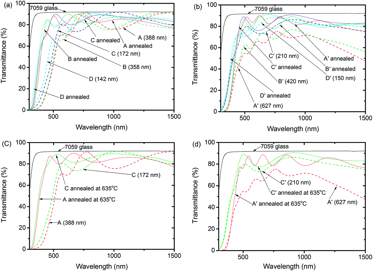 | ||
| Fig. 3 Transmittance curves of some CTO films before and after annealing: (a) curves of deposited films A, B, C and D in an Ar/O2 atmosphere, at annealing temperature of 620 °C; (b) curves of deposited films A′, B′, C′ and D′ in an Ar atmosphere at an annealing temperature of 620 °C; (c) curves of deposited films A and C in an Ar/O2 atmosphere at an annealing temperature of 635 °C; (d) curves of deposited films A′ and C′ in an Ar atmosphere at an annealing temperature of 635 °C. | ||
Fig. 3a shows that the transmittance of the CTO films improves significantly after annealing when sputtered in an atmosphere containing O2. Transmittance in the short wave region increased obviously while maintaining high transmittance in long wave region. A blue shift obviously exists for the absorption edge of films sputtered in Ar/O2 after annealing at 620 °C in N2. This shift is further reinforced after annealing at 635 °C (Fig. 3c). The absorption edge shift of Ar/O2 sputtered films is mainly ascribed to band gap enlargement, as shown in Fig. 4a. The increase of band gap is because of the Burstein–Moss effect.17–19 The difference of the transmittance at short wavelength in these samples is ascribed to film thickness.
 | ||
| Fig. 4 Relation between (hνα)2 and (hν): (a) sample A (deposited in an Ar/O2 atmosphere at 388 nm at an annealing temperature of 620 °C); (b) sample A′ (deposited in an Ar atmosphere at 627 nm at an annealing temperature of 620 °C). | ||
As shown in Fig. 3b and d, the short wave region transmittance of pure Ar sputtered films increased after annealing at 620 °C and 635 °C, and this is similar to the effect of long wave region transmittance. Fig. 3b and d also show that the absorption edge does not shift after annealing when compared with the as-deposited films. The difference of the transmittance at a short wavelength for these samples is also ascribed to film thickness.
The optical band gap of CTO films can be extracted according to curves describing the relationship between (hνα)2 and (hν),20–22 where h is the Planck's constant, ν is frequency of incident photons and α is the absorption coefficient. Fig. 4 shows (hνα)2 curves of Ar/O2 sputtered sample A and pure Ar sputtered sample A′, before and after annealing. As shown in Fig. 4a, the band gap of the as-deposited CTO sputtered in Ar/O2, i.e., sample A, is 2.83 eV and this increases to 3.38 eV after annealing at 620 °C. Fig. 4b shows that the optical band gap of the as-deposited CTO sputtered in pure Ar, i.e., film A′, is 3.32 eV, which did not change after annealing at 620 °C. The increased optical band gap of the Ar/O2 sputtered CTO films after annealing is beneficial for thin film solar cells because when the CTO films act as a transparent conductive layer, more short wave light can be transmitted into the absorption layer of the solar cells, increasing the short wave current of the solar cells.
Table 2 lists the average transmittance, average reflectance and average absorption of CTO films on a Corning 7059 glass between wavelengths of 400 nm and 900 nm before and after annealing at 620 °C. The average transmittance between a wavelength of 400 nm and 900 nm of all the as-deposited films is below 80% and this is also correlated to film thickness, however, it increases to above 80% after annealing. Variation of transmittance between CTO with different thicknesses decreases. This result demonstrated that the annealing process improves the transmittance of all the CTO films. Transmittance increase is ascribed to a reduction of absorption as the reflectance of the annealed films did not obviously change. The absorption of thin Ar/O2 atmosphere deposited samples [C (172 nm) and D (142 nm)] is as low as 0.19% and 0.04%, respectively. This result indicates that the transmittance of visible light can be enhanced very close to 100% by simply applying antireflection (AR) layers on the other side of the CTO. CTOs with an absorption of 0.19% and 0.04% together with an AR coating can result in negligible optical loss for solar cell applications. Therefore, in terms of both electrical and optical properties, annealing is beneficial to Ar/O2 sputtered CTO films.
| Deposition atmosphere | Sample | Thickness (nm) | T (%) | R (%) | A (%) | |||
|---|---|---|---|---|---|---|---|---|
| As-deposited | Annealed | As-deposited | Annealed | As-deposited | Annealed | |||
| Ar + O2 | A | 388 | 66.50 | 82.53 | 15.78 | 16.09 | 17.72 | 1.38 |
| B | 358 | 66.37 | 82.54 | 16.68 | 16.82 | 16.95 | 0.64 | |
| C | 172 | 68.16 | 83.05 | 19.56 | 16.76 | 12.28 | 0.19 | |
| D | 142 | 73.48 | 85.56 | 16.94 | 14.40 | 9.58 | 0.04 | |
| Ar | A′ | 627 | 62.01 | 82.11 | 13.20 | 12.73 | 24.79 | 5.16 |
| B′ | 420 | 65.17 | 79.56 | 13.92 | 17.31 | 20.91 | 3.13 | |
| C′ | 210 | 76.30 | 81.51 | 15.90 | 17.54 | 7.80 | 0.95 | |
| D′ | 150 | 80.18 | 83.03 | 15.04 | 16.63 | 4.78 | 0.34 | |
3.4 Robustness
Chloride treatment is crucial for the CdTe solar cells. In solar cells with a superstructure structure, the TCO layer is deposited before the CdTe absorber. Thus, the TCO layer goes through high temperature chloride treatment together with the absorber. To evaluate the robustness of the N2 atmosphere annealed CTO films during chloride treatment, N2 atmosphere annealed samples A (388 nm, sputtered in Ar/O2 gas) and C (172 nm, sputtered in Ar/O2 gas) were treated a dry air/CdCl2 atmosphere at 400 °C for 60 min, and these were labelled as ‘2nd chloride treatment’. The detailed configuration was similar to that of chloride treatment to a conventional CdTe thin film solar cell, which is described elsewhere in the literature.23 To simulate the annealing procedure of ‘TCO/CdS/CdTe’ in real solar cells, a 200 nm CdS film on 7059 glass was also used as proximity cap.24 The electrical properties of CTO samples A and C are plotted in Fig. 5. For comparison, the properties of N2 treated samples A and C are also plotted, and labelled as ‘1st N2 treatment’. The 2nd chloride treatment actually caused the electrical properties of samples A and C to deteriorate if the CTO film went through the 1st N2 treatment at 560 °C and 580 °C. However, when the 1st N2 treatment temperature is 600 °C or higher, the resistivity of the CTO films was insignificantly increased during the 2nd chloride treatment. Although the carrier concentration decreased during the 2nd chloride treatment, the carrier mobility remains the same or even increases. This result demonstrated that the electrical properties of CTO post N2 annealing at high temperature resilient to the standard chloride treatment of the CdTe-based solar cell. The detailed electrical properties of samples A and C after the 2nd chloride treatment are listed in Table 8 in the Appendix.† During the 2nd treatment in the air/CdCl2 atmosphere, some O atoms diffused into the CTO film, filling the O vacancies and reacting with the cadmium interstitials. This reaction might decrease the donor concentration of the CTO film, and the 2nd chloride treatment might increase the crystallinity of the CTO film, thus, increasing the carrier mobility.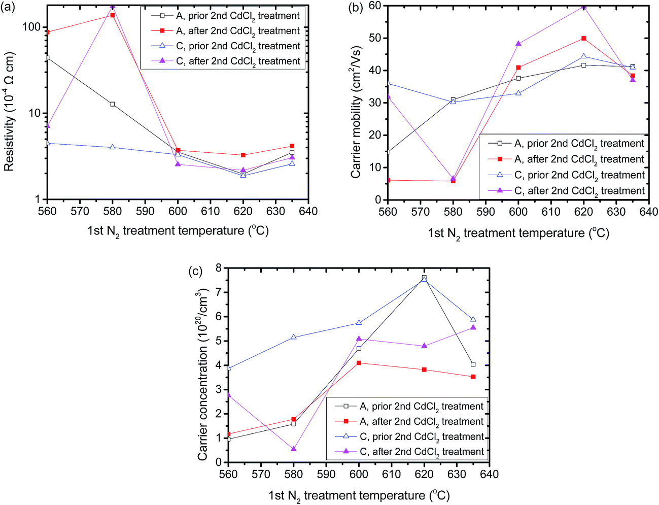 | ||
| Fig. 5 Electrical properties of N2 gas annealed samples A and C before and after chloride treatment, where (a) is the resistivity, (b) is the carrier mobility and (c) is the carrier concentration. | ||
For the same reason, TCO also goes through a high temperature vacuum procedure if it is used for the high temperature CdTe deposition technique, such as closed space sublimation (CSS) and vapour transport deposition (VTD). Sample C (172 nm, sputtered in Ar/O2 gas) was annealed in a vacuum (p = 6 × 10⁻⁴ Pa) at 600 °C for 5 min. This film was annealed in a N2 atmosphere at 620 °C for 30 min before the vacuum annealing. The resistivity, carrier mobility and carrier concentration of the vacuum annealed CTO sample C were 1.83 × 10⁻⁴ Ω cm, 51.8 cm2 V−1 s−1 and 6.60 × 1020 cm−3, respectively. Its resistivity was 1.88 × 10⁻⁴ Ω cm before vacuum annealing. This finding demonstrated the robustness, to the vacuum high temperature process, of the Ar/O2 sputtered and N2 annealed CTO films.
To evaluate the robustness to acidic etching, the Ar/O2 sputtered and N2 annealed CTO films were placed into a 2.38 mol L−1 hydrochloric acid solution for 5 min and a 2.00 mol L−1 sulfuric acid (H2SO4) solution for 5 min, respectively, and no etching was detected. Furthermore, no electrical property change occurred. This demonstrated that the CTO film is resilient to etching with strong acids.
The fabrication process of high quality CTO films as indicated by this work is potentially adaptable to existing CdTe PV manufacturing lines of high temperature techniques, such as CSS and VTD. This result can be considered from two aspects. Firstly, no CdS is required in the annealing process to achieve high conductivity. Secondly, the electrical properties of CTO after the annealing in N2 were found to be resilient to the secondary high temperature processes and acidic etching in strong acid. These features make it feasible to adapt the CTO sputtering and annealing process to existing manufacturing lines, thus, causing no change to existing processes.
4. Conclusion
Annealing in N2 gas cannot decrease resistivity of films deposited in an Ar atmosphere. The CTO films sputtered in pure Ar gas were amorphous, and the optical band gap did not largely change after annealing, although the transmittance increased.As far as is known, in this research, magnetron sputtered CTO films have been annealed in N2 gas for the first time. CTO films sputtered in Ar/O2 mixed gas were crystallised after annealing in N2 at 600 °C or higher than 600 °C for 30 min. Annealing in N2 drastically increased carrier mobility and carrier concentration of such CTO films, decreasing the resistivity to a value as low as 1.73 × 10⁻⁴ Ω cm. Annealing in N2 also enhanced the transmittance of such CTO films and enlarged the optical band gap. This research demonstrated that annealing in N2 of oxygenised CTO film can achieve electrical and optical properties similar to or better than those of CTO films annealed in an atmosphere of Ar, Ar/CdS, He or H2. Furthermore, because N2 is abundant, annealing CTO films with it can reduce the manufacturing cost of mass production high quality CTO film. Through modulating the deposition parameters and annealing parameters, the electrical and optical properties of CTO films annealed in a N2 atmosphere can be improved further. The CTO films deposited in an Ar/O2 atmosphere after which they were annealed in N2 gas are resilient to a second annealing process, such as chloride treatment and vacuum annealing. This condition makes it suitable for use in high temperature CdTe thin film solar cell manufacturing technology.
Acknowledgements
This work was supported by the National High Technology Research and Development Program of China (No. 2015AA050609), the National Natural Science Foundation of China (No. 61274060), and the Chinese Academy of Sciences Interdisciplinary Innovation Team.References
- X. Wu, Sol. Energy, 2004, 77, 803–814 CrossRef CAS.
- A. J. Nozik, Phys. Rev. B: Solid State, 1972, 6, 453–459 CrossRef CAS.
- W. L. Wang, K. J. Liao, C. Z. Cai, G. B. Liu and Y. Ma, Surf. Coat. Technol., 2003, 167, 284–287 CrossRef CAS.
- P. Dongliang, J. Shengrui and W. Wanlu, Chin. Phys. Lett., 1993, 10, 189–192 CrossRef.
- G. Haacke, Appl. Phys. Lett., 1976, 28, 622 CrossRef CAS.
- G. Haacke, W. E. Mealmaker and L. A. Siegel, Thin Solid Films, 1978, 55, 67–81 CrossRef CAS.
- X. Wu, W. P. Mulligan and T. J. Courts, Thin Solid Films, 1996, 286, 274–276 CrossRef CAS.
- T. Meng, B. McCandless, W. Buchanan, E. Kimberly and R. Birkmire, J. Alloys Compd., 2013, 556, 39–44 CrossRef CAS.
- R. Mamazza Jr, D. L. Morel and C. S. Ferekides, Thin Solid Films, 2005, 484, 26–33 CrossRef.
- S.-H. Lee, E.-W. Lee, S.-Y. Park and C.-W. Jeon, Mol. Cryst. Liq. Cryst., 2010, 532, 106 Search PubMed.
- D. M. Meysing, J. M. Burst, W. L. Rance, M. O. Reese, T. M. Barnes, T. A. Gessert and C. A. Wolden, Sol. Energy Mater. Sol. Cells, 2013, 117, 300–305 CrossRef CAS.
- J. A. Stoke, J. D. Beach, W. C. Bradford and T. R. Ohno, Thin Solid Films, 2014, 562, 254–259 CrossRef CAS.
- F. Golestani, T. Hashemi, K. J. D. Mackenzie and C. A. Hogarth, J. Mater. Sci., 1983, 18, 3679–3685 CrossRef.
- http://psec.uchicago.edu/glass/Corning7059Properties.pdf(20160330).
- T. Stapiński, E. Leja and T. Pisarkiewicz, J. Phys. D: Appl. Phys., 1984, 17, 407–413 CrossRef.
- S. B. Zhano and Su-H. Wei, Appl. Phys. Lett., 2002, 80, 1376–1378 CrossRef.
- R. Wen, L. Wang, X. Wang, G.-H. Yue, Y. Chen and D.-L. Peng, J. Alloys Compd., 2010, 508, 370–374 CrossRef CAS.
- B.-Y. Oh, M.-C. Jeong, D.-S. Kim, W. Lee and J.-M. Myoung, J. Cryst. Growth, 2005, 281, 475–480 CrossRef CAS.
- B. L. Zhu, K. Li, J. Wang, J. Wu, D. W. Zeng and C. S. Xie, Superlattices Microstruct., 2013, 64, 460–469 CrossRef CAS.
- J. Tauc, R. Grigorovici and A. Vancu, Phys. Status Solidi B, 1966, 15, 627–637 CrossRef CAS.
- J. Mass, P. Bhattacharya and R. S. Katiyar, Mater. Sci. Eng., B, 2003, 103, 9–15 CrossRef.
- F. Z. Tepehan, F. E. Ghodsi, N. Ozer and G. G. Tepehan, Sol. Energy Mater. Sol. Cells, 1999, 59, 265–275 CrossRef CAS.
- H. Li and X. Liu, Sol. Energy, 2015, 115, 603–612 CrossRef CAS.
- Z. Du, X. Liu, Y. Zhang, J. Shuai and H. Li, RSC Adv., 2016, 6, 108067–108074 RSC.
Footnote |
| † Electronic supplementary information (ESI) available. See DOI: 10.1039/c7ra00394c |
| This journal is © The Royal Society of Chemistry 2017 |