
 Open Access Article
 This Open Access Article is licensed under a
 Creative Commons Attribution 3.0 Unported Licence
Synthesis and highly effective purification of silver nanowires to enhance transmittance at low sheet resistance with simple polyol and scalable selective precipitation method†
Molla Bahiru Gebeyehu,
Tolesa Fita Chala ,
Shao-Yen Chang,
Chang-Mou Wu and
Jiunn-Yih Lee*
,
Shao-Yen Chang,
Chang-Mou Wu and
Jiunn-Yih Lee*
Department of Materials Science and Engineering, National Taiwan University of Science and Technology, Taipei 10607, Taiwan, Republic of China. E-mail: jlee@mail.ntust.edu.tw; Fax: +886-2-27376519
First published on 13th March 2017
Abstract
Networks of metal nanowires (NWs) have the highest performance of any solution-coatable material to replace expensive indium tin oxide (ITO) as the transparent conducting electrode material in next-generation devices. However, there is as yet no published process for producing NW films with an optoelectronic performance that exceeds that of ITO. Here, we examine a process for the synthesis and purification of uniform AgNWs that, when coated using a spin-coating technique to create a transparent conducting film, show properties that exceed those of ITO. The morphology AgNWs can be controlled by adjusting the concentration of silver nitrate (AgNO3) and [PVP] to [AgNO3] molar ratio. AgNWs with average diameters of 20 nm and aspect ratios >1000 were obtained by adding 30.5 mM of AgNO3 and 6![[thin space (1/6-em)]](https://www.rsc.org/images/entities/char_2009.gif) :1 molar ratio of [PVP] to [AgNO3] in a silver nanowire synthesis, but these NWs were contaminated by some Ag nanoparticles. Selective precipitation was used to purify the NWs from nanoparticles, resulting in a transmittance improvement as large as 2%. The transmittance of the purified AgNW film was 97.5% at a sheet resistance of below 70 Ω sq−1. The synthesized and purified AgNWs were analyzed by field-emission scanning electron microscopy (FE-SEM), atomic force microscopy (AFM), transmission electron microscopy (TEM), energy dispersive spectroscopy (EDS), energy dispersive X-ray spectroscopy (EDX), X-ray diffraction (XRD), X-ray photoelectron spectroscopy (XPS), ultraviolet-visible-near-infrared (UV-Vis-NIR) spectroscopy and four-point-probe technique.
:1 molar ratio of [PVP] to [AgNO3] in a silver nanowire synthesis, but these NWs were contaminated by some Ag nanoparticles. Selective precipitation was used to purify the NWs from nanoparticles, resulting in a transmittance improvement as large as 2%. The transmittance of the purified AgNW film was 97.5% at a sheet resistance of below 70 Ω sq−1. The synthesized and purified AgNWs were analyzed by field-emission scanning electron microscopy (FE-SEM), atomic force microscopy (AFM), transmission electron microscopy (TEM), energy dispersive spectroscopy (EDS), energy dispersive X-ray spectroscopy (EDX), X-ray diffraction (XRD), X-ray photoelectron spectroscopy (XPS), ultraviolet-visible-near-infrared (UV-Vis-NIR) spectroscopy and four-point-probe technique.
Introduction
One-dimensional nanostructures of metals play an important role as both active components and interconnects in fabricating nanoscale electronic devices for a large number of optoelectronic applications.1 Transparent conductive films are broadly used in components of optoelectronic devices in liquid crystal displays, large-area touch screens, thin-film solar cells, electromagnetic shielding, organic light emitting diodes and photovoltaic devices.2–9 Currently, many transparent conductive films are made of a sputtered film of indium tin oxide (ITO) due to its high transmittance at low sheet resistances.10–12 However, the high-conductivity ITO used in these applications is particularly brittle and highly expensive because of the slow coating rates involved with sputtering. This has inspired the search for solution-coatable alternatives to ITO that can be coated at high speeds and give comparable performance. There are various solution-coatable alternatives to ITO, including ultra-thin metallic films,13–16 metallic mesh-structures,17–19 conducting polymers and their hybrids,20–24 graphene,25–31 carbon nanotubes,32–36 silver nanowires (AgNWs),37–39 and copper nanowires (CuNWs).40–42 Nevertheless, only commercially available AgNWs have a verified optoelectronic performance that exceeds that of ITO.43 The processes important for the production of metal NWs that, when coated onto a substrate, have optoelectronic performance exceeding that of ITO have not been reported. The performance of AgNW-based transparent conductors generally increases with decreasing diameter and increasing NW aspect ratio. Thus, thin NWs scatter less light and increasing aspect ratio reduces the number of high-resistance NW–NW contacts in a film.44–46 Numerous methods for the synthesis of AgNWs have been developed. These methods include chemical synthesis,47–49 hydrothermal method,50–52 electrochemical technique,53,54 ultraviolet irradiation photodetection technique,55,56 DNA template,57,58 porous materials template,59,60 coaxial electro-spinning61 and polyol process,49,62,63 but none have demonstrated film performance that exceeds that of ITO.5,38,64 When these methods are compared in terms of simplicity and cost effectiveness, the polyol process seems to be the most promising one.65 AgNWs with a mean diameter of 20 nm and lengths up to 20 μm were prepared by a high-pressure polyol method.38 These NWs were used to produce films with a sheet resistance of 40 Ω sq−1 at a transmittance of 88%, performance below that of ITO. Lee and co-workers have developed a successive multistep growth process to obtain AgNWs with an average diameter of 160 nm and length of 95.1 μm. Though such long NWs exhibited optoelectronic performance exceeding that of shorter NWs, their diameters are too large to match the properties of ITO.39 Thus, there remains a need for a synthesis of AgNWs that are both very ultra-thin (∼20 nm in average diameter) and very long (>40 μm in length) so as to achieve ITO-level performance. However, it is not enough to obtain AgNWs with precise dimensions; they must also be very pure and uncontaminated by the existence of nanoparticles. These nanoparticle impurities dramatically decrease the electrical conductivity and transparency of NW networks.66,67 Given the fact that the polyol synthesis is the most popular and versatile method used for the production of AgNWs with inevitable nanoparticles as a side product, this remains an important issue for the synthesis of high-purity AgNWs.38,64,68,69 The old-fashioned purification process of performing many tedious cycles of centrifugation is time-consuming and some authors have not produced AgNWs with sufficient purity.37,68 Pradel and co-workers developed a cross-flow filtration method to purify NWs, but the success of this method depends on many parameters, such as NW pore size of the fiber membrane, flow rate, and pressure, and is not easily scalable.66 Thus, there remains a need for a simple, convenient, cost-effective and scalable method for separating nanoparticles from NWs. Many research groups have explored different approaches in order to improve the polyol process. There are also numerous reports in the literature that focus on the effect of different parameters on the polyol synthesis of AgNWs.70–72 However, in these studies, only a few parameters of the polyol process have been examined.Herein, we demonstrate simple polyol method and scalable selective precipitation for the synthesis of well dispersed, highly purified, ultra-thin, large-scale, uniform AgNWs to make high-performance optically transparent conducting films, which have a lower sheet resistance than that obtained with CNT and ITO and comparable to the values previously obtained using AgNWs. In this method, poly(vinylpyrrolidone) (PVP) was used as stabilizing and capping agent combined with sodium chloride (NaCl) and potassium bromide (KBr) salts, ethylene glycol (EG) was used as both solvent and a reducing agent, and silver nitrate (AgNO3) was used as a silver precursor.63 We also determined that the diameter and uniformity of AgNWs can be controlled by adjusting the concentration of AgNO3 and [PVP] to [AgNO3] molar ratio keeping the other parameters constant. AgNWs with diameters of 20 nm and aspect ratios >1000 were obtained by adding 30.5 mM AgNO3 to a silver nanowire synthesis. Moreover, we purified AgNWs from unwanted nanoparticles with a simple selective precipitation process. Finally, the purified and prepared AgNW ink was coated with spin-coating methods onto a glass substrate to produce films with an average transmittance of 97.5% at a sheet resistance of below 70 Ω sq−1.
Experimental section
Materials
PVP (K-90, MW = 1300000, Sigma-Aldrich, USA), silver nitrate (AgNO3, Sigma-Aldrich, UK), sodium chloride and potassium bromide (NaCl and KBr, Sigma-Aldrich Co. Ltd, USA), EG (Sigma-Aldrich, USA) and ethanol (CH3CH2OH, Sigma-Aldrich, USA) were used for AgNW synthesis without further purification. All glassware used in the experiments was cleaned with deionized water, acetone (99.8%), isopropyl alcohol (99.8%) and finally deionized water.
Synthesis of AgNWs
The AgNWs were synthesized with a simple polyol method.72,73 In a standard synthesis, different concentration of AgNO3 (i.e. 20.6, 30.5, 60.4 and 90.3 mM), 3.5 mM NaCl and 1.8 mM KBr solutions in EG were prepared as six separate solutions at room temperature, while 75 mg of PVP was dissolved in 10 mL of EG (contained in a 100 mL vial) and heated in an oil bath at 160 °C for 60 min under magnetic stirring (550 rpm). Then, 40 μL of NaCl and 20 μL of the KBr solution were pipetted into the vial. After 20–30 min, 5.2 mL of the AgNO3 solution was continuously added through a syringe pump at an injection rate of 0.2 mL min−1. After injection of silver nitrate solution, the reaction mixture was further refluxed at 160 °C for 3 h until the color of the solution became white to gray as shown schematically in Fig. 1A. During the heating process, nitrogen gas was bubbled through the reaction solution. Magnetic stirring was continuously applied throughout the entire process of reduction of silver ions and wire growth. After 3 h, the solution-containing bottle was removed from the oil bath and the turbid polyol solution was air cooled to room temperature, thereby quenching the reaction.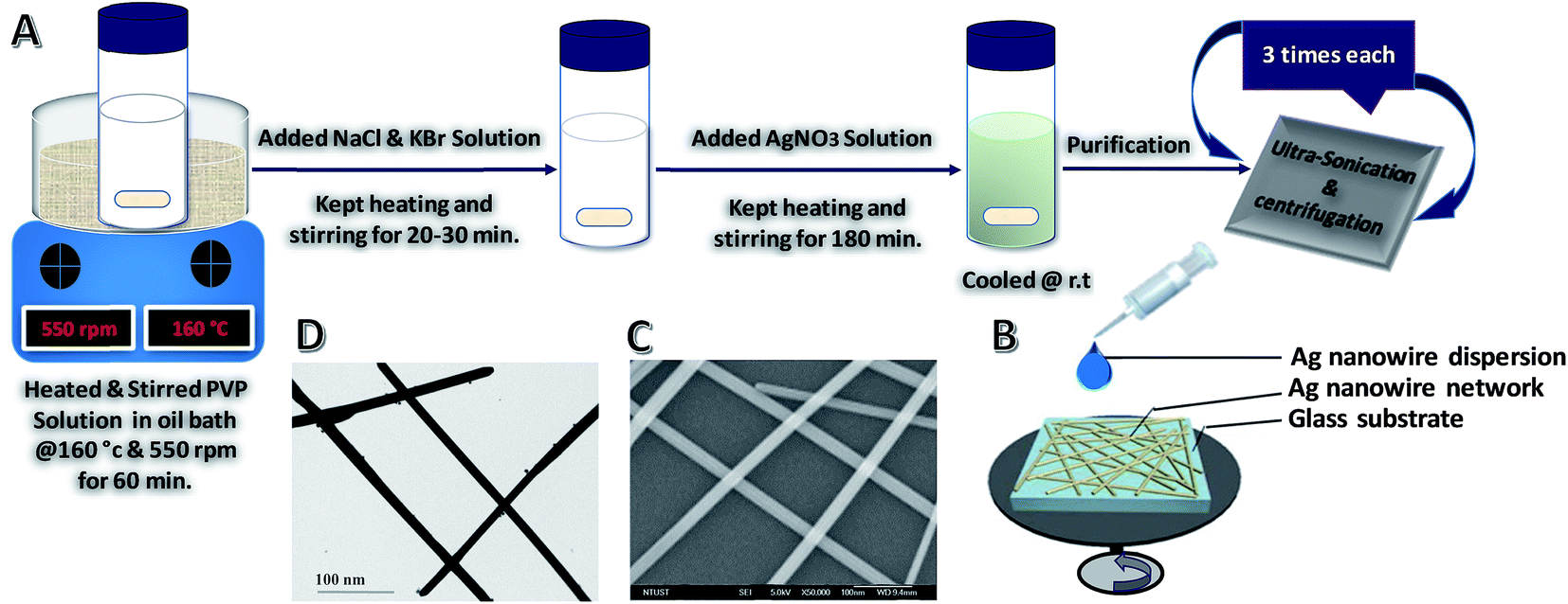 | ||
| Fig. 1 (A) Schematic diagram of synthesis and purification of AgNWs with polyol process at 160 °C for 3 h. (B) Schematic diagram of spin-coated AgNW network on a glass substrate. (C) FE-SEM image of the spin-coated AgNW network on the glass substrate. (D) TEM image of the spin-coated AgNW network on a lacey carbon-coated copper grid. | ||
After the synthesis, the resulting AgNWs could be purified and separated from nanoparticles through ultrasonication and centrifugation processes (Fig. 1A). In this case, the reaction mixture was diluted with acetone (6–10 times by volume) for ultrasonication and centrifuged at 5000 rpm for 10 min. The supernatant silver nanoparticles could be easily removed using a pipette. The aggregated NWs were dispersed in 10 mL of ethanol. Subsequently, the re-dispersed NWs were purified again by adding 10–20 mL of acetone, allowing the NWs to settle for 5 min, and removing the supernatant. The ultrasonication and centrifugation procedures were repeated three times until the supernatant became colorless. Every time before centrifugation to remove the PVP polymer layer, the wires were shaken gently to prevent them from breaking down. NWs with high purity were obtained after 2–3 cycles of this purification protocol. The final purified and precipitated product was dispersed in ethanol for further characterization.
Fabrication of transparent conducting AgNW films
Transparent conductive films were made in a manner similar to that of previous reports.40,74 The purified AgNWs were transferred into an ink containing ethyl alcohol, ethyl cellulose, ethyl acetate, pentyl acetate, isopropyl alcohol and toluene for use with a spin-coating method. Briefly, the ink formulation was prepared by dissolving ethyl cellulose (0.05 g) in ethyl alcohol (3.0 g), before addition of ethyl acetate (0.25 g), pentyl acetate (0.4 g), isopropanol (0.5 g), and toluene (1.15 g). After the AgNWs were washed with ethyl alcohol, the ink formulation (1.2 mL) was added to the AgNWs, and this suspension was vortexed. The dispersion was centrifuged at a low speed (∼500 rpm) so that a well-dispersed AgNW ink could be pipetted from the solution. To make conductive films, microscope glass slides with dimensions of 25 × 75 × 1.0 mm were purchased from Fisher Scientific and cut into pieces with dimensions of 25 × 50 × 1.0 mm. These slides were thoroughly cleaned with detergent and washed with deionized water, sonicated in acetone, isopropanol, and ethanol each for 5 minutes and dried in an oven. A transparent conductive film of AgNW ink was prepared by spin-coating the AgNW ink dispersion at 500 rpm on the surface of the glass substrate. In the spin-coating process, 60 μL NW ink was spread on the glass substrate with waiting for 30 seconds before spinning to let the nanowires reach near the glass surface; to enhance the evaporation rate, methanol was added to the glass substrate and well agitated. Different densities of NW ink on the surface of the glass substrate were obtained by varying the concentration of the NWs. The slides coated with AgNW ink were dried in air for 10 minutes at 70 °C. Once the slides returned to room temperature, they were dipped in a mixture of ethyl alcohol and acetone (3:1, v/v) for 15 seconds to remove the organic material and dried under nitrogen gas. Finally, the slides were put into a 70 °C oven in air for 20 minutes. The transmittance and sheet resistance of each NW film were measured using a UV-Vis-NIR spectrophotometer and a four-point probe.
Characterization
The morphologies of NWs were investigated using field-emission scanning electron microscopy (FE-SEM, JSM 6500F, JEOL), high-resolution transmission electron microscopy (HR-TEM, H-7000, Hitachi) and atomic force microscopy (AFM, Bruker Dimension ICON). The crystalline structure of AgNW mesh was characterized by a Bruker D2-phase diffractometer using Cu Kα radiation (λ = 1.5418 Å) in the range of 20–80° (2θ). The elemental composition and binding energy of the core electronic state were characterized by energy dispersive spectroscopy (EDS/FE-SEM, JSM 6500F, JEOL), energy dispersive X-ray spectroscopy (EDX/TEM, H-7000, Hitachi) and X-ray photoelectron spectroscopy (XPS) (VG-ESCA, British Thermo Scientific, Theta Probe). Furthermore, the optical properties (absorption and transmittance spectra) and sheet resistance of each NW film were measured using a Jasco V-670 UV-visible-near-infrared (UV-Vis-NIR) spectrometer and four-point-probe technique (Keith Link Technology, Taiwan).Results and discussion
Purification of AgNWs
Nanoparticles and other low-aspect-ratio shapes are a common byproduct from the solution chemical growth of NWs.75 They are formed because growth is diffusion-limited and nucleation is not instantaneous, thus causing nanoparticles to grow along multiple pathways. These undesirable nanoparticles can bring much difficulty to the subsequent material processing steps and degrade the material performance in device applications. For example, the presence of these short nanoparticles greatly affects the assembly of the NWs. When making one-dimensional arrays of NWs, the byproduct particles act as structural defects, disrupting the packing of the NWs.76 Even a small number of nanoparticles can prevent the formation of a one-dimensional lattice. Also, as many properties of nanoparticles are highly shape- and size-dependent,77 such byproducts can have a detrimental effect on the quality of the final NW material. For example, AgNWs have rapidly attracted attention as an alternative material to ITO for making high-quality transparent conductor thin films.5,78,79 Although there has been a great success in the synthesis of AgNWs, predominantly by the polyol route,1 the product is often contaminated by low-aspect-ratio particles and rods. The presence of these nanoparticle impurities in the NW network is highly undesirable because they would only have a marginal involvement in the electrical conductivity as they are too small to provide effective current pathways, but they will cause significant optical loss owing to their stronger light scattering properties.80 As the commercial production of AgNW transparent conductors has emerged,78 there is a pressing requirement for a purification route that can meet the industrial scale of synthesis. Nanoparticle purification can be accomplished utilizing basic laboratory separation techniques, such as simple filtration, dialysis, and gel electrophoresis. However, these approaches are generally limited to small-scale processing and are time-consuming. There are the additional challenges of protecting the NWs from deformation under the applied force field and keeping them dispersed in the solvent after the sedimentation steps during processing. For example, gel electrophoresis is capable of separating nanoparticle solutions by shape and size with great precision,81 but the materials need to be first processed through the gel, and then exchanged to an appropriate solvent, making it difficult to maintain the colloidal stability of the NWs except at low concentrations. Dialysis is non-destructive but needs an extended processing time as determined by the diffusion rate of nanoparticles across the permeable membrane. Furthermore, most dialyzing membranes are designed to eliminate sub-10 nm substances, such as polymer chains, small molecules, and viruses, thus limiting their use for NW purification. Simple filtration (i.e., dead-end filtration) is routinely applied to remove small particles from NW samples by passing the dispersion through size-selection membranes. The downward solvent flow could easily damage the NWs, especially those caught lying across the membrane pores. Another common challenge is the reduction of retention and flow rate of nanoparticle impurities by the filter cake. However, centrifugation is an effective and convenient NW purification process in large-scale production, a non-destructive, scalable method. This allows the production of uniform, ultra-thin and high-aspect-ratio NWs for optoelectronic application in general.Fig. 2 shows SEM images of AgNWs with diameters of 22 ± 2 nm and lengths of 50 ± 5 μm before and after three cycles of selective precipitation (see Fig. S1 in ESI† for SEM images of before and after 1st, 2nd and 3rd cycle of purification). There is visibly a dramatic decrease in the number of particles and organic phase after the purification process.
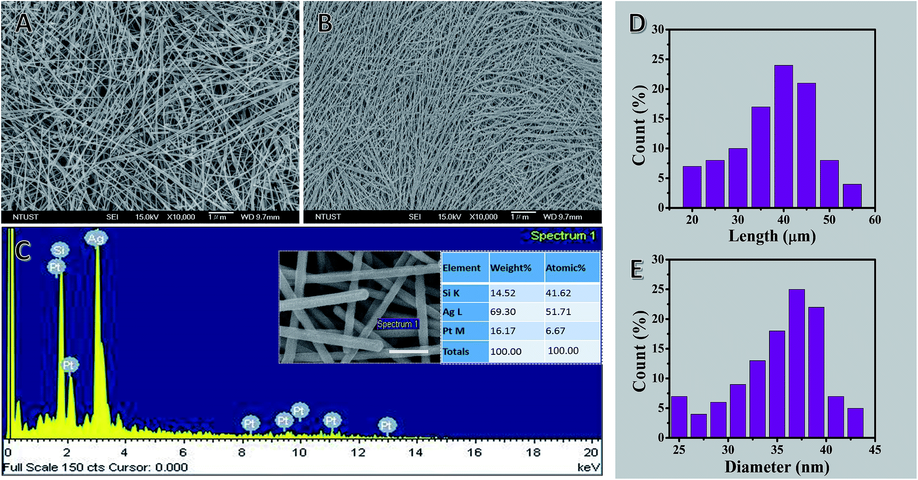 | ||
| Fig. 2 Morphological and elemental composition characterization of uniform, ultra-thin, purified and large-scale AgNWs prepared by the polyol method at 160 °C and atmospheric pressure for 3 h of reaction. FE-SEM images (A) before purification and (B) after purification. (C) EDS spectrum of the corresponding inset image. The inset image in (C) shows a high-magnification FE-SEM image of purified AgNWs on 100 nm scale. The inset table in spectrum (C) shows the elemental composition of the sample surface. (D and E) Histograms showing the distribution of NW lengths and diameters after purification respectively. | ||
The EDS spectrum and tabulated results revealed that Ag, Si, and Pt are the main elements present with Ag being the most abundant in the selected field. The Ag peaks originate from the precursor (AgNO3), whereas Si peaks originate from the glass slide that supports the sample and Pt is present due to the sputtering step for sample preparation for SEM imaging. In addition, C, O, N, Na, K, Br and Cl peaks do not appear in the EDS spectrum of the sample mats, which further supports that the AgNWs were highly purified from the precursor materials, such as polymer, salt, and solvent. Moreover, the tabulated results provide a quantitative view of the elemental composition in the inspection area in units of both weight percent and atomic percent.
Effects of AgNO3 concentration on the morphology of AgNWs
AgNO3 acts as the precursor, and its concentration is vital to the yield and morphology of AgNWs because it can expand the preparation scale and change the aspect of AgNWs.82,83 In this study, we varied the concentration of AgNO3 added to the synthesis to gain additional insight into how it affects NW diameter and purity; all the other parameters in the typical polyol process are kept constant. The FE-SEM (A–D) and TEM (E–H) images of the AgNWs synthesized at different AgNO3 concentrations are shown in Fig. 3. It can be seen that AgNWs tend to become shorter and wider as the concentration of AgNO3 increases, which is consistent with what is reported elsewhere.84 In addition, when the concentration of AgNO3 is too high or too low, the numbers of nanoparticles increase substantially, as shown from corresponding FE-SEM and TEM images in Fig. 3. Briefly, when there was only 20.6 mM of AgNO3 present in the polyol synthesis, it produced non-uniform AgNWs with a mean diameter of 29 ± 11 nm and lengths of 32 ± 7 μm (Fig. 3A and E); whereas when there was only 30.5 mM of AgNO3 present in the polyol synthesis, it produced uniform AgNWs with a mean diameter of 22 ± 2 nm and lengths of 50 ± 5 μm (Fig. 3B and F). The addition of 60.4 mM AgNO3 into the AgNW synthesis produced a mixture of nanoparticles and NWs with an average diameter of 35 ± 10 nm and lengths of 25 ± 15 μm (Fig. 3C and G). Further increasing the concentration of AgNO3 to 90.3 mM resulted in much more nanoparticles in the reaction product (Fig. 3D and H). Our experimental results show that, when AgNO3 at a high concentration was added, the silver ion concentration was high in a volume of the same unit, causing the possibility of molecular collisions to increase. Consequently, the chemical reaction rate increased, and Ag nanoparticles were synthesized at larger sizes. The added capping agent (PVP) can cover the synthesized Ag nanoparticles.85 The capped coating was arranged along one dimension to form many Ag nanoparticles and a small number of AgNWs having large diameters (low aspect ratios), as shown in Fig. 3D and H. In contrast, adding a low concentration of AgNO3 led to the synthesis of AgNWs with small diameters (high aspect ratios), as shown in Fig. 3B and F. Particularly, when the AgNO3 concentration is 30.5 mM, uniform NWs, and least byproducts, are produced. Thus, we selected 30.5 mM as the optimal concentration of AgNO3.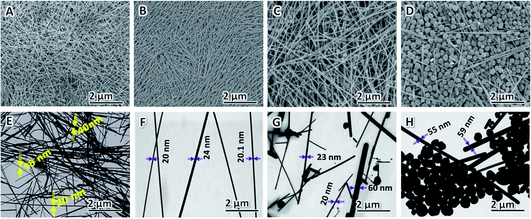 | ||
| Fig. 3 FE-SEM (A–D) and TEM (E–H) images of purified products obtained from different concentrations of AgNO3: (A and E) 20.6, (B and F) 30.5, (C and G) 60.4 and (D and H) 90.3 mM respectively, while the other all parameters were kept constant. | ||
Effects of [PVP] to [AgNO3] molar ratio on morphology of AgNWs
Xia et al. verified that the anisotropic growth of AgNWs is maintained by selectively covering the facets with PVP while leaving some of the facets largely uncovered by PVP and thus highly reactive. The final morphologies of AgNWs at the end of the polyol process are strongly dependent on the [PVP] to [AgNO3] molar ratio86 and the molecular weight of PVP chain.87,88 The effect of [PVP] to [AgNO3] molar ratio on the morphology of AgNWs is shown in Fig. 4A–F. When the [PVP] to [AgNO3] molar ratio is too small, the as-prepared AgNWs have non-uniform morphology, and low aspect ratio is obtained since the planes cannot be adequately passivated.89 When the [PVP] to [AgNO3] molar ratio is too large, more Ag nanoparticles and very much fewer AgNWs are obtained, because in this case90 the planes are completely passivated (Fig. 4F). Therefore, in order to obtain AgNWs with the least by-products, uniform morphology, and large aspect ratio, we selected the optimal [PVP] to [AgNO3] molar ratio as 6:1.
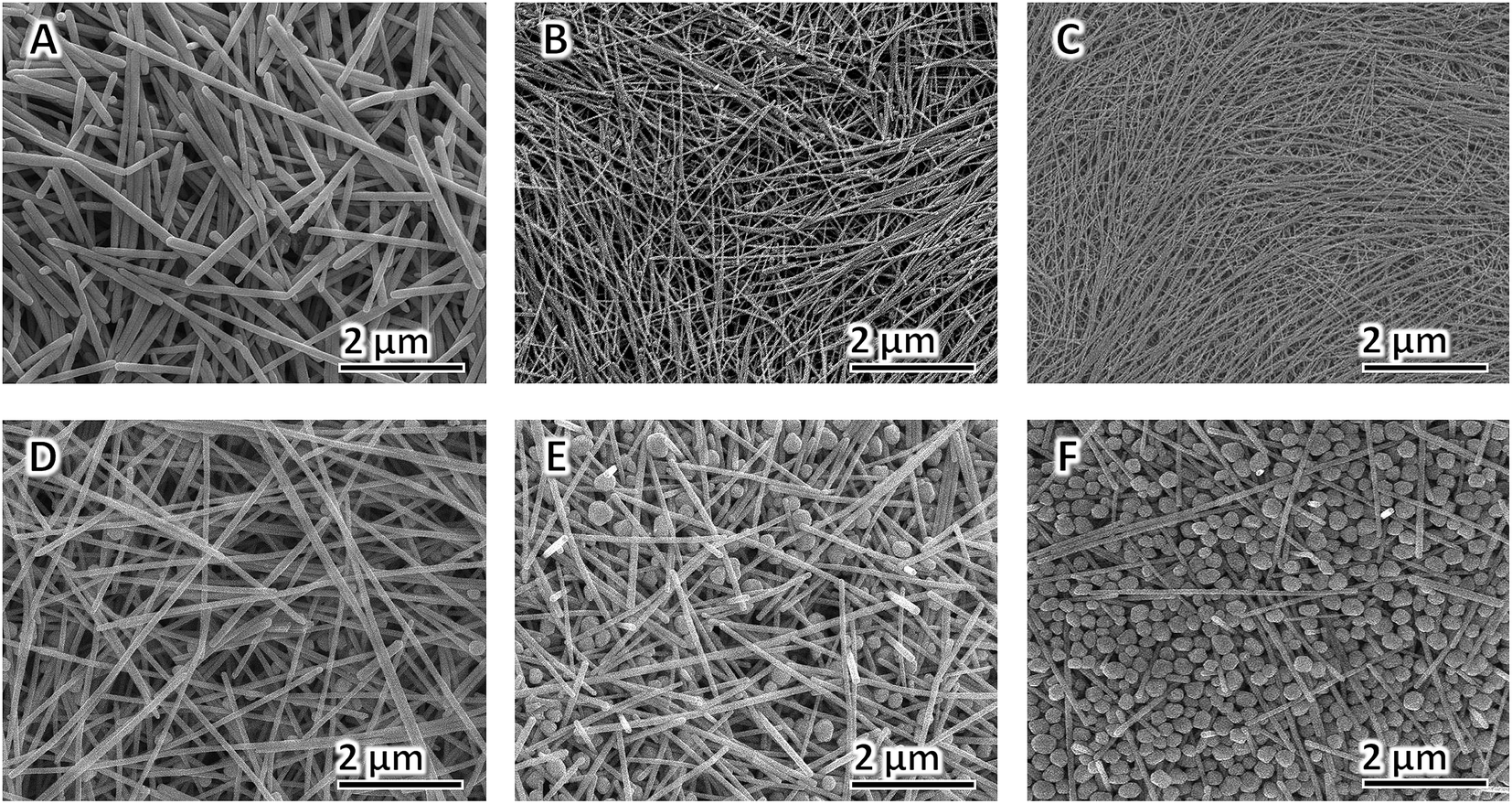 | ||
| Fig. 4 FE-SEM images of AgNWs synthesized at different [PVP] to [AgNO3] molar ratio: (A) 2:1, (B) 4:1, (C) 6:1, (D) 8:1, (E) 10:1, and (F) 12:1. | ||
The XRD pattern of purified AgNWs is shown in Fig. 5A. This shows four peaks, which are located at diffraction angles 2θ = 38.2° (111), 2θ = 44.4° (200), 2θ = 64.4° (220), and 2θ = 77.6° (311). Based on the experimental data, the synthesized and purified AgNW diffraction peaks can be indexed to face-centered cubic with a lattice constant of about 4.085 Å, which is very close to the reported value (α = 4.082 Å, JCPDS file no. 04-0783). The intensity ratio of the reflections at (111) and (200) exhibits a high value indicating that (111) is the preferred coordination similar to previous reports.51,91
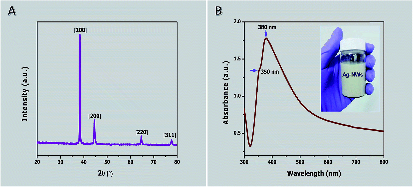 | ||
| Fig. 5 (A) XRD pattern of the purified as-prepared AgNWs (160 °C; 3 h) indicating FCC crystals. (B) UV-visible absorption spectrum of the purified AgNWs. The inset in (B) shows a photo of AgNW solution, dispersed in ethanol after purification. | ||
The UV-visible absorption spectrum after three cycles of ultrasonication, centrifugation and separation of the product obtained at 1 h is shown in Fig. 5B (see Fig. S2 in ESI† for before and after purification). In this case, the precipitate indicates a typical UV-Vis spectrum of pure AgNWs in ethanol solution. The absorption spectrum exhibits two relatively sharp surface plasmon resonance peaks at about 350 and 380 nm. The absorption peak at 350 nm could be attributed to the plasmon response of long AgNWs, similar to that of bulk silver, whereas the peak at 380 nm may be assigned to the transverse plasmon mode of AgNWs.91 A peak at 410 nm corresponding to silver nanoparticles is detected in the spectrum before purification (see Fig. S2 in ESI†). The absence of the peak allocated to silver nanoparticles indicates the purity of the AgNWs because of the effective removal of silver nanoparticles.
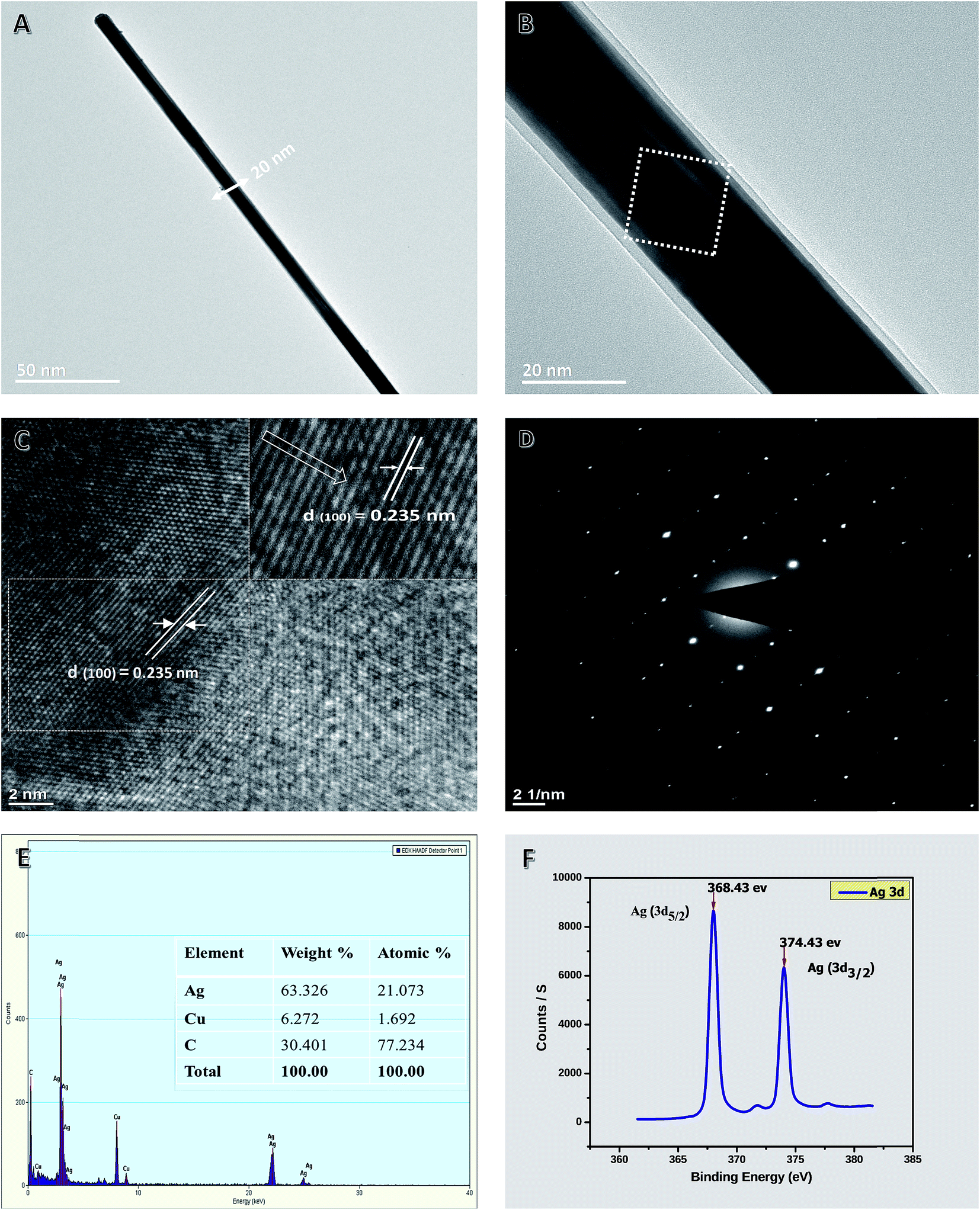
Fig. 6A shows a single representative of purified AgNWs with a diameter of 20 nm. Fig. 6B shows a high-resolution TEM image of an AgNW. It shows that there is a twin plane located parallel to the AgNW longitudinal axis, and the spacings of the lattice planes at symmetrical twin boundaries are both 2.35 Å, which is consistent with the standard (111) crystal spaces (JCPDS file no. 04-0783). Fig. 6C shows the lattice fringes of a single AgNW of the selected dashed square area in Fig. 6B. The pattern clearly shows that there is only a set of the diffraction pattern, indicating the selected area is a single-crystal NW. The calculated spacing distance was 2.35 Å, which corresponds to (111) and further confirmed the plane of metallic silver. The chemical compositions of AgNWs were determined by EDX analysis of samples deposited on a lacey carbon-coated copper grid. The EDX spectrum (Fig. 6E) shows the presence of Ag element, in which the peaks of the corresponding Ag element were distinct (other peaks originated from the copper and carbon from the TEM grid). The XPS spectrum in the region of Ag 3d of purified AgNWs is shown in Fig. 6F. The resulting NWs show two peaks centered at 368.43 and 374.43 eV, corresponding to Ag 3d5/2 and 3d3/2 binding energy, respectively, with a spin–orbit separation of 6.00 eV, which are consistent with previously reported values (368.48 and 374.48 eV) for Ag dendrites.92
 | ||
| Fig. 6 Typical structural and morphological characterization of AgNWs. (A) TEM image of single NW with a diameter of 20 nm. (B) TEM image of single NW at high magnification. (C) HR-TEM image shows the lattice fringes in the middle region of a single AgNW. The calculated spacing distance is indexed to face centered cubic silver. The lattice fringes confirm the crystalline structure. The big white arrow in inset image of (C) indicates the twin boundary of the NW. (D) Selected area electron diffraction (SAED) of a single AgNW. (E) TEM/EDX spectrum analysis of AgNWs. (F) The Ag 3d XPS spectrum of purified AgNWs. | ||
Further, surface roughness and topography studies were also conducted by AFM as shown in Fig. 7. The root mean surface (RMS) roughness of a representative single AgNW on glass is 2.5 nm, indicating a much-enhanced surface smoothness of the AgNW on the glass substrate compared to that of a previous report.93 Fig. 7A and B show the AFM image of AgNWs in different views, whereas Fig. 7C shows the corresponding line scan data of AgNWs.
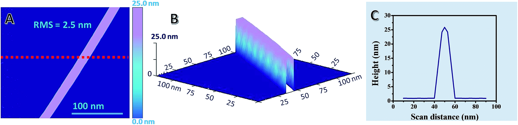 | ||
| Fig. 7 Morphological characterization and analysis of a representative single AgNW on a glass surface in different views: (A) 2D AFM image and (B) 3D AFM image. (C) The representative line scan data corresponding to the red dashed line in (A). | ||
Fig. 8A shows an FE-SEM image of a spin-coated AgNW film. Fig. 8B shows a plot of specular transmittance (% T) versus sheet resistance (Rs) for films of AgNWs of ∼20 nm in diameter before and after purification, together with some of the best previous literature results for solution-coatable transparent conductors. The transmittance of films made from purified NWs was up to 2% greater than that of films made from NWs without purification. The performance of the purified NWs exceeds the performance of any other unpurified transparent conductor at sheet resistances >45 Ω sq−1. Only AgNWs from Cambrios have higher values at lower sheet resistance. These results further demonstrate the importance of the aspect ratio, diameter, and purity for the performance of NW-based transparent conductors.
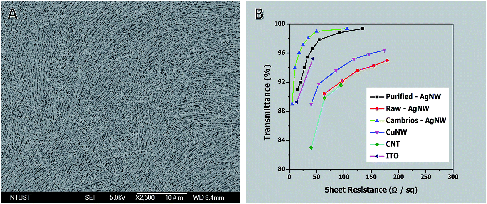 | ||
| Fig. 8 (A) Typical FE-SEM image of AgNW film. (B) A plot of specular transmittance (λ = 550 nm) versus sheet resistance for AgNW films before and after purification. Each data point is the average of five measurements. The performances of AgNWs,42 CuNWs,94 CNT,95 and ITO are shown for comparison. | ||
Conclusions
The main goal of this study proposes to enhance the transmission of synthesized AgNW films at low sheet resistance with a simple and scalable selective precipitation process. In addition to that, we also studied the effect of AgNO3 concentration and [PVP] to [AgNO3] molar ratio on the formation of ultrathin, very long and uniform AgNWs. The results indicate that AgNWs with small diameter (∼20 nm) and high aspect ratios (>1000) were produced when the concentration of AgNO3 and [PVP] to [AgNO3] molar ratio were 30.5 mM and 6:1 respectively. The reduction in NW diameter obtained through the optimization of AgNO3 concentration was primarily due to an increase in the number of nucleation events, and secondly due to a reduction in the percentage conversion of Ag+ to Ag0. The nanoparticles that undoubtedly contaminate the NWs produced by the polyol synthesis can be removed with a simple and scalable selective precipitation process. The purified and prepared AgNW ink with high aspect ratio NWs was then uniformly coated onto glass substrates with a spin-coating technique to make transparent conducting films. These transparent conducting films exhibited an average transmittance of 97.5% at a sheet resistance of below 70 Ω sq−1. The purification of the NWs enhanced the transmittance at a given sheet resistance by as much as 2%. Different kinds of selective precipitation process can likely enable the purification of a wide variety of NWs. The synthesis of uniform NWs and purification process demonstrated here are suggested to be very useful for researchers in industry standard and academia seeking to produce NW-based films with a performance that exceeds that of ITO.
Acknowledgements
This study was supported by Ministry of Science and Technology of the Republic of China under grant MOST 103-2218-E-011-007.References
- Y. Sun, B. Gates, B. Mayers and Y. Xia, Nano Lett., 2002, 2, 165–168 CrossRef CAS.
- F. Qian, S. Gradecak, Y. Li, C.-Y. Wen and C. M. Lieber, Nano Lett., 2005, 5, 2287–2291 CrossRef CAS PubMed.
- Y. Hu, Y. Zhang, C. Xu, G. Zhu and Z. L. Wang, Nano Lett., 2010, 10, 5025–5031 CrossRef CAS PubMed.
- D. Zhang, K. Ryu, X. Liu, E. Polikarpov, J. Ly, M. E. Tompson and C. Zhou, Nano Lett., 2006, 6, 1880–1886 CrossRef CAS PubMed.
- L. Hu, H. S. Kim, J.-Y. Lee, P. Peumans and Y. Cui, ACS Nano, 2010, 4, 2955–2963 CrossRef CAS PubMed.
- K. S. Leschkies, R. Divakar, J. Basu, E. Enache-Pommer, J. E. Boercker, C. B. Carter, U. R. Kortshagen, D. J. Norris and E. S. Aydil, Nano Lett., 2007, 7, 1793–1798 CrossRef CAS PubMed.
- F. Bonaccorso, Z. Sun, T. Hasan and A. Ferrari, Nat. Photonics, 2010, 4, 611–622 CrossRef CAS.
- X. Wang, L. Zhi and K. Müllen, Nano Lett., 2008, 8, 323–327 CrossRef CAS PubMed.
- D. Zhang, R. Wang, M. Wen, D. Weng, X. Cui, J. Sun, H. Li and Y. Lu, J. Am. Chem. Soc., 2012, 134, 14283–14286 CrossRef CAS PubMed.
- Z. Chen, W. Li, R. Li, Y. Zhang, G. Xu and H. Cheng, Langmuir, 2013, 29, 13836–13842 CrossRef CAS PubMed.
- J. Lee, M. A. Petruska and S. Sun, J. Phys. Chem. C, 2014, 118, 12017–12021 CAS.
- J. Lee, S. Lee, G. Li, M. A. Petruska, D. C. Paine and S. Sun, J. Am. Chem. Soc., 2012, 134, 13410–13414 CrossRef CAS PubMed.
- J. Zou, C. Z. Li, C. Y. Chang, H. L. Yip and A. K. Y. Jen, Adv. Mater., 2014, 26, 3618–3623 CrossRef CAS PubMed.
- J. H. Kim, P. W. Liang, S. T. Williams, N. Cho, C. C. Chueh, M. S. Glaz and A. K. Y. Jen, Adv. Mater., 2015, 27(4), 695–701 CrossRef CAS PubMed.
- D. Gu, C. Zhang, Y.-K. Wu and L. J. Guo, ACS Nano, 2014, 8, 10343–10351 CrossRef CAS PubMed.
- B. Bari, J. Lee, T. Jang, P. Won, S. H. Ko, K. Alamgir, M. Arshad and L. J. Guo, J. Mater. Chem. A, 2016, 4, 11365–11371 CAS.
- P. Kuang, J. M. Park, W. Leung, R. C. Mahadevapuram, K. S. Nalwa, T. G. Kim, S. Chaudhary, K. M. Ho and K. Constant, Adv. Mater., 2011, 23, 2469–2473 CrossRef CAS PubMed.
- L. Hu, H. Wu and Y. Cui, MRS Bull., 2011, 36, 760–765 CrossRef CAS.
- B. O'Connor, C. Haughn, K.-H. An, K. P. Pipe and M. Shtein, Appl. Phys. Lett., 2008, 93, 223304 CrossRef.
- P. Lee, J. Ham, J. Lee, S. Hong, S. Han, Y. D. Suh, S. E. Lee, J. Yeo, S. S. Lee and D. Lee, Adv. Funct. Mater., 2014, 24, 5671–5678 CrossRef CAS.
- J. Lee, P. Lee, H. B. Lee, S. Hong, I. Lee, J. Yeo, S. S. Lee, T. S. Kim, D. Lee and S. H. Ko, Adv. Funct. Mater., 2013, 23, 4171–4176 CrossRef CAS.
- D. Y. Choi, H. W. Kang, H. J. Sung and S. S. Kim, Nanoscale, 2013, 5, 977–983 RSC.
- L. Yang, T. Zhang, H. Zhou, S. C. Price, B. J. Wiley and W. You, ACS Appl. Mater. Interfaces, 2011, 3, 4075–4084 CAS.
- A. Elschner and W. Lövenich, MRS Bull., 2011, 36, 794–798 CrossRef CAS.
- J. H. Lee, D. W. Shin, V. G. Makotchenko, A. S. Nazarov, V. E. Fedorov, Y. H. Kim, J. Y. Choi, J. M. Kim and J. B. Yoo, Adv. Mater., 2009, 21, 4383–4387 CrossRef CAS PubMed.
- J. K. Wassei and R. B. Kaner, Mater. Today, 2010, 13, 52–59 CrossRef CAS.
- L. Gomez De Arco, Y. Zhang, C. W. Schlenker, K. Ryu, M. E. Thompson and C. Zhou, ACS Nano, 2010, 4, 2865–2873 CrossRef CAS PubMed.
- M.-S. Lee, K. Lee, S.-Y. Kim, H. Lee, J. Park, K.-H. Choi, H.-K. Kim, D.-G. Kim, D.-Y. Lee and S. Nam, Nano Lett., 2013, 13, 2814–2821 CrossRef CAS PubMed.
- S. Bae, H. Kim, Y. Lee, X. Xu, J.-S. Park, Y. Zheng, J. Balakrishnan, T. Lei, H. R. Kim and Y. I. Song, Nat. Nanotechnol., 2010, 5, 574–578 CrossRef CAS PubMed.
- K. S. Kim, Y. Zhao, H. Jang, S. Y. Lee, J. M. Kim, K. S. Kim, J.-H. Ahn, P. Kim, J.-Y. Choi and B. H. Hong, Nature, 2009, 457, 706–710 CrossRef CAS PubMed.
- Y. Zhu, Z. Sun, Z. Yan, Z. Jin and J. M. Tour, ACS Nano, 2011, 5, 6472–6479 CrossRef CAS PubMed.
- K.-Y. Chun, Y. Oh, J. Rho, J.-H. Ahn, Y.-J. Kim, H. R. Choi and S. Baik, Nat. Nanotechnol., 2010, 5, 853–857 CrossRef CAS PubMed.
- A. Du Pasquier, H. E. Unalan, A. Kanwal, S. Miller and M. Chhowalla, Appl. Phys. Lett., 2005, 87, 203511 CrossRef.
- A. Kumar and C. Zhou, ACS Nano, 2010, 4, 11–14 CrossRef CAS PubMed.
- J. U. Park, M. Meitl, S. H. Hur, M. L. Usrey, M. S. Strano, P. J. Kenis and J. A. Rogers, Angew. Chem., 2006, 118, 595–599 CrossRef.
- H.-Z. Geng, K. K. Kim, K. P. So, Y. S. Lee, Y. Chang and Y. H. Lee, J. Am. Chem. Soc., 2007, 129, 7758–7759 CrossRef CAS PubMed.
- C. Mayousse, C. Celle, E. Moreau, J.-F. Mainguet, A. Carella and J.-P. Simonato, Nanotechnology, 2013, 24, 215501 CrossRef PubMed.
- E.-J. Lee, M.-H. Chang, Y.-S. Kim and J.-Y. Kim, APL Mater., 2013, 1, 042118 CrossRef.
- J. Lee, P. Lee, H. Lee, D. Lee, S. S. Lee and S. H. Ko, Nanoscale, 2012, 4, 6408–6414 RSC.
- A. R. Rathmell, S. M. Bergin, Y. L. Hua, Z. Y. Li and B. J. Wiley, Adv. Mater., 2010, 22, 3558–3563 CrossRef CAS PubMed.
- H. Guo, N. Lin, Y. Chen, Z. Wang, Q. Xie, T. Zheng and D. L. Peng, Sci. Rep., 2013, 3, 2323 Search PubMed.
- S. Ye, A. R. Rathmell, Z. Chen, I. E. Stewart and B. J. Wiley, Adv. Mater., 2014, 26, 6670–6687 CrossRef CAS PubMed.
- S. I. Na, S. S. Kim, J. Jo and D. Y. Kim, Adv. Mater., 2008, 20, 4061–4067 CrossRef CAS.
- S. M. Bergin, Y.-H. Chen, A. R. Rathmell, P. Charbonneau, Z.-Y. Li and B. J. Wiley, Nanoscale, 2012, 4, 1996–2004 RSC.
- R. M. Mutiso, M. C. Sherrott, A. R. Rathmell, B. J. Wiley and K. I. Winey, ACS Nano, 2013, 7, 7654–7663 CrossRef CAS PubMed.
- S. De, P. J. King, P. E. Lyons, U. Khan and J. N. Coleman, ACS Nano, 2010, 4, 7064–7072 CrossRef CAS PubMed.
- N. R. Jana, L. Gearheart and C. J. Murphy, Chem. Commun., 2001, 617–618 RSC.
- S. H. Kim, B. S. Choi, K. Kang, Y.-S. Choi and S. I. Yang, J. Alloys Compd., 2007, 433, 261–264 CrossRef CAS.
- S. Coskun, B. Aksoy and H. E. Unalan, Cryst. Growth Des., 2011, 11, 4963–4969 CAS.
- J. Xu, J. Hu, C. Peng, H. Liu and Y. Hu, J. Colloid Interface Sci., 2006, 298, 689–693 CrossRef CAS PubMed.
- Z. Wang, J. Liu, X. Chen, J. Wan and Y. Qian, Chem.–Eur. J., 2005, 11, 160–163 CrossRef PubMed.
- Z. Yang, H. Qian, H. Chen and J. N. Anker, J. Colloid Interface Sci., 2010, 352, 285–291 CrossRef CAS PubMed.
- L. Huang, H. Wang, Z. Wang, A. Mitra, K. N. Bozhilov and Y. Yan, Adv. Mater., 2002, 14, 61 CrossRef CAS.
- M. Mazur, Electrochem. Commun., 2004, 6, 400–403 CrossRef CAS.
- Y. Zhou, S. H. Yu, C. Y. Wang, X. G. Li, Y. R. Zhu and Z. Y. Chen, Adv. Mater., 1999, 11, 850–852 CrossRef CAS.
- K. Zou, X. Zhang, X. Duan, X. Meng and S. Wu, J. Cryst. Growth, 2004, 273, 285–291 CrossRef CAS.
- E. Braun, Y. Eichen, U. Sivan and G. Ben-Yoseph, Nature, 1998, 391, 775–778 CrossRef CAS PubMed.
- K. Keren, M. Krueger, R. Gilad, G. Ben-Yoseph, U. Sivan and E. Braun, Science, 2002, 297, 72–75 CrossRef CAS PubMed.
- L. B. Kong, M. Lu, M. K. Li, H. L. Li and X. Y. Guo, J. Mater. Sci. Lett., 2003, 22, 701–702 CrossRef CAS.
- S. Berchmans, R. Nirmal, G. Prabaharan, S. Madhu and V. Yegnaraman, J. Colloid Interface Sci., 2006, 303, 604–610 CrossRef CAS PubMed.
- M. B. Gebeyehu, Y.-H. Chang, A. K. Abay, S.-Y. Chang, J.-Y. Lee, C.-M. Wu, T.-C. Chiang and R.-I. Murakami, RSC Adv., 2016, 6, 54162–54168 RSC.
- J.-Y. Piquemal, G. Viau, P. Beaunier, F. Bozon-Verduraz and F. Fiévet, Mater. Res. Bull., 2003, 38, 389–394 CrossRef CAS.
- S. E. Skrabalak, B. J. Wiley, M. Kim, E. V. Formo and Y. Xia, Nano Lett., 2008, 8, 2077–2081 CrossRef CAS PubMed.
- Y.-H. Chang, Y.-C. Lu and K.-S. Chou, Chem. Lett., 2011, 40, 1352–1353 CrossRef CAS.
- S.-H. Zhang, Z.-Y. Jiang, Z.-X. Xie, X. Xu, R.-B. Huang and L.-S. Zheng, J. Phys. Chem. B, 2005, 109, 9416–9421 CrossRef CAS PubMed.
- K. C. Pradel, K. Sohn and J. Huang, Angew. Chem., Int. Ed., 2011, 50, 3412–3416 CrossRef CAS PubMed.
- A. Tao, P. Sinsermsuksakul and P. Yang, Angew. Chem., Int. Ed., 2006, 45, 4597–4601 CrossRef CAS PubMed.
- Y. Sun, Y. Yin, B. T. Mayers, T. Herricks and Y. Xia, Chem. Mater., 2002, 14, 4736–4745 CrossRef CAS.
- Y. Sun and Y. Xia, Nature, 1991, 353, 737 CrossRef.
- B.-S. Kim, T.-W. Koo, J.-H. Lee, D. S. Kim, Y. C. Jung, S. W. Hwang, B. L. Choi, E. K. Lee, J. M. Kim and D. Whang, Nano Lett., 2009, 9, 864–869 CrossRef CAS PubMed.
- B. Wiley, T. Herricks, Y. Sun and Y. Xia, Nano Lett., 2004, 4, 1733–1739 CrossRef CAS.
- D. Chen, X. Qiao, X. Qiu, J. Chen and R. Jiang, J. Mater. Sci.: Mater. Electron., 2011, 22, 6–13 CrossRef CAS.
- W. Zhang, X. Wu, H. Chen, Y. Gao, J. Zhu, G. Huang and P. K. Chu, Acta Mater., 2008, 56, 2508–2513 CrossRef CAS.
- B. Li, S. Ye, I. E. Stewart, S. Alvarez and B. J. Wiley, Nano Lett., 2015, 15, 6722–6726 CrossRef CAS PubMed.
- B. Lim, J. Wang, P. H. Camargo, C. M. Cobley, M. J. Kim and Y. Xia, Angew. Chem., Int. Ed., 2009, 48, 6304–6308 CrossRef CAS PubMed.
- A. R. Tao, J. Huang and P. Yang, Acc. Chem. Res., 2008, 41, 1662–1673 CrossRef CAS PubMed.
- C. Burda, X. Chen, R. Narayanan and M. A. El-Sayed, Chem. Rev., 2005, 105, 1025–1102 CrossRef CAS PubMed.
- S. De, T. M. Higgins, P. E. Lyons, E. M. Doherty, P. N. Nirmalraj, W. J. Blau, J. J. Boland and J. N. Coleman, ACS Nano, 2009, 3, 1767–1774 CrossRef CAS PubMed.
- Y. Lu and K. Chou, Nanotechnology, 2010, 21, 215707 CrossRef CAS PubMed.
- A. R. Tao, S. Habas and P. Yang, Small, 2008, 4, 310–325 CrossRef CAS.
- M. Hanauer, S. Pierrat, I. Zins, A. Lotz and C. Sönnichsen, Nano Lett., 2007, 7, 2881–2885 CrossRef CAS PubMed.
- J. Ma and M. Zhan, RSC Adv., 2014, 4, 21060–21071 RSC.
- J.-Y. Lin, Y.-L. Hsueh, J.-J. Huang and J.-R. Wu, Thin Solid Films, 2015, 584, 243–247 CrossRef CAS.
- D. Li and Y. Xia, Adv. Mater., 2004, 16(14), 1151–1170 CrossRef CAS.
- Y. Sun, B. Mayers, T. Herricks and Y. Xia, Nano Lett., 2003, 3, 955–960 CrossRef CAS.
- J.-Y. Lin, Y.-L. Hsueh and J.-J. Huang, J. Solid State Chem., 2014, 214, 2–6 CrossRef CAS.
- Y. Ran, W. He, K. Wang, S. Ji and C. Ye, Chem. Commun., 2014, 50, 14877–14880 RSC.
- Y. Li, Y. Wang, L. Chen, X. Li, W. Han and E. Xie, Mater. Manuf. Processes, 2015, 30, 30–33 CrossRef CAS.
- A. Guo, M. Roso, P. Colombo, J. Liu and M. Modesti, J. Mater. Sci., 2015, 50(7), 2735–2746 CrossRef CAS.
- Y. Sun, B. Mayers, T. Herricks and Y. Xia, Nano Lett., 2003, 3(7), 955–960 CrossRef CAS.
- W. Yang, J. Li, Y. Zhong, H. Qian, Z. Li and Y. Hu, CrystEngComm, 2013, 15, 2598–2600 RSC.
- J. Huang, S. Vongehr, S. Tang, H. Lu and X. Meng, J. Phys. Chem. C, 2010, 114, 15005–15010 CAS.
- H.-F. Cui, Y.-F. Zhang and C.-N. Li, Opt. Eng., 2014, 53, 077102 CrossRef.
- S. Ye, A. R. Rathmell, I. E. Stewart, Y.-C. Ha, A. R. Wilson, Z. Chen and B. J. Wiley, Chem. Commun., 2014, 50, 2562–2564 RSC.
- D. S. Hecht, A. M. Heintz, R. Lee, L. Hu, B. Moore, C. Cucksey and S. Risser, Nanotechnology, 2011, 22, 075201 CrossRef PubMed.
Footnote |
| † Electronic supplementary information (ESI) available. See DOI: 10.1039/c7ra00238f |
| This journal is © The Royal Society of Chemistry 2017 |