
 Open Access Article
 This Open Access Article is licensed under a Creative Commons Attribution-Non Commercial 3.0 Unported Licence
Hydrolysis and condensation of a benzocyclobutene-functionalized precursor for the synthesis of high performance low-K polymers
Yuanrong Cheng *,
Wenhao Chen,
Zhuo Li,
Tangwei Zhu,
Ziyu Zhang and
Yunxia Jin
*,
Wenhao Chen,
Zhuo Li,
Tangwei Zhu,
Ziyu Zhang and
Yunxia Jin
Department of Materials Science, Fudan University, 220 Handan Road, Shanghai 200433, People's Republic of China. E-mail: chengyr@fudan.edu.cn
First published on 3rd March 2017
Abstract
The development of microelectronics requires high performance interlevel dielectric materials with an extremely low dielectric constant and loss factor. Benzocyclobutene (BCB)-based materials have attracted significant attention because of their low-dielectric constant, low loss factor, and excellent high-temperature performance. The Dow chemical company has developed a series of BCB photoresists for interlevel dielectrics based on 1,3-bis[2-(1,2-dihyd-benzocyclobutene-4-yl)vinyl]-1,1,3,3-tetramethyldisiloxane (DVS-BCB). However, the introduction of a BCB group to prepare BCB resins requires expensive noble metal catalysts such as Pd salts for the Heck reaction or Suzuki reaction. Herein, a simple but novel synthetic route for the hydrolysis and condensation of BCB-functionalized chlorosilane (BCS) to obtain 1,3-bis(1,2-dihydro-benzocyclobutene-4-yl)-1,3-dimethyl-1,3-divinyldisiloxane (DBDVS) was developed. Similarly, BCB-functionalized chlorosilane as the BCB precursor can also react with silanols or alcohols such as 1,3-adamantanediol to afford 1,3-bis[(1,2-dihydro-benzocyclobutene-4-yl)methylvinylsilyloxy]adamantane (AdaDBDVS), which provides a method for the BCB functionalization of hydroxyl-containing organic or inorganic surfaces. The cured DBDVS and AdaDBDVS exhibit high glass transition temperatures above 380 °C and good thermal stability (T5% > 440 °C). Moreover, the crosslinking density of the cured DBDVS and AdaDBDVS is higher than that of the cured DVS-BCB. Thus, the cured DBDVS and AdaDBDVS exhibit better thermal mechanical properties such as higher modulus and higher glass transition temperature. In addition, the cured DBDVS exhibits a low CTE of 47.8 ppm per °C from 30 to 275 °C as well as an extremely low dissipation factor of 0.00045 at 1 MHz, which is lower than that of cured DVS-BCB.
Introduction
As the chip feature size becomes smaller, the chip interconnect density and chip packaging density become higher, which requires high-performance dielectric materials with a low dielectric constant (low-K) to minimize the problems such as time and signal delay and the increase of power dissipation caused by the shrinkage of the chip size. In addition to a low-dielectric constant, high-performance dielectric materials as interlayer dielectrics are expected to exhibit a low thermal expansion coefficient (CTE), high thermal stability, and low-dielectric dissipation.1,2 One method to reduce the dielectric constant is to prepare materials with a porous structure. Many nanoporous or mesoporous materials have been developed such as carbon-doped silica (SiCOH) films, porous polymers, metal–organic frameworks, etc.3–7 However, high porosity may lead to inferior mechanical properties and may increase the water uptake and thus the dielectric constant. An alternative method is using intrinsically low-K polymers such as polyimides, SiLK, benzoxazine resins, organofluoro polymers, organosilica, etc.8–12 Among these, benzocyclobutene (BCB) resins with different structures have been extensively designed and synthesized as multi-BCB resins can undergo thermal curing without catalyst and no volatiles are generated.13–16 The cured BCB resins show excellent dielectric and mechanical properties, which have been commercially applied as interlayer materials in the redistribution layer (RDL) of the wafer-level package in the electronics industry.The BCB group is usually introduced into organic molecules via noble metal salts, such as Pd salt, catalyzed reactions such as Heck reaction or Suzuki reaction.17,18 For example, the Dow Chemical Company has developed 1,3-bis(2-(1,2-dihydro-benzocyclobutene-4-yl)vinyl)-1,1,3,3-tetramethyldisiloxane (DVS-BCB) via the Heck reaction of 4-bromobenzocyclobutene (4-Br-BCB) with DVS. Our group has also reported a series of BCB resins obtained by Heck reaction or Suzuki reaction.15,19 However, the use of noble metal salts such as Pd salts increases the cost of BCB resins. Herein, we report a simple but novel synthetic route that avoids the use of expensive noble metal catalysts. Monomeric 1,3-bis(1,2-dihydro-benzocyclobutene-4-yl)-1,3-dimethyl-1,3-divinyldisiloxane (DBDVS) was prepared via the hydrolysis and condensation of BCB-functionalized chlorosilane as the BCB precursor. Similarly, 1,3-bis[(1,2-dihydro-benzocyclobutene-4-yl)methylvinylsilyloxy]adamantane (AdaDBDVS) was also prepared by BCB-functionalized chlorosilane as the BCB precursor by reaction with 1,3-adamantanediol. Both DBDVS and AdaDBDVS can be cured at appropriate temperatures. Compared to the cured DVS-BCB, the cured DBDVS exhibits a higher crosslinking density and therefore better thermal mechanical properties and an extremely low dissipation factor.
Experimental
Materials
1,3-Adamantanediol (98%) was purchased from J&K Scientific. 4-Br-BCB (97%) was purchased from Chem-target Technologies Co. Ltd. Extra dry tetrahydrofuran (THF) was immediately refluxed and distilled from sodium/benzophenone prior to use. Pyridine, 4-dimethylaminopyridine (DMAP), dichloromethylvinylsilane, ethyl acetate, and magnesium powder were used as received. DVS-BCB (Scheme 1) was synthesized according to a literature procedure.19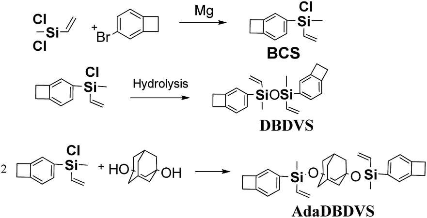 | ||
| Scheme 1 Synthesis of BCB monomers. | ||
Characterization
1H NMR and 13C NMR measurements were carried out using a Bruker DRX-500 spectrometer. Fourier transform infrared (FT-IR) spectra were obtained using a Bruker VERTEX 70 FTIR spectrophotometer at the resolution of 4 cm−1 with 32 scans. Differential scanning calorimetry (DSC) was conducted using a TA Q200 calorimeter. Thermogravimetric analysis (TGA) was performed using a TA Q500 at the heating rate of 10 °C min−1 under a nitrogen flow of 50 mL min−1. Dynamic mechanical analysis (DMA) was carried out using a TA Instruments Q800 in the three-point bending mode at the heating rate of 3 °C min−1 with the test frequency of 1 Hz. The CTE was measured using a TMA Q400 thermomechanical analyzer in the expansion mode at the heating rate of 5 °C min−1. Dielectric property was measured by the parallel-plate capacitor method using a Keysight E4980A precision LCR meter and a Keysight 16451B as the test fixture at room temperature. Atomic force microscopy (AFM) was carried out using a SPM Multimode 8 Bruker.Synthesis of the monomers
![[thin space (1/6-em)]](https://www.rsc.org/images/entities/char_2009.gif) :1) to afford DBDVS (transparent liquid, 86%). 1H-NMR (CDCl3, 500 MHz, δ/ppm): 7.44–7.47 (d, 1H), 7.29 (s, 1H), 7.08–7.11 (d, 1H), 6.25–6.33 (dd, 1H), 6.05–6.11 (dd, 1H), 5.81–5.87 (dd, 1H), 3.22 (CH2–CH2, s, 4H), 0.45 (CH3, s, 3H). 13C NMR (CDCl3, 125 MHz, δ/ppm): 147.6, 145.5, 137.9, 136.0, 133.5, 132.0, 127.4, 121.8, 29.8, −0.70.
:1) to afford DBDVS (transparent liquid, 86%). 1H-NMR (CDCl3, 500 MHz, δ/ppm): 7.44–7.47 (d, 1H), 7.29 (s, 1H), 7.08–7.11 (d, 1H), 6.25–6.33 (dd, 1H), 6.05–6.11 (dd, 1H), 5.81–5.87 (dd, 1H), 3.22 (CH2–CH2, s, 4H), 0.45 (CH3, s, 3H). 13C NMR (CDCl3, 125 MHz, δ/ppm): 147.6, 145.5, 137.9, 136.0, 133.5, 132.0, 127.4, 121.8, 29.8, −0.70.For preparing the polymeric coatings for the AFM test, the monomer (1.0 g) was dissolved in mesitylene (3.0 g) and refluxed for 30 h to afford the oligomers. Then, the oligomer was spin-coated onto the silicon wafer and cured at 250 °C for about 3 h and at 280 °C for 0.5 h under a N2 atmosphere.
Results and discussion
Preparation and characterization of the BCB monomers
The route of BCB monomers synthesis is shown in Scheme 1. First, BCB-functionalized chlorosilane (BCS) was prepared by dichloromethylvinylsilane with 4Br-BCB by Grignard reaction. Then, the prepared BCS was hydrolysed and condensed in the presence of pyridine, as the acid-binding agent, to afford DBDVS. The prepared BCS, which contains a Si–Cl group, can also react with silanols and alcohols such as 1,3-adamantanediol to introduce BCB group, which provides a method for the BCB-functionalization of hydroxyl-containing organic and inorganic surface.Fig. 1 shows the 1H NMR spectra of DBDVS and AdaDBDVS. In DBDVS, the protons (H1) of the methyl group attached to silicon and the methylene protons (H6) of the four-membered ring of the BCB group are observed at 0.45 and 3.22 ppm, respectively. The protons of the vinyl group attached to silicon show three groups of peaks at 5.81–5.87 ppm, 6.05–6.11 ppm, and 6.25–6.33 ppm. The peaks at 7.10, 7.29, and 7.46 ppm are attributed to the protons of the benzene ring of BCB. AdaDBDVS shows a 1H NMR spectrum similar to that of DBDVS, with the difference that the spectrum of AdaDBDVS shows the peaks for the adamantane protons between 1.3 ppm and 2.4 ppm.
 | ||
| Fig. 1 1H NMR spectra of DBDVS and AdaDBDVS. | ||
Fig. 2 shows the 13C NMR spectra of DBDVS and AdaDBDVS, with all carbon atoms in DBDVS and AdaDBDVS clearly assigned. Among these, the peaks at 29.9 and 29.8 ppm are assigned to the methylene carbons of the four-membered ring of BCB group for both DBDVS and AdaDBDVS. The methyl carbons attached to silicon show peaks at −0.7 and −0.25 ppm for DBDVS and AdaDBDVS, respectively. Overall, 1H and 13C NMR spectra of DBDVS and AdaDBDVS demonstrate that all the protons and carbons are consistent with the structure of DBDVS and AdaDBDVS.
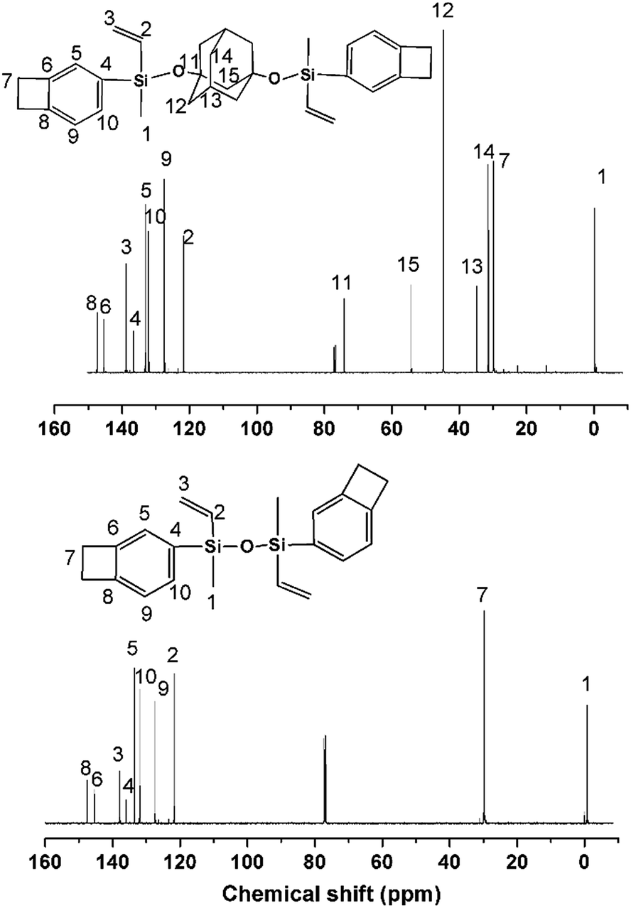 | ||
| Fig. 2 13C NMR spectra of DBDVS and AdaDBDVS. | ||
The FTIR spectra of DBDVS and AdaDBDVS are shown in Fig. 3. For DBDVS, the bands at 2962 cm−1 and 2929 cm−1 are ascribed to the C–H stretching vibration of –CH3. The band at 2828 cm−1 is due to the C–H stretching vibration of methylene in the four-membered ring of BCB. The band at 1593 cm−1 is due to the C![[double bond, length as m-dash]](https://www.rsc.org/images/entities/char_e001.gif) C stretching vibration of the vinyl group.20 Furthermore, the band at 1464 cm−1 is due to the in-plane deformation vibration of the C–H of the methylene in the strained four-membered ring of BCB, and the bands at 1404 cm−1 and 1256 cm−1 are due to the δas(C–H) and δs(C–H) of Si–CH3, respectively. The strong band at 1051 cm−1 is assigned to the Si–O–Si stretching vibration. The absorption band at 789 cm−1 is due to the stretching vibration of Si–C. The bands at 1009 cm−1 and 956 cm−1 are assigned to the bending vibration of C–H in CH2CH. The AdaDBDVS monomer shows an FTIR spectrum similar to that of DBDVS. The difference is the presence of strong bands at 1072 cm−1 and 1051 cm−1, which are assigned to Si–O–C, and some other bands assigned to C–C, CH2 and CH vibrations.
C stretching vibration of the vinyl group.20 Furthermore, the band at 1464 cm−1 is due to the in-plane deformation vibration of the C–H of the methylene in the strained four-membered ring of BCB, and the bands at 1404 cm−1 and 1256 cm−1 are due to the δas(C–H) and δs(C–H) of Si–CH3, respectively. The strong band at 1051 cm−1 is assigned to the Si–O–Si stretching vibration. The absorption band at 789 cm−1 is due to the stretching vibration of Si–C. The bands at 1009 cm−1 and 956 cm−1 are assigned to the bending vibration of C–H in CH2CH. The AdaDBDVS monomer shows an FTIR spectrum similar to that of DBDVS. The difference is the presence of strong bands at 1072 cm−1 and 1051 cm−1, which are assigned to Si–O–C, and some other bands assigned to C–C, CH2 and CH vibrations.
 | ||
| Fig. 3 FTIR spectra of DBDVS and AdaDBDVS monomers. | ||
Curing behaviour of the BCB monomers of DBDVS and AdaDBDVS
The curing behaviour of the DBDVS and AdaDBDVS monomers was studied by DSC at the ramping rate of 10 °C min−1 (Fig. 4). Both monomers display a similar exothermic behaviour, with an onset at 200 °C and a maximum at 258–259 °C, which is similar to that of DVS-BCB. The exothermic enthalpy of polymerization of DBDVS and AdaDBDVS are 698 and 588 J g−1, respectively. Their similar exothermic curing behaviour indicates that the reactivity of the BCB group of DBDVS and AdaDBDVS, with independent vinyl groups on the silicon atoms, is similar to the reactivity of the BCB group, with vinylidene groups linked to BCB in DVS-BCB.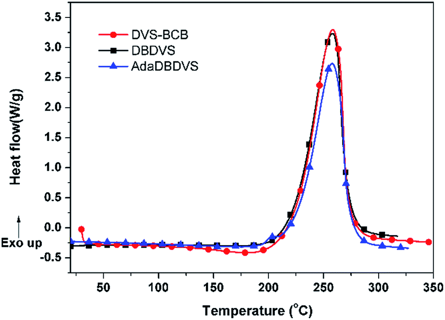 | ||
| Fig. 4 DSC curves of DBDVS and AdaDBDVS. | ||
The FTIR spectra of the cured resins was compared with the FTIR spectra of their corresponding monomers, as it can be seen in Fig. 5. After curing, the bands at 2828 and 1464 cm−1 for BCB and the bands at 1593, 1009, and 956 cm−1 for the vinyl groups completely disappeared, which indicates that the main curing mechanism for the BCB-based monomers is the Diels–Alder cyclization between the reactive o-quinodimethane moieties and alkene groups.19 Moreover, new bands at 3030, 1597, 1557, and 1490 cm−1 of benzene ring appear in the final resins. In summary, these results indicated that the final resins had been completely cured.
 | ||
| Fig. 5 FTIR spectra of the cured resins compared with that of their corresponding monomers. | ||
Properties of the cured resins
TGA was used to evaluate the thermal stability of the cured resins (Fig. 6). The temperatures of 5% weight loss (T5%) of DVS-BCB, DBDVS, and AdaDBDVS are 446, 453, and 449 °C in N2, respectively. Compared to DVS-BCB, the decomposition temperatures of cured DBDVS and AdaDBDVS are slightly higher. This demonstrates that both the cured DBDVS and AdaDBDVS show good thermal stability, which is similar to that of the cured DVS-BCB. | ||
| Fig. 6 TGA curves of cured DVS-BCB, DBDVS and AdaDBDVS. | ||
Fig. 7 shows the DMA curves of the cured BCB resins compared with those of DVS-BCB. The initial storage modulus of cured DVS-BCB is 2.3 GPa at 50 °C. The storage modulus decreases to 0.9 GPa at 250 °C. The damping factor (δ) gradually increases and peaks to 0.09 at about 300 °C. This may be ascribed to the movement of Si–O–Si segment in the cross-linked network. On the other hand, our prepared DBDVS exhibits a higher storage modulus of 2.8 GPa at 50 °C. Even when the temperature reaches 380 °C, the cured DBDVS still exhibits a high storage modulus of 1.6 GPa. Moreover, the damping factor is lower than 0.03 from 50 to 380 °C, and no peak is observed. This indicates that the cured DBDVS shows excellent stiffness within a wide range of temperatures, and no glass transition appears below 380 °C, which is superior to the cured DVS-BCB. Furthermore, the cured AdaDBDVS shows a storage modulus of 2.7 GPa at 50 °C, 1.2 GPa at 300 °C, and 0.5 GPa at 380 °C. The damping factor of AdaDBDVS is lower than that of DVS-BCB but higher than that of DBDVS. Compared with DBDVS, the introduction of a rigid adamantane group in the main chain increases the distance of the cross-linking point, which decreases the cross-linking density and leads to a decreased stiffness.
 | ||
| Fig. 7 DMA curves of cured DVS-BCB, DBDVS, and AdaDBDVS. | ||
To better understand the properties and structures, the cured structures of DVS-BCB and DBDVS were drawn and are shown in Scheme 2. For cured DVS-BCB, every silicon atom is bridged by two chains. However, in the structure of DBDVS, every silicon atom is bridged by three chains. This means that cured DBDVS possesses a higher cross-linking density than DVS-BCB, which makes DBDVS show higher stiffness and a higher glass transition temperature.
 | ||
| Scheme 2 Curing mechanism and simplified chemical structures of cured DBDVS and DVS-BCB (the dipole moment was obtained by GAMESS simulation). | ||
Fig. 8 shows the TMA curves of the cured polymers (left) and the change in the CTE versus temperature (right). The CTE values of the polymers from 30 to 275 °C and above 350 °C are listed in Table 1. From 30 to 275 °C, DBDVS shows the smallest CTE of 47.8 ppm per °C, which is lower than that of DVS-BCB (60.6 ppm per °C). According to the curves of the change of CTE versus temperature (right), both DVS-BCB and DBDVS show low CTE less than 50 ppm per °C below 150 °C. However, the CTE of DVS-BCB swiftly increases above 150 °C and reaches 70–80 ppm per °C. Below 250 °C, DBDVS shows steady and small CTE below 50 ppm per °C. The lower CTE of DBDVS indicates that DBDVS has better thermal mechanical properties and dimensional stability.
 | ||
| Fig. 8 TMA curves of the cured polymers (left) and CTE versus temperature (right). | ||
| Cured resins | E′a (MPa) | Tgb (°C) | T5 wt%c (°C) | CTEd (ppm per °C) | Ke | Df (10−3) | Rag (nm) | |
|---|---|---|---|---|---|---|---|---|
| 50 °C | 300 °C | |||||||
| a Storage modulus.b Glass transition temperature.c 5% weight loss temperature.d Coefficient of thermal expansion between 30 and 275 °C.e Dielectric constant (K) at 1 MHz.f Dielectric loss (D) at 1 MHz.g Average surface roughness in an area of 1.0 × 1.0 μm2. | ||||||||
| DVS-BCB | 2280 | 490 | 293 | 446 | 60.6 | 2.65 | 2.80 | |
| DBDVS | 2845 | 2120 | >380 | 453 | 47.8 | 2.72 | 0.45 | 0.374 |
| AdaDBDVS | 2730 | 1720 | >380 | 449 | 64.2 | 2.78 | 0.81 | 0.364 |
Fig. 9 shows the dielectric property of the bulk polymers. The dielectric constant of all the polymers remained almost unchanged over the frequency range from 100 kHz to 1.2 MHz. The dielectric constant of the cured DBDVS is 2.72 at 1 MHz, which is slightly higher than that of the cured DVS-BCB (2.64 at 1 MHz). According to the Debye equation, the dielectric constant of the materials is mainly dependent on the dipole moment in the polymer materials. To understand the relationship between structure and dielectric properties, a GAMESS simulation analysis of the model structure of the cured resins (shown in Scheme 2) was performed. The result shows that the simplified model structure of cured DVS-BCB has a dipole moment of 0.361 Debye. On the other hand, the dipole moment of the simplified model of the cured DBDVS, in which thbenzene ring is directly attached to a silicon atom, is 0.778 Debye. Along with the silicon atom with four different replacement groups, the dipole moment of cured DBDVS with a lower symmetry, may be higher than that of cured DVS-BCB. Thus, DBDVS shows a larger dielectric constant. Compared with cured DBDVS, cured AdaDBDVS has a similar chemical structure with an additional adamantane–oxygen group in the main chain. According to the test result, the introduction of adamantane in the structure by this method does not lead to a decrease in the dielectric constant.
 | ||
| Fig. 9 Frequency dependency of the dielectric constant and dielectric loss of the polymers at room temperature. | ||
Furthermore, the cured DBDVS shows extremely low dissipation factor of 0.00045 at 1 MHz, which is lower than that of cured DVS-BCB (0.0028 at 1 MHz). This may be due to the fact that the cross-linking density of DBDVS is higher than that of DVS-BCB, which restricts the movement of the electric dipole in Si–O–Si. The cured DBDVS with an extremely low dielectric loss may be an ideal alternative candidate for interlayer dielectric materials.
The surface uniformity and planarity of the polymer coatings on a silicon wafer was investigated by AFM. Both planar graphs and stereograms are shown in Fig. 10. Measurement results show that the average surface roughness Ra of the cured DBDVS and AdaDBDVS is 0.374 nm and 0.364 nm in a 1.0 × 1.0 μm2 area, respectively. The excellent uniformity and planarity of the polymeric coatings is desirable for the processing of low-K interlayers.
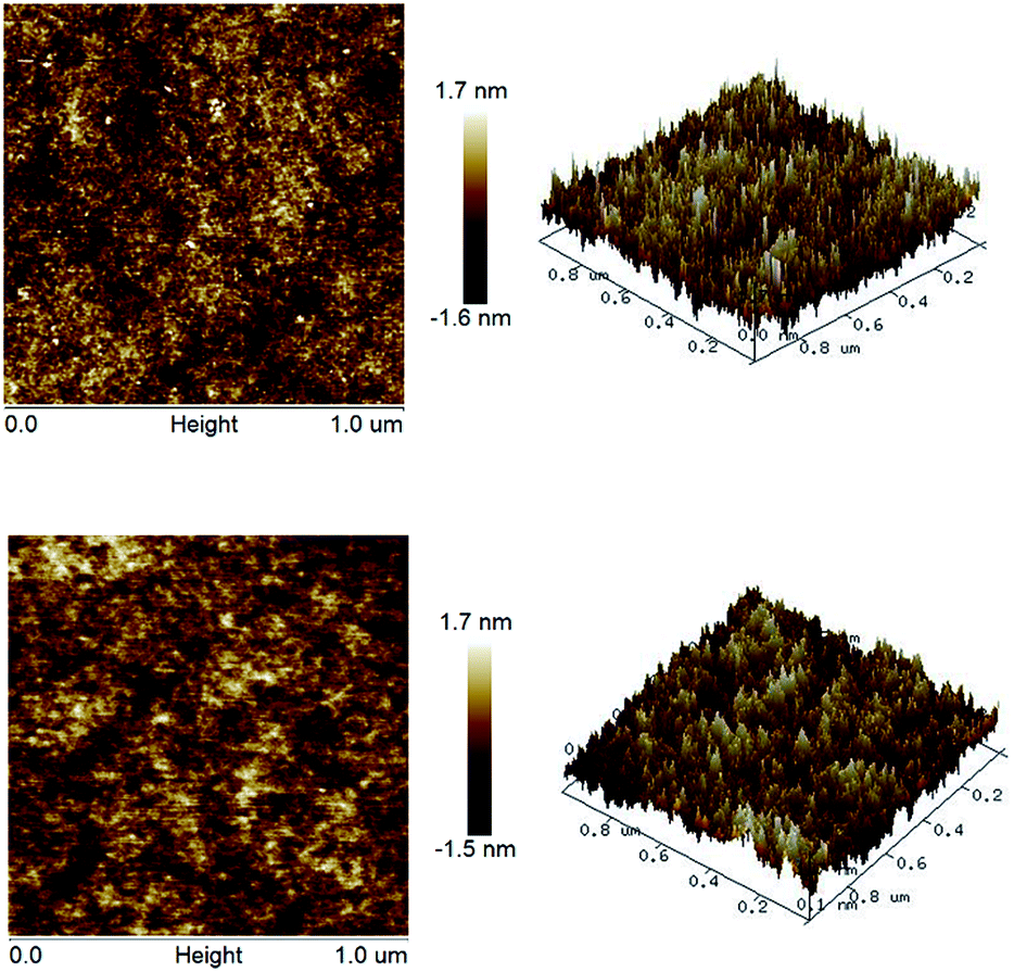 | ||
| Fig. 10 AFM images of polymeric coatings on a silicon wafer: p-DBDVS (up) and p-AdaDBDVS (bottom); (left) planar graph, (right) stereogram. | ||
Conclusions
Herein, BCB resins of DBDVS and AdaDBDVS were successfully synthesized by the hydrolysis and condensation of BCB-functionalized chlorosilane (BCS). The cured DBDVS and AdaDBDVS show slightly improved thermal stability over DVS-BCB. The cross-linking density of DBDVS and AdaDBDVS is higher than that of DVS-BCB. Therefore, the cured DBDVS and AdaDBDVS exhibit better thermal mechanical and electrical properties such as a higher storage modulus, a higher glass transition temperature, and a lower dielectric loss (dissipation factor). Especially, the cured DBDVS can maintain a high storage modulus within a wide temperature range from room temperature to 300 °C. Additionally, the cured DBDVS shows a low CTE of 47.8 ppm per °C from 30 to 275 °C as well as an extremely low dissipation factor of 0.00045 at 1 MHz. Moreover, our method of introducing a BCB group by the reaction of BCB-functionalized chlorosilane with alcohols or silanols may provide an alternative strategy for the synthesis of BCB resin. In addition, the BCB-functionalized chlorosilane can also be used as a silane coupling agent for the treatment of inorganic and organic particles with hydroxyl-containing surface to prepare composites.Acknowledgements
This research was sponsored by the National Natural Science Foundation of China (NSFC No. 51403039), the Natural Science Foundation of Shanghai (13ZR1451300), and the Fudan's Undergraduate Research Opportunities Program (FDUROP No. 16439).References
- T. Homma, Mater. Sci. Eng., 1998, 23, 243 Search PubMed.
- G. Maier, Prog. Polym. Sci., 2001, 26, 3 CrossRef CAS.
- W. Volksen, R. D. Miller and G. Dubois, Chem. Rev., 2010, 110, 56 CrossRef CAS PubMed.
- S. Chang, S. Jang, S. Lin and M. Liang, Thin Solid Films, 2004, 466, 54 CrossRef CAS.
- F. Lv, L. Liu, Y. Zhang and P. Li, J. Appl. Polym. Sci., 2015, 132, 41480 Search PubMed.
- S. Eslava, L. Zhang, S. Esconjauregui, J. Yang, K. Vanstreels, M. R. Baklanov and E. Saiz, Chem. Mater., 2013, 25, 27 CrossRef CAS.
- M. Usman, S. Mendiratta and K. Lu, ChemElectroChem, 2015, 2, 786 CrossRef CAS.
- X. Zhao and H. Liu, Polym. Int., 2010, 59, 597 CAS.
- A. S. Parveen, P. Thirukumaran and M. Sarojadevi, Polym. Adv. Technol., 2014, 25, 1538 CrossRef CAS.
- M. Jia, Y. Li, C. He and X. Huang, ACS Appl. Mater. Interfaces, 2016, 8, 26352 CAS.
- J. H. Yim, Y. Y. Lyu, H. D. Jeong, S. K. Mah, J. Hyeon-Lee, J. H. Hahn, G. S. Kim, S. Chang and J. G. Park, J. Appl. Polym. Sci., 2003, 90, 626 CrossRef CAS.
- H. S. Lee, S. Choi, K. Baek, E. C. Lee, S. M. Hong, J. Lee and S. S. Hwang, Macromol. Res., 2012, 20, 1131 CrossRef CAS.
- X. Zuo, J. Chen, X. Zhao, S. Yang and L. Fan, J. Polym. Sci., Part A: Polym. Chem., 2008, 46, 7868 CrossRef CAS.
- X. Zuo, R. Yu, S. Shi, Z. Feng, Z. Li, S. Yang and L. Fan, J. Polym. Sci., Part A: Polym. Chem., 2009, 47, 6246 CrossRef CAS.
- L. Kong, Y. Cheng, Y. Jin, Z. Ren, Y. Li and F. Xiao, J. Mater. Chem. C, 2015, 3, 3364 RSC.
- J. Wang, Y. Luo, K. Jin, C. Yuan, J. Sun, F. He and Q. Fang, Polym. Chem., 2015, 6, 5984 RSC.
- A. K. Schrock, Utility patent, US4812588, 1989.
- J. Tong, S. Diao, K. Jin, C. Yuan, J. Wang, J. Sun and Q. Fang, Polymer, 2014, 55, 3628 CrossRef CAS.
- J. Yang, Y. Cheng and F. Xiao, Eur. Polym. J., 2012, 48, 751 CrossRef CAS.
- J. E. Drake, A. Vahradian and B. M. Glavincevski, Can. J. Chem., 1983, 61, 2712 CrossRef CAS.
| This journal is © The Royal Society of Chemistry 2017 |