DOI:
10.1039/C7RA00058H
(Paper)
RSC Adv., 2017,
7, 26130-26135
Point-defect-induced colossal dielectric behavior in GaAs single crystals
Received
3rd January 2017
, Accepted 1st May 2017
First published on 16th May 2017
Abstract
We herein reported colossal dielectric constant (CDC) behavior in GaAs single crystals. This behavior appears in the temperature range above room temperature and results from the bulk effect due to polaron relaxation caused by hopping motion of EL2 defects. When temperature rises higher than 420 K, the interfacial contribution due to Maxwell–Wagner relaxation caused by sample/electrode contacts appears. When temperature is higher than 560 K, the CDC behavior is mainly contributed by the interfacial effect. These features are quite different from the CDC behavior found in oxides, and therefore, the CDC behavior in GaAs single crystals is considered as a new type of the CDC family. Our results underscore the role of point-defects in CDC behavior and suggest that defect engineering can be a promising strategy to achieve superior CDC behavior in both oxide and non-oxide materials.
1. Introduction
The continual tendency toward device miniaturization and increasing perceived demand for high-density energy storage have triggered a burst of research activities in searching for colossal permittivity materials.1,2 Permittivity over 104, is now termed as colossal dielectric constant (CDC).3,4 The current existing CDC materials can be classified into two types: (1) ferroelectric materials as represented by Ba/Pb-based perovskite oxides characterized by a sharp permittivity at the temperature of ferroelectric phase transition,5 and (2) non-ferroelectric materials varying from single to multicomponent oxides characterized by a colossal and flat dielectric constant over a wide temperature range around room temperature.6–9 Nevertheless, the former suffers from the toxicity and strong temperature dependence of the permittivity; the latter shows the weakness of relatively high dielectric loss. These formidable problems strongly limit the practical application of both types of materials. Therefore, much work is warranted on the searching for new CDC materials suitable for real device application.
Since CDC behavior in non-ferroelectrics and relaxors is contributed exclusively by defect dipolar and/or space charge polarizations, the empirical methods to explore new CDC materials are (1) introducing defect dipoles through doping1,10,11 and (2) engineering the space charge polarization by fabricating various artificial interfaces such as core–shell12 and hybrid nanolaminate structures.13 It is worth emphasizing that all the efforts were performed in oxides. In contract, CDC behavior in non-oxide materials remains conspicuously absent. It raises the question: is CDC behavior peculiar to oxides?14 Or in other word, does the CDC behavior appear in non-oxide materials?
In fact, point defects and artificial interfaces were widely engineered to tune the properties of non-oxides.15,16 It is, therefore, expected that non-oxides could be yet another promising CDC materials. Excited by this expectation, we performed dielectric investigations on GaAs crystals. The sample is used because it has recently gained a revived interest as replacement to silicon in future metal-oxide-semiconductor field-effect transistors.17,18 Point defects, such as oxygen, AsGa antisite, Ga/As vacancies, and the complex of these defects, are known to play an important role in determining the properties of GaAs.19–22 Our results show that GaAs crystals exhibit CDC behavior in the temperature above room temperature. This behavior is argued to be a bulk effect caused by defect points.
2. Experimental
The (001) oriented GaAs single crystals were purchased from Hefei Kejing Materials Technology Co., Ltd. Dielectric properties in both temperature and frequency domains were measured using a Wayne Kerr 6500B precise impedance analyzer (Wayne Kerr Electronic Instrument Co., Shenzhen, China) with the sample mounted in a holder placed inside a PST-2000HL dielectric measuring system (Partulab Co., Wuhan, China). The temperature domain dielectric properties were measured at fixed frequencies by varying temperature with a heating ramp of 2 K min−1. The frequency domain dielectric properties were measured at fixed temperatures by scanning frequency from 102 to 106 Hz. The ac measuring signal was 100 mV rms. Electrodes were made by printing silver paste on both sides of the samples and then fired at 1073 K for 2 h in air in order to remove the polymeric component and get good contact. To get detailed information about the dielectric properties of GaAs single crystals, the dielectric data were analyzed in terms of three dielectric functions: dielectric permittivity ε*, electric modulus M*, and impedance Z*. Electron spin resonance (ESR) measurement was carried out using a Bruker EMX-plus model spectrometer operating at X-band frequency (υ ≅ 9.4 GHz).
3. Result and discussion
Fig. 1(a) and (b) shows, respectively, the temperature (T) dependence of the dielectric constant (ε′) and loss tangent (tan![[thin space (1/6-em)]](https://www.rsc.org/images/entities/char_2009.gif) δ) for a GaAs crystal measured under different frequencies (f). It is seen that a stepwise increase in ε′(T) leads to a colossal and weak temperature-dependent dielectric constant over 4k around 400 K of the crystal. The stepwise increase is accompanied by a thermally activated relaxation peak in tanδ characterizing the typical the CDC behavior as reported in oxides.2,8 However, compared with the CDC behavior in oxides, there are two main features worth to be emphasized: (1) the temperature of the stepwise increase in ε′ for the present sample, e.g., 350 K for the curve recorded at 1 kHz, is much higher than those reported in oxides. For example, the stepwise increase temperature recorded with the same frequency of 1 kHz were found to be around 100, 150, 175, and 200 K for CaCu3Ti4O12,23 TbMnO3,8 LaFeO3,24 and La2CuTiO6,25 respectively. (2) The stepwise increase in oxides is almost invisible in the curves measured with frequencies higher than 1 MHz. Whereas the present sample still shows a stepwise increase larger than 4k for the curve measured under 3 MHz. These features indicate that the CDC behavior in GaAs is different from that in oxides.
δ) for a GaAs crystal measured under different frequencies (f). It is seen that a stepwise increase in ε′(T) leads to a colossal and weak temperature-dependent dielectric constant over 4k around 400 K of the crystal. The stepwise increase is accompanied by a thermally activated relaxation peak in tanδ characterizing the typical the CDC behavior as reported in oxides.2,8 However, compared with the CDC behavior in oxides, there are two main features worth to be emphasized: (1) the temperature of the stepwise increase in ε′ for the present sample, e.g., 350 K for the curve recorded at 1 kHz, is much higher than those reported in oxides. For example, the stepwise increase temperature recorded with the same frequency of 1 kHz were found to be around 100, 150, 175, and 200 K for CaCu3Ti4O12,23 TbMnO3,8 LaFeO3,24 and La2CuTiO6,25 respectively. (2) The stepwise increase in oxides is almost invisible in the curves measured with frequencies higher than 1 MHz. Whereas the present sample still shows a stepwise increase larger than 4k for the curve measured under 3 MHz. These features indicate that the CDC behavior in GaAs is different from that in oxides.
 |
| | Fig. 1 Temperature dependence of the dielectric constant (a) and loss tangent (b) for a GaAs single crystal measured under different frequencies. | |
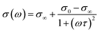
To decipher the nature of the CDC behavior in GaAs, knowledge of the mechanism of the observed relaxation is of paramount importance. In doing so, one needs to calculate the relaxation parameters. Nevertheless, a careful examination reveals that the relaxation peak, especially for those measured with high frequency, e.g., 3 MHz, is composed of two close peaks. Meanwhile, an exponentially increasing background in loss tangent at higher temperatures is observed. This background shifts to high temperature and decreases in magnitude with increasing measurement frequency indicating that it is associated with the conductivity [tanδ ∼ σ/ω ∼ exp(−Econd/kBT)/ω, where Econd is activation energy of conductivity, ω = 2πf is angular frequency, and kB is Boltzmann constant]. Both facts strongly limit us in obtaining the relaxation parameters. In this case, the dielectric function of electric modulus M*, defined as M* = M′ + jM′′ = 1/ε* (j is the square root of −1), is applied. It shares the same mechanism of the dielectric permittivity (ε*) and considered to be a powerful function in revealing the relaxation shadowed by background.26
Fig. 2(a) shows the spectroscopic plots of the imaginary part of the electric modulus for a GaAs crystal recorded at a series of temperatures. Owing to the absence of background, two distinct relaxation peaks can be clearly seen. For brevity, these relaxations are named as R1 and R2 in the order of ascending temperature. The peak position, fP, is plotted as a function of the reciprocal of the measuring temperature (1000/T) in terms of the Arrhenius law
| | |
fP = f0exp(−Ea/kBT)
| (1) |
where
f0 is pre-exponential factor and
Ea is activation energy of the relaxation.
Fig. 2(b) displays Arrhenius plots of the observed relaxations. It is seen that both relaxations follow perfect Arrhenius relation. The activation energy is calculated to be 0.80 and 0.48 eV for R1 and R2, respectively. The activation energy of R1 agrees perfectly with that of the EL2 defects (0.80 eV).
22 EL2 defects in GaAs has been generally accepted to be associated with As antisite (As
Ga) point defects,
27,28 which are known to be double donors. The singly charged state As
Ga+ has unpaired sp electrons and hence can be detected by ESR spectrum. The ESR result recorded at room temperature is shown in the inset of
Fig. 2(b), which shows a resonant line resulting from the As
Ga+.
29 This result confirms the existence of the As antisite point defects. On the other hand, the charged defects in the crystal appear to be polarons, because they will be frozen at low enough temperatures by their surrounding medium
via repelling (attracting) the like (opposite) ions. At high enough temperatures, these defects will be thermally activated and hop randomly to nearby positions leading to dipolar effect.
30 Under an applied field, the polarons are electrically activated and hop with respect to the applied field yielding re-orientation polaron relaxation.
31 Therefore, the relaxation R1 is point-defect related. For a polaron relaxation, the loss tangent and electric modulus attain their maxima of (tan
δ)
max and (
M′′)
max at the frequency
ftanδ and
fM, respectively. Based on these parameters, two Arrhenius-like plots are predicated
32,33| |
 | (2) |
| |
 | (3) |
where
WH and
Eg are related to polaron hopping and formation energy, respectively.
Eqn (2) and (3) predicate a fingerprint nature for a polaron relaxation, namely two Arrhenius-like lines in the plots of log((
ftanδ)
2/
fM) and log(
T(tan
δ)
max2/(
M′′)
max) against 1/
T. To corroborate the polaronic nature of R1, the spectroscopic plots of the loss tangent at a series of temperatures are displayed in
Fig. 3, from which the maxima of (tan
δ)
max as well as the position
ftanδ can be deduced. Together with the spectroscopic plots of electric modulus shown in
Fig. 2(a), the two Arrhenius-like relationships are clearly evidenced as shown in the inset of
Fig. 3. Linear fittings, shown as solid lines in the inset, yield
WH = 0.750 eV and
Eg/2 = 0.052 eV. In the case of small polaron hopping process, the activation energy for the conduction follows
Econ =
WH +
Eg/2.
33,34 The sum of
WH and
Eg/2 equals 0.802 eV, which agrees perfectly with the activation energy of R1. Since the hopping process of small polaron not only yields bulk conduction but also gives rise to dielectric relaxation, both aspects are strongly related and thus show close value of activation energy. This result firmly confirms the polaronic nature of the R1.
 |
| | Fig. 2 (a) Frequency dependence of electric modulus for GaAs crystal measures at various temperatures. (b) Arrhenius plots of the relaxations observed in (a). The solid lines are linear fitting results. Inset: ESR spectrum of GaAs crystal recorded at room temperature. | |
 |
| | Fig. 3 Frequency dependence of loss tangent of GaAs crystal measures at various temperatures. The inset shows the Arrhenius relations (ftanδ)2/fM and T(tanδ)max2/M′′max versus 1000/T. The solid lines are linear fitting results. | |
To clarify the nature of R2, we performed impedance analysis under different dc biases at temperatures where R2 is the predominant relaxation of GaAs. A typical result recorded at 450 K is present in Fig. 4. This temperature is chosen, because at this temperature only R2 can be seen and R1 moves to a higher frequency out of the measuring frequency window [see Fig. 2(a)]. It is clearly seen that the complex impedance plot behaves as a semicircle indicative of R2. The inset shows an enlarged view of the impedance plot in the high frequency range. It shows that a high-frequency tail independent of dc bias indicative of R1 is almost invisible. We would like to stress that the semicircle can be notably depressed by the dc bias. This finding demonstrates that R2 is an interfacial relaxation or Maxwell–Wagner relaxation, because a Maxwell–Wagner relaxation is associated with a Schottky barrier, whose intensity as well as the Maxwell–Wagner relaxation can be effectively depressed by a dc bias.35 The absence of grain boundaries in the present crystal leads to the conclusion that R2 is a Maxwell–Wagner relaxation associated with the interfaces of sample/electrode contacts.
 |
| | Fig. 4 Complex impedance plots of GaAs crystal recorded at 450 K under different dc biases. The inset show is an enlarged view of the plots in the high-frequency range. | |
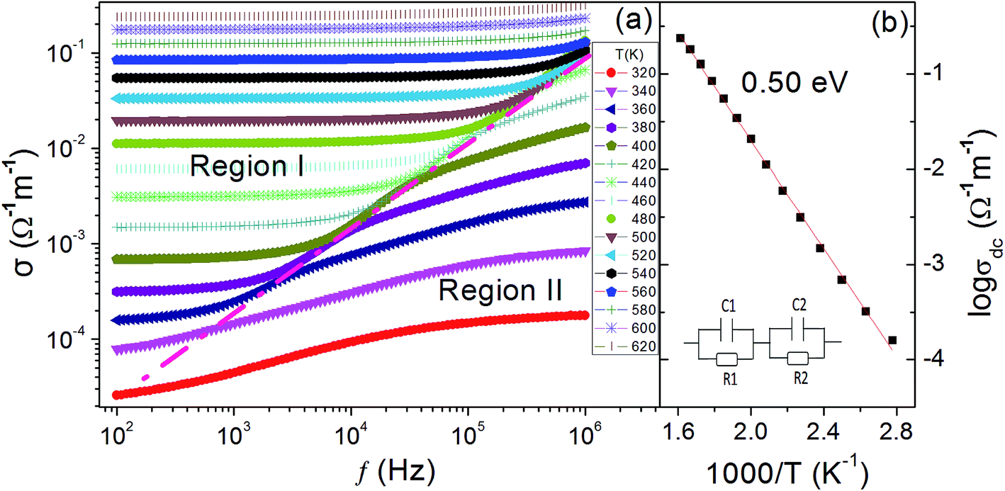
To further convince this point, we conduct ac conductivity analysis. Fig. 5(a) shows the ac conductivity as a function of frequency recorded at different temperatures. The noteworthy observation is that the curves can be clarified into two regions (I and II). In region I, the curves behave as plateaus in the low-frequency range followed by linear increases (in log–log scale) in the high-frequency range. This behavior seems to be the typical feature of the well-known universal dielectric response (UDR) as described by36
| | |
σ(T,f) = σdc + B(T)fs
| (4) |
where
σdc is dc conductivity,
B(
T) and
s are temperature-dependent constants. However, a careful examination reveals that the linear increase is actually a sigmoidal curve which collects the low-frequency
σdc and a high-frequency plateau. The high-frequency plateau is more notable in the curves measured at low temperatures,
e.g., 320 K. This fact indicates that the UDR model fails to describe the ac conductivity. Since both the Maxwell–Wagner and polaron relaxations have contributions to the ac conductivity, in this case, the sample can be modeled by two serially connected
RC (
R = resistor and
C = capacitor) units as shown by the inset in
Fig. 5(b) where the subindex 1 and 2 refer to the bulk and interfacial effects, respectively. Based on the equivalent circuit, the resistance of the system can be written as
37| |
 | (5) |
where
ω = 2π
f is the angular frequency. By considering the behavior at zero and infinite frequencies and introducing the parameters of
A = area of the capacitor and
l = sample thickness,
eqn (5) can be rewritten as
| |
 | (6) |
with
,

, and

 |
| | Fig. 5 (a) Frequency dependence of ac conductivity of GaAs crystal measured at various temperatures. (b) Arrhenius plot of the dc conductivity deduced from (a). The solid line is linear fitting result and the inset is the equivalent circuit. | |
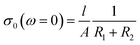
Similar to Debye relaxation, eqn (6) clearly indicates that the ac conductivity shows a low- and high-frequency plateaus with a sigmoidal curve linking them. It is generally accepted that R2 ≫ R1, C2 ≫ C1.38 As a result, σ0 ∼ l/AR2 and σ∞ ∼ l/AR1. This means that the low- and high-frequency plateaus represent the interfacial and bulk contributions, respectively. It, therefore, follows that the region I in Fig. 5(a) represents the interfacial effect. The Arrhenius plot of the dc conductivity deduced from region I of Fig. 5(a) is plotted in Fig. 5(b). The activation energy is calculated to be 0.51 eV, which is comparable with that R2. This finding confirms that the R2 is caused by interfacial effect.
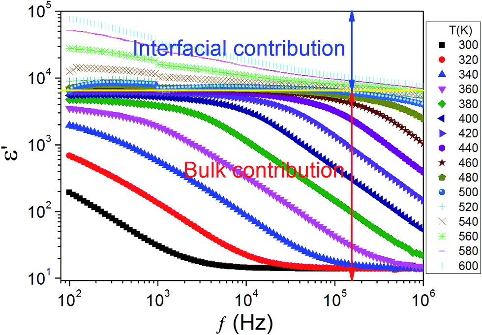
The above results evidence that R1 and R2 are related to bulk and interfacial effects due to polaron and Maxwell–Wagner relaxations, respectively. In order to find out which one dominates the CDC behavior of the GaAs crystal, the frequency dependence of the real part of the complex permittivity was measured at temperatures varying from 300 to 600 K with an increment step of 20 K. As shown in Fig. 6, the CDC behavior of GaAs results from two thermally activated relaxations. The relaxation R1 characterized by a low-frequency plateau and a stepwise decrease in ε′(f) dominates the CDC behavior in the temperature range of T ≤ 540 K. When T ≥ 420 K, though the data points at the lowest frequencies deviate from the low-frequency plateau indicative of the appearance of R2, only when T ≥ 560 K, the contribution to the CDC behavior from R2 outmatches that from R1 (please note the logarithmic scale of the dielectric constant). Therefore, the observed CDC behavior in GaAs crystal is dominated by the bulk effect due to polaron relaxation caused by the hopping motion of EL2 defects in the temperature range below 560 K. While in the temperature range above 560 K, the CDC behavior is mainly contributed by the interfacial effect due to Maxwell–Wagner relaxation caused by the sample/electrode contacts. This behavior is quite different from that observed in CaCu3Ti4O12. The interfacial effect therein contributes ∼3/4 CDC behavior of CaCu3Ti4O12.39 Therefore, the CDC behavior in GaAs crystals can be considered as new type one.
 |
| | Fig. 6 Frequency dependence of the dielectric constant for GaAs crystal measured at various temperatures. | |
4. Conclusions
In conclusion, dielectric properties of GaAs crystals were investigated in the temperature from room temperature to 650 K and frequency range of 102 to 3 × 10⁶ Hz. The crystal shows CDC behavior contributed by bulk and interfacial effects in the temperature ranges below and above 560 K, respectively. The bulk contribution comes from the polaron relaxation caused by the hopping motion of EL2 defects. Whereas the interfacial contribution results form the Maxwell–Wagner relaxation caused by the sample/electrode contacts. The CDC behavior in GaAs crystals is argued to be a new one different form the conventional type reported in oxides.
Acknowledgements
The authors thank financial support from National Natural Science Foundation of China (Grant No. 51572001, 11404002 and 11404003). This work was supported in part by the Weak Signal-Detecting Materials and Devices Integration of Anhui University (Grant No. Y01008411).
References
- W. B. Hu, Y. Liu, R. L. Withers, T. J. Frankcombe, L. Noren, A. Snashall, M. Kitchin, P. Smith, B. Gong, H. Chen, J. Schiemer, F. Brink and J. Wong-Leung, Nat. Mater., 2013, 12, 821–826 CrossRef CAS PubMed.
- C. C. Homes, T. Vogt, S. M. Shapiro, S. Wakimoto and A. P. Ramirez, Science, 2001, 293, 673–676 CrossRef CAS PubMed.
- P. Lunkenheimer, V. Bobnar, A. V. Pronin, A. I. Ritus, A. A. Volkov and A. Loidl, Phys. Rev. B: Condens. Matter Mater. Phys., 2002, 66, 052105 CrossRef.
- P. Lunkenheimer, R. Fichtl, S. G. Ebbinghaus and A. Loidl, Phys. Rev. B: Condens. Matter Mater. Phys., 2004, 70, 172102 CrossRef.
- L. E. Cross, Ferroelectrics, 1987, 76, 241–267 CrossRef CAS.
- P. H. Salame, O. Prakash and A. R. Kulkarni, Ceram. Int., 2016, 42, 13207–13214 CrossRef CAS.
- W. Q. Cao, L. F. Xu, M. M. Ismail and L. L. Huang, Mater. Sci., 2016, 34, 322–329 CAS.
- C. C. Wang, Y. M. Cui and L. W. Zhang, Appl. Phys. Lett., 2007, 90, 012904 CrossRef.
- D. Berardan, S. Franger, D. Dragoe, A. K. Meena and N. Dragoe, Phys. Status Solidi RRL, 2016, 10, 328–333 CrossRef CAS.
- J. B. Wu, C. W. Nan, Y. H. Lin and Y. Deng, Phys. Rev. Lett., 2002, 89, 217601 CrossRef PubMed.
- X. Liu, H. Q. Fan, J. Shi and Q. Li, Sci. Rep., 2015, 5, 12699–12709 CrossRef CAS PubMed.
- X. Y. Zhang, Y. J. Chen, Z. Y. Li and V. G. Harris, J. Alloys Compd., 2017, 692, 950–954 CrossRef CAS.
- W. Li, O. Auciello, R. N. Premnath and B. Kabius, Appl. Phys. Lett., 2010, 96, 162907 CrossRef.
- N. Izyumskaya, Y. Alivov and H. Morkoc, Crit. Rev. Solid State Mater. Sci., 2009, 34, 89–179 CrossRef CAS.
- M. G. Kibria, F. A. Chowdhury, S. Zhao, M. L. Trudeau, H. Guo and Z. Mi, Appl. Phys. Lett., 2015, 106, 113105 CrossRef.
- Z. C. Zhang, B. Xu and X. Wang, Chem. Soc. Rev., 2014, 43, 7870–7886 RSC.
- J. A. Del Alamo, Nature, 2011, 479, 317–323 CrossRef CAS PubMed.
- J. Nah, H. Fang, C. Wang, K. Takei, M. H. Lee, E. Plis, S. Krishna and A. Javey, Nano Lett., 2012, 12, 3592–3594 CrossRef CAS PubMed.
- D. Colleoni and A. Pasquarello, Phys. Rev. B, 2016, 93, 125208 CrossRef.
- H. B. Shu, X. D. Yang, P. Liang, D. Cao and X. S. Chen, J. Phys. Chem. C, 2016, 120, 22088–22095 CAS.
- V. Saltas, A. Chroneos and F. Vallianatos, RSC Adv., 2016, 6, 53324–53330 RSC.
- S. T. Neild, M. Skowronski and J. Lagowski, Appl. Phys. Lett., 1991, 58, 859–861 CrossRef CAS.
- C. C. Wang and L. W. Zhang, Appl. Phys. Lett., 2007, 90, 142905 CrossRef.
- C. Chen, K. B. Xu, Y. M. Cui and C. C. Wang, Mater. Lett., 2012, 89, 153–155 CrossRef CAS.
- W. Z. Yang, M. M. Mao, X. Q. Liu and X. M. Chen, J. Appl. Phys., 2010, 107, 124102 CrossRef.
- C. C. Wang, J. Wang, X. H. Sun, L. N. Liu, J. Zhang, J. Zheng and C. Cheng, Solid State Commun., 2014, 179, 29–33 CrossRef CAS.
- X. F. Zhong, D. S. Jiang, W. Ge and C. Song, Appl. Phys. Lett., 1988, 52, 628–630 CrossRef CAS.
- S. M. Tunhuma, F. D. Auret, M. J. Legodi and M. Diale, J. Appl. Phys., 2016, 119, 145705 CrossRef.
- D. W. Jung, J. P. Noh and N. Otsuka, Phys. B, 2010, 405, 4133–4138 CrossRef CAS.
- C. C. Wang and L. W. Zhang, Appl. Phys. Lett., 2008, 92, 132903 CrossRef.
- A. K. Jonscher, Nature, 1975, 253, 717–719 CrossRef CAS.
- G. J. Wang, C. C. Wang, S. G. Huang, C. M. Lei, X. H. Sun, T. Li and L. N. Liu, J. Am. Ceram. Soc., 2013, 96, 2203–2210 CrossRef CAS.
- E. Iguchi, K. Ueda and W. H. Jung, Phys. Rev. B: Condens. Matter Mater. Phys., 1996, 54, 17431–17437 CrossRef CAS.
- W. H. Jung, J. Mater. Sci. Lett., 2002, 21, 573–575 CrossRef CAS.
- C. C. Wang, M. He, F. Yang, J. Wen, G. Z. Liu and H. B. Lu, Appl. Phys. Lett., 2007, 90, 192904 CrossRef.
- A. K. Jonscher, Nature, 1997, 267, 673–679 CrossRef.
- R. Stumpe, D. Wagner and D. Bauerle, Phys. Status Solidi A, 1983, 75, 143–154 CrossRef CAS.
- P. Lunkenheimer, S. Krohns, S. Riegg, S. G. Ebbinghaus, A. Reller and A. Loidl, Eur. Phys. J.: Spec. Top., 2010, 180, 61–89 CrossRef.
- C. C. Wang, W. Ni, D. Zhang, X. Sun, J. Wang, H. B. Li and N. Zhang, J. Electroceram., 2016, 36, 46–57 CrossRef CAS.
|
| This journal is © The Royal Society of Chemistry 2017 |
Click here to see how this site uses Cookies. View our privacy policy here. 
 Open Access Article
 This Open Access Article is licensed under a
  a,
N. Zhanga,
H. Wanga,
Y. D. Lia,
S. G. Huanga,
Q. J. Li*a,
Y. Yua,
Y. M. Guoa,
X. L. Liu
a,
N. Zhanga,
H. Wanga,
Y. D. Lia,
S. G. Huanga,
Q. J. Li*a,
Y. Yua,
Y. M. Guoa,
X. L. Liu


 ,
,  , and
, and