
 Open Access Article
 This Open Access Article is licensed under a
 Creative Commons Attribution 3.0 Unported Licence
2D free-standing Ge-doped ZnO: excellent electron-emitter and excitation-power-dependent photoluminescence redshift
Yong Sun and
Chengxin Wang *
*
The Key Laboratory of Low-Carbon Chemistry & Energy Conservation of Guangdong Province, State Key Laboratory of Optoelectronic Materials and Technologies, School of Materials Science and Engineering, Sun Yat-sen (Zhongshan) University, Guangzhou 510275, People's Republic of China. E-mail: wchengx@mail.sysu.edu.cn; Fax: +86-20-84113901; Tel: +86-20-84113901
First published on 15th February 2017
Abstract
Two-dimensional (2D) free-standing Ge-doped ZnO nanostructures were synthesized on graphite substrate. A single nanosheet composed of amounts of nanograins with size of ∼20 nm exhibits excellent field electron emission capability that can deliver a current as large as 30 mA cm−2 at E = 9.0 V μm−1. The amazing performance originates from the high electron conductivity owing to Ge doping, as well as the enriched emitting spots on the surface of the structure. Additionally, we observed the temperature- and excited-power-dependent redshift of photoluminescence (PL) in the temperature range of 77–300 K, which was attributed to the local thermal effect driven nonradioactive enhancement. The rich defect and impurity levels result in alternative recombination mechanisms in the temperature range.
Introduction
The imperious demands for various optoelectric functionalities in modern technologies ranging from LED and FED to biosensing have been promoting fundamental research about semiconductors with promising properties,1–3 aiming to achieve advanced device applications. As an important type of third-generation semiconductor, ZnO was confirmed to integrate critical features like a wide direct bandgap (3.37 eV), large exciton binding energy (60 meV), and defect-, temperature- and size-dependent light emission.4–6 Its rich properties have been explored and investigated as a novel device. For example, Wang's group carried out some advanced work about the energy conversion by utilizing the piezoelectricity and thermoelectricity of wurtzite ZnO, which presents a promising nanogenerator application of nanostructure ZnO.7,8 Yang et al. proved experimentally that 1D ZnO nanostructures could be used in future photonic devices both for light transport and as micro-nano laser resources.9,10There are extremely rich levels in doped ZnO, which can be introduced by various defects and impurities. Recently, the topic of light emission resulting from NBE (Near-band Edge Emission) and defects has been frequently investigated. Many interesting light emission behaviors dominated by various physical mechanisms have been exposed. Generally speaking, the emission related to the UV region, often observed in highly crystalline ZnO, is mainly attributed to NBE-like recombination of defect-bound excitons and free excitons owing to the very large exciton binding energy (60 meV). The highly efficient UV light emission makes ZnO a good candidate to be applied in photonic and optoelectronic devices operated in the UV region. On the other hand, defects are often introduced into the lattice to modify the electric structure, which can result in rich optical phenomenon, i.e. tunable emission driven by excited wavelength, excited power, and even temperature.11–13 Actually, the renormalized level would absolutely influence the performance of the material in other fields, such as electrical properties.14 Therefore, the doping design of ZnO nanostructures also provides an important way to endow them with advanced properties and improved performance for device application. Using Ge as the dopant, ZnO with improved photonic and electronic properties has been prepared. Various synthesis methods have been developed, such as pulsed laser deposition technique,15 colloidal synthesis16 and radio-frequency magnetron sputtering.17 Ge-doped ZnO crystals have been proved to exhibit enhanced visible-light transmittance,15 interesting plasmonic behavior,16 and improved bias stability in FET applications17 and so on.
In this work, we realized 2D Ge doped ZnO nanostructures with the common chemical vapor deposition method (CVD). The field electrons emission performance and the PL properties were investigated. Some interesting topics were proposed during the test, such as the large current emission and power-dependent redshift of the PL spectrum. We hope these results can enrich the ZnO research in future.
Experimental
The sample synthesis was carried out in a self-designed and -built furnace as demonstrated previously.18–20 In detail, a mixture of ZnO and C black (30 mg, atomic ratio 2![[thin space (1/6-em)]](https://www.rsc.org/images/entities/char_2009.gif) :1) was put at the center of a polished ceramic sheet and 5 mg of GeO2 was placed by the side. A piece of graphite sheet was placed 6 cm away from the GeO2 powder. The whole ceramic sheet was then pushed into a semi-closed corundum tube, which was pushed into the furnace with ZnO/C powder in the high temperature zone. After the chamber vacuum degree reached ∼10−1 Pa by using a mechanic pump, H2 at a flow of 100 sccm and CH4 at a flow of 5 sccm were introduced until the pressure of the chamber was 5 kPa. At the same time, the temperature was raised to 1150 °C by changing the heating power. Both the pressure and temperature were held for 60 min. Finally, the brown sample was found to have grown steadily on the graphite surface.
:1) was put at the center of a polished ceramic sheet and 5 mg of GeO2 was placed by the side. A piece of graphite sheet was placed 6 cm away from the GeO2 powder. The whole ceramic sheet was then pushed into a semi-closed corundum tube, which was pushed into the furnace with ZnO/C powder in the high temperature zone. After the chamber vacuum degree reached ∼10−1 Pa by using a mechanic pump, H2 at a flow of 100 sccm and CH4 at a flow of 5 sccm were introduced until the pressure of the chamber was 5 kPa. At the same time, the temperature was raised to 1150 °C by changing the heating power. Both the pressure and temperature were held for 60 min. Finally, the brown sample was found to have grown steadily on the graphite surface.
For characterization, FESEM (Auriga-4525, Carl Zeiss, German), TEM (Tecnai G2 F30, FEI, USA), and XRD (D8 Advance, Bruker, German) were applied. The FE and PL measurements were carried out using home-made equipment.
Results and discussions
The structure and composition characterization are shown in Fig. 1. As one can see in Fig. 1(a), the as-prepared ZnO on graphite substrate is composed of dense free-standing nanosheets. Fig. 1(b) is a typical bright field TEM image of a piece of a ZnO nanosheet and Fig. 1(c) corresponds to the HRTEM analysis of a selected area, which points to hexagonal ZnO. In order to confirm its composition and element distribution, EDS mapping was carried out, as shown in Fig. 1(d)–(g). Herein, we identified the structures as Ge-doped ZnO nanosheets. The XPS further confirms the composite by detecting the Ge 3d and ZnLM2 signals, as shown in Fig. 1(h) and (i), which agrees with the binding energy of Ge at 31.73 and 29.39 eV. The latter one points to pure Ge, while the former signal is from the Ge–O bond, which shifts lower than in GeO2 (32.5–33.1 eV). We believe the peak can be finally attributed to the Ge atoms occupying Zn sites in the ZnO lattice. The tiny pure Ge may exist in amorphous form because we did not find any crystal Ge during careful HRTEM characterization.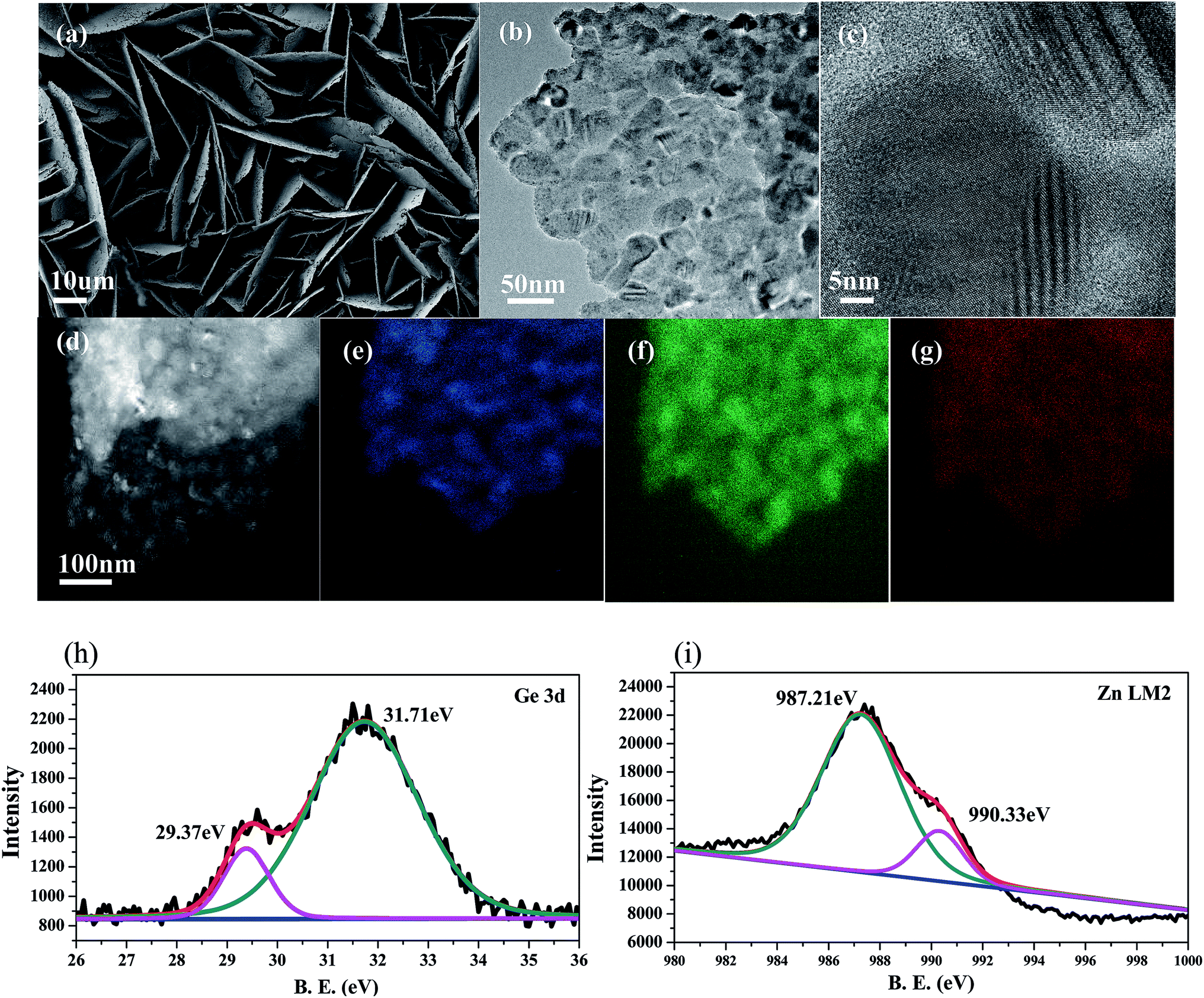 | ||
| Fig. 1 The structural and composite characterization of the sample. (a) SEM images of the as-synthesized sample. (b) Bright field TEM image. (c) High resolution TEM image. (d–g) EDS mapping points to the elements distribution of Ge, Zn and O. (h and i) XPS analysis of the sample corresponding to the Ge 3d and ZnLM2 signals, respectively. | ||
The field electron emission properties of the as-synthesized sample were measured in a vacuum chamber at a pressure of 10−7 torr at room temperature. Column-shaped stainless-steel probes with radii of 0.2 mm were used as the anode, as previously demonstrated in detail.21,22 The fresh sample grown on graphite substrate was used as the cathode, which was stuck to a Cu plate by double-sided conductive carbon tape. In this condition, electrons can be easily transported to the micro-nano structures through the conductive graphite substrate and the carbon tape. In the measuring circuit, the emission current was directly determined using a Keithley 6485.
Before measurement, the distance between the anode and the cathode was adjusted to be 200 μm. Then a series of voltage and current values was recorded, which is shown in the form of a J–E curve as in Fig. 2(a). The sample displayed very good field emission properties with electron emission tune-on (Eto) and threshold fields (Ethr) of 4.66 V μm−1 and 7.9 V μm−1, respectively, which are defined to be the macroscopic electric fields required to generate a current density of 10 μA cm−2 and 10 mA cm−2, respectively. According to the curve, the current density J shows a very steep increase along with the electric field E. The J value is as high as ∼30 mA cm−2 with an electric field of 9.0 V μm−1, which demonstrates the high field enhancement factor. Although the resulted Eto value is not fascinating enough comparing to some cold cathode emitters,23,24 the large current-emission capability at low electric field is amazing, declaring the uniqueness of it. This performance is even better than most nanotips.25,26 We believe the Ge dopant plays an important part in the enormously improved FE performance. It works effectively with several available mechanisms.
 | ||
| Fig. 2 FE investigation of the Ge doped ZnO nanosheets. (a) Typical J–E curve; the inset is the magnified data at the low emission current region. (b) The F–N relationship corresponding to the J–E curve; the inset is the experimental illustration. (c) Electron emission illustration of the sample. | ||
Firstly, the introduction of Ge elements in high concentration by occupying Zn sites in the lattice would produce large amounts of itinerant electrons, which contribute a lot to improving the conductivity of the structures.27 This helps to establish a smooth circuit for electrons. Furthermore, the high density of Ge impurity in the ZnO lattice results in a lower work function than pure ZnO, which is helpful to promote electron emission under an external field. On the other hand, the self-assembled free-standing 2D micro–nano units serve as a nanoparticle-based host for an electron source, in which several advantages are integrated together. For example, the sub-20 nm nanoparticles act as natural tips for electron emission with a very large field enhancement factor (β). Except for the nanosheet edges, the whole lateral parts of the structures are ready to contribute to the emission as a result of the ragged surface. These points, i.e. high conductivity, large emission area and large β, demonstrate the advantages of the novel structures. As exposed by XPS analysis, a little pure Ge exists in the sample. As characterized by TEM and analyzed in the growth part, we hypothesized that Ge may be distributed on the surface of the ZnxGe1−xO particles in an amorphous state, because we did not find Ge nanoparticles despite much effort having been made.18 As is well recognized, Ge has very large Bohr exciton radius (∼24 nm) and low work function, which is to say that both the confinement effect and low surficial potential barrier would enhance the electron emission enormously. Noticeably, a Ge composite between adjacent ZnxGe1−xO particles would also provide a smooth electron transport channel.
Herein, we would like to analyze the J–E relation using the Fowler–Nordheim (F–N) model in order to give analytical and semi-quantitative data for assessing the FE capability of the novel material. According to typical F–N theory, the field emission current J can be expressed in the following form:28

The PL spectra of Ge doped ZnO multi-crystalline nanosheets were acquired using μ-PL test technology assembled with a 325 nm HeCd laser.31 The inset of Fig. 3(a) displays the optical photograph of the nanosheet used for the experiment recorded from the CCD assembled on the confocal microscope. As shown in Fig. 3(a), the spectra are surprisingly dependent on the excitation power applied. In detail, the main NBE peak is located at 379.5 nm when 0.1% I0 was used, while the value is 412.5 nm if I0 was applied to excite the sample. At the same time, the intermediate powers result in different emission features, i.e. 1% (383.3 nm), 10% (383.9 nm), 30% (390.8 nm), and 60% (398.6 nm). Noticeably, the defect-related green emission is stable at 522 nm and 550 nm, as shown in Fig. 3(b). Herein, we mainly focus our consideration on the NBE emission. Actually, the excitation power-dependent redshift has been investigated in detail.32,33 Yang and Li proposed that laser-induced local heating effect is the origin of the phenomenon and the established theoretical model agrees well with the experiment results.34 However, Rao et al. pointed out that the heating effect alone cannot explain the observed shift in the PL with the variation in excitation intensity, based on the fact that some samples were free of spectrum shift and the same phenomenon was even found in a liquid nitrogen environment.12 Here in our case, all of the samples exhibit similar performance and a redshift occurs even at 77 K. Based on the careful characterization of the sample, we investigated the spectral behavior depending on changes to the excitation power and temperature.
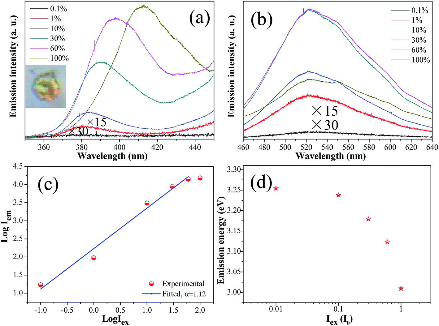 | ||
| Fig. 3 The room-temperature PL investigation of a single unit. (a) The PL spectra of the sample in the NBE region; the inset is the optical image of the nanosheet used. (b) Corresponding PL spectra in the visible region. (c) The relationship between Iem and Iex extracted from (a). (d) The excited power-dependent emission energy. | ||
According to the radiative recombination rate model, the PL intensity, Iem, depends on the excitation laser Iex, as:
| Iem = η(Iex)α |
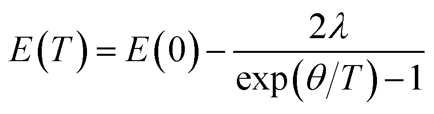
To get some insight into this issue, temperature-dependent excitation was carried out upon another unit in the temperature range of 77–300 K, as shown in Fig. 4. Fig. 4(a) shows the T-dependent emission energy of the sample at various excitation powers and Fig. 4(b) points to the power-dependent emission energy at various temperatures, in which we can analyze the influence of temperature and power, respectively. Firstly, the curves were fitted according to the band gap renormalization model, also known as the electro–photon interaction, which results in the expression as:
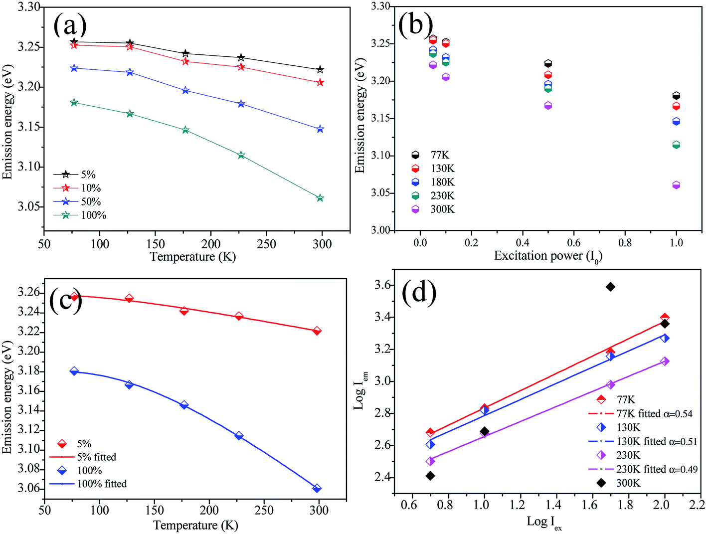 | ||
| Fig. 4 The temperature-dependent PL spectra. (a) The temperature-dependent emission energy at various powers. (b) The excitation power-dependent emission energy at various temperatures. (c) The fitted results according to band gap renormalization model. (d) The relationship between Iem and Iex at different temperatures. | ||
The excitation power-dependent PL energy as shown in Fig. 4(b) can further support this conclusion, in which the PL displays an obvious redshift with the increase of excitation power even though the temperature remain unchanged. Noticeably, the trend is more distinguished at elevated temperatures. These analyses indicate that the redshift resulted from the synergetic effect of temperature and excitation power. Additionally, the η values below 220 K are more or less than 0.5, implying that free-to-bound or donor–acceptor transitions dominate. Alternatively, the values deviate from linear fitting at 300 K shown as the violet spots in Fig. 4(d), which is similar to in Fig. 3(c). It indicates that the PL are dominated by different combination mechanisms at alternative temperatures involving the complex indirect transitions resulted from the rich defect and impurity levels. However, we think the activation factor of these recombination mechanisms is temperature, including environmental and self-heating by the excited laser. At low laser powers when the excitation is far from saturation, the heating effect-induced redshift (band gap renormalization) may be dominant. The continuous increase of the excited density results in two consequences. Firstly, the free exciton recombination and the interband transitions are saturated. Secondly, the nonradiative transitions would be enhanced. As the laser power and environmental temperature increase, the active levels relax, deviating from the conduction band bottom.
However, we can't decide if these levels are from Ge dopant or intrinsic defects because impurities and native defects co-exist and interplay. For example, the enrichment of Ge atoms at the interface between crystal grains (according to previous characterization) would increase the density of electron trapping, because the electrons trapped at the interface state can be charge compensated by ionized Ge, which illustrates the fact that the defect-related green emission is more obvious than the NBE emission in our samples.
Conclusion
In conclusion, 2D Ge-doped ZnO nanostructures were synthesized by CVD method. The sample on graphite substrate exhibits good field electron emission properties with tune-on (Eto) and threshold fields (Ethr) of 4.66 V μm−1 and 7.9 V μm−1, respectively. The emission current is as high as 30 mA cm−2 at the E value of 9.0 V μm−1, which indicates the contribution of the small curvatures and rich spots of emitters. Such a good performance originates from the improved electron conductivity and the high density of emitters on the surface of the nanosheet. Additionally, a single unit displays temperature- and laser power-dependent PL performance. We attribute it to the band gap renormalization in the moderate excited condition. The local thermal energy provided by self-heating effect and environmental temperature drives the alternative recombination mechanism.Acknowledgements
This work was financially supported by the National Natural Science Foundation of China (11274392, U1401241, 51502353).References
- N. S. Xu and S. E. Huq, Novel Cold Cathode Materials and Applications, Mater. Sci. Eng., R, 2005, 48, 47–189 CrossRef.
- T. Akasaka, H. Gotoh, Y. Kobayashi and H. Yamamoto, Extremely narrow violet photoluminescence line from iltrathin InN single quantum well on step-free GaN surface, Adv. Mater., 2012, 24, 4296–4300 CrossRef CAS PubMed.
- L. Xu, Z. Jiang, Q. Qing, L. Q. Mai, Q. j. Zhang and C. M. Lieber, Design and Synthesis of Diverse Functional Kinked Nanowire Structures for Nanoelectronic Bioprobes, Nano Lett., 2013, 13, 746–751 CrossRef CAS PubMed.
- M. H. Huang, S. Mao, H. Feick, H. q. Yan, Y. Y. Wu, H. Kind, E. Weber, R. Russo and P. D. Yang, Room-Temperature Ultraviolet Nanowire Nanolasers, Science, 2001, 292, 1897 CrossRef CAS PubMed.
- B. C. Cheng, Z. D. Zhang, H. J. Liu, Z. H. Han, Y. H. Xiao and S. J. Lei, Power- and energy-dependent photoluminescence of Eu3+ incorporated and segregated ZnO polycrystalline nanobelts synthesized by a facile combustion method followed by heat treatment, J. Mater. Chem., 2010, 20, 7821–7826 RSC.
- G. T. Dang, H. Kanbe, T. Kawaharamura and M. Taniwaki, Pulsed laser excitation power dependence of photoluminescence peak energies in bulk ZnO, J. Appl. Phys., 2011, 110, 083508 CrossRef.
- Y. Yang, H. L. Zhang, G. Zhu, S. Lee, Z. H. Lin and Z. L. Wang, Flexible Hybrid Energy Cell for Simultaneously Harvesting Thermal, Mechanical, and Solar Energies, ACS Nano, 2013, 7, 785–790 CrossRef CAS PubMed.
- Y. Yang, K. C. Pradel, Q. S. Jing, J. M. Wu, F. Zhang, Y. S. Zhou, Y. Zhang and Z. L. Wang, Thermoelectric Nanogenerators Based on Single Sb-Doped ZnO Micro/Nanobelts, ACS Nano, 2012, 6, 6984–6989 CrossRef CAS PubMed.
- H. Yan, J. Johnson, M. Law, R. He, K. Knutsen, J. R. McKinney, J. Pham, R. Saykally and P. D. Yang, ZnO Nanoribbon Microcavity Lasers, Adv. Mater., 2003, 15, 1907 CrossRef CAS.
- D. J. Gargas, M. C. Moore, A. Ni, S. W. Chang, Z. Y. Zhang, S. L. Chuang and P. D. Yang, Whispering Gallery Mode Lasing from Zinc Oxide Hexagonal Nanodisks, ACS Nano, 2010, 4, 3270–3276 CrossRef CAS PubMed.
- M. Karaliunas, E. Kuokstis, S. Y. Ting, J. J. Huang and C. C. Yang, Temperature dependent double blueshift of photoluminescence peak position in MgZnO epitaxial layers, J. Appl. Phys., 2014, 116, 123501 CrossRef.
- T. P. Rao, G. K. Goswami and K. K. Nanda, Detailed understanding of the excitation-intensity dependent photoluminescence of ZnO materials: Role of defects, J. Appl. Phys., 2014, 115, 213513 CrossRef.
- T. Schmidt, K. Lischka and W. Zulehner, Excitation-power dependence of the near-band-edge photoluminescence of semiconductors, Phys. Rev. B: Condens. Matter Mater. Phys., 1992, 45, 898–8994 CrossRef.
- H. A. Rafaie, R. M. Nor and Y. M. Amin, Magnesium doped ZnO nanostructures synthesis using Citrus aurantifolia extracts: Structural and field electron emission properties, Mater. Express, 2015, 5, 226–232 CrossRef CAS.
- D. Kim, M. Lee, J. Park, M. Kim and T. Song, New Physics: Sae Mulli, 2015, 65, 730734 Search PubMed.
- E. D. Gasper, N. W. Duffy, J. Embden, L. Waddington, L. Bourgeois, J. J. Jasieniak and A. S. R. Chesman, Chem. Commun., 2015, 51, 12369 RSC.
- Z. Li, L. Xu, A. Abliz, Y. Hua, J. C. Li, Y. Shi, W. Liu and L. Liao, J. Disp. Technol., 2015, 11, 670–673 CrossRef CAS.
- Y. Sun, G. Z. Yang, H. Cui, J. Wang and C. X. Wang, ZnxGe1−xO 3D Micronano Structures with Excellent Performance as Anode Material in Lithium Ion Battery, ACS Appl. Mater. Interfaces, 2015, 7, 15230–15239 CAS.
- Y. Sun, H. Cui and C. X. Wang, Step-edge induced ordered growth: targeting to assemble super long horizontal nanowire alignment in large-scale, Phys. Chem. Chem. Phys., 2013, 15, 11808–11813 RSC.
- Y. Sun, H. Cui, S. X. Jin and C. X. Wang, Eutectic solidification applied to nanofabrication: a strategy to prepare large-scale tungsten carbide nanowalls, J. Mater. Chem., 2012, 22, 16566 RSC.
- Y. Sun, H. Cui, L. Gong, J. Chen, P. K. Shen and C. X. Wang, Field nanoemitter: One-dimension Al4C3 ceramics, Nanoscale, 2011, 3, 2978–2982 RSC.
- Y. Sun, H. Cui, L. Gong, J. Chen, J. C. She, Y. M. Ma, P. K. Shen and C. X. Wang, Carbon-in-Al4C3 Nanowire Superstructures for Field Emitters, ACS Nano, 2011, 5, 932–941 CrossRef CAS PubMed.
- N. G. Shang, P. Papakonstantinou, P. Wang, A. Zakharov, U. Palnitkar, I. N. Lin, M. Chu and A. Stamboulis, Self-Assembled Growth, Microstructure, and Field-Emission High-Performance of Ultrathin Diamond Nanorods, ACS Nano, 2009, 3, 1032–1038 CrossRef CAS PubMed.
- Y. B. Li, Y. Bando and D. Golberg, ZnO Nanoneedles with Tip Surface Perturbations: Excellent Field Emitters, Appl. Phys. Lett., 2004, 84, 3603–3605 CrossRef CAS.
- J. Chen, S. Z. Deng, N. S. Xu, S. H. Wang, X. G. Wen, S. H. Yang, C. L. Yang, J. N. Wang and W. K. Ge, Field Emission from Crystalline Copper Sulphide Nanowire Arrays, Appl. Phys. Lett., 2002, 80, 3620–3622 CrossRef CAS.
- S. C. Shi, C. F. Chen, S. Chattopadhyay, K. H. Chen and L. C. Chen, Field Emission from Quasi-Aligned Aluminum Nitride Nanotips, Appl. Phys. Lett., 2007, 87, 073109–073111 CrossRef.
- Y. B. Lu, Y. Dai, M. Guo, L. Yu and B. B. Huang, Phys. Chem. Chem. Phys., 2013, 15, 5208–5214 RSC.
- R. H. Fowler and L. W. Nordheim, Electron Emission in Intense Electric Fields, Proc. R. Soc. A, 1928, 119, 173–181 CrossRef CAS.
- J. Zhou, N. S. Xu, S. Z. Deng, J. Chen, J. C. She and Z. L. Wang, Large-Area Nanowires Arrays of Molybdenum and MolybdenumOxide: Synthesis and Field Emission Properties, Adv. Mater., 2003, 15, 1835–1840 CrossRef CAS.
- Y. B. Li, Y. Bando and D. Golberg, ZnO Nanoneedles with Tip Surface Perturbations: Excellent Field Emitters, Appl. Phys. Lett., 2004, 84, 3603–3605 CrossRef CAS.
- Y. Sun, Y. Z. Chen, C. R. Ding, G. W. Yang, Y. M. Ma and C. X. Wang, One-dimensional Al4O4C ceramics: a new type of blue light emitter, Sci. Rep., 2013, 3, 1749 Search PubMed.
- A. Gupta, M. Omari and N. Kouklin, Spectral investigation of carrier recombination processes in ZnO nanorods at high temperatures, J. Appl. Phys., 2008, 103, 124312 CrossRef.
- X. B. Chen, J. Huso, J. L. Morrison and L. Bergman, The properties of ZnO photoluminescence at and above room temperature, J. Appl. Phys., 2007, 102, 116105 CrossRef.
- Y. L. Yang, H. W. Yan, Z. P. Fu, B. F. Yang, L. S. Xia, Y. D. Xu, J. Zuo and F. Q. Li, Photoluminescence Investigation Based on Laser Heating Effect in ZnO-Ordered Nanostructures, J. Phys. Chem. B, 2006, 110, 846–852 CrossRef CAS PubMed.
- T. Schmidt and K. Lischka, Excitation-power dependence of the near-band-edge photoluminescence of semiconductors, Phys. Rev. B: Condens. Matter Mater. Phys., 1991, 45, 8989–8994 CrossRef.
| This journal is © The Royal Society of Chemistry 2017 |