
 Open Access Article
 This Open Access Article is licensed under a
 Creative Commons Attribution 3.0 Unported Licence
Effect of samarium and vanadium co-doping on structure, ferroelectric and photocatalytic properties of bismuth titanate†
E. Venkata Ramana *a,
N. V. Prasad*b,
David Maria Tobaldic,
Janez Zavašnikd,
M. K. Singhe,
María Jésus Hortigüelae,
M. P. Seabrac,
G. Prasadb and
M. A. Valentea
*a,
N. V. Prasad*b,
David Maria Tobaldic,
Janez Zavašnikd,
M. K. Singhe,
María Jésus Hortigüelae,
M. P. Seabrac,
G. Prasadb and
M. A. Valentea
aI3N-Aveiro, Department of Physics, University of Aveiro, Aveiro-3810 193, Portugal. E-mail: venkataramanaesk@rediffmail.com
bMaterials Research Laboratory, Department of Physics, Osmania University, Hyderabad-500 007, India. E-mail: nvp_phys@osmania.ac.in; nvp1969@rediffmail.com
cDepartment of Materials and Ceramics Engineering/CICECO, University of Aveiro, Aveiro-3810 193, Portugal
dJožef Stefan Institute, Centre for Electron Microscopy and Microanalysis, Jamova cesta 39, 1000 Ljubljana, Slovenia
eCentre for Mechanical Technology and Automation (TEMA), Department of Mechanical Engineering, University of Aveiro, Aveiro-3810 193, Portugal
First published on 2nd February 2017
Abstract
We performed a systematic analysis of the structure, ferroelectric and photocatalytic activities of Sm and V co-doped Bi4Ti3O12 (SBVT) ceramics. The formation of 3-layered Aurivillius structure and chemically induced strain of SBVT were analyzed by SEM and HRTEM studies. From the results of structural refinements, temperature dependent XRD and Raman spectra we found that SBVT has a distorted orthorhombic structure and transforms to tetragonal in the temperature range of 475–600 °C. Raman modes of Bi sites experience the phase transition earlier compared to torsional bending modes of BO6 octahedra. From the results of polarization and piezoelectric strain measurements, we found that SBVT exhibits superior ferroelectric characteristics as well as improved S33 (0.02 × 10⁻³) compared to other rare-earth doped Bi4Ti3O12 materials reported in the literature. SBVT exhibited fatigue endurance up to 108 switching cycles. Such a behavior is attributed to the structural distortions due to the smaller ionic radius of Sm3+ and reduced oxygen vacancies. Local piezoresponse measurements demonstrated imprint characteristics of ferroelectric domains. Furthermore, we assessed the photocatalytic (PC) activity of SBVT – for the first time – in the gas–solid phase, monitoring the degradation of nitrogen oxides (i.e. NO + NO2). Results demonstrated that SBVT was photocatalytically active in the solar spectrum, being able to degrade NOx at ppb level concentration, and exhibited a very stable PC activity (five consecutive PC runs), proving itself suitable for reuse.
1. Introduction
Bismuth layered perovskites of the Aurivillius family have received a lot of attention because of their potential applications in non-volatile memory, electro-optic devices, and microelectromechanical systems.1–4 Aurivillius phases are characterized by the formula: (Bi2O2)2+(Am−1BmO3m+1)2−, where A- and B-sites are in cuboctahedral and octahedral coordination, respectively. The integer m represents the number of octahedral layers.5,6 The spontaneous polarization for even-layered Aurivillius phases is along the a-axis while for odd-layered compounds like Bi4Ti3O12 (BTO), it is within the a–c plane, with the major polarization along the a-axis. BTO with monoclinic structure (B1a1) has been regarded as a promising candidate for memory devices due to its high Curie temperature (TC ∼ 675 °C) and large spontaneous polarization (PS ∼ 50 µC cm−2). However, it was found that rare-earth (such as La and Nd) doped BTO films are fatigue-free compared to BTO. Although tremendous research is being made on La doped BTO, the plausible mechanism of La role is required for the complete commercialization point of view. In addition to rare-earth doping, substitution of V5+ for Ti4+ helps to enhance dielectric and ferroelectric properties due to the increased rattle space inside the oxygen octahedra.7,8 In view of improved ferroelectric properties in A- and B-site doped BTO new rare-earth doped materials are being studied for their applications in memory.Apart from the use in non-volatile memories, BTO based materials have recently attracted the attention of the scientific community for photovoltaic (PV) and photocatalytic (PC) applications. Aurivillius materials are considered as alternatives to conventional TiO2 – based photo catalysts,9 mainly because, in these materials, bismuth shifts the absorption into the visible range thanks to hybrid Bi 6s–O 2p orbitals in the valence band10 and an extended separation of the photo-generated pair e−/h+.11 BTO films grown on FTO substrate by a sol–gel technique, were reported to show a maximum PV conversion efficiency of 0.00026%.12 In a recent study Bi3.25La0.75Ti3O12 thin film grown on p-type silicon with energy bandgap of 3.8 eV was found to exhibit strong visible-light photovoltaic effect with high photoresponsivity.13 He et al.14 reported a strong photoresponse and photovoltaic performance for BTO/FTO thin films that can be modulated either by applying different bias voltages or through different poling states.14 Chen et al.,15 in a recent study showed that BTO nano-sheets exhibited 79.2% of photo degradation efficiency of rhodamine B under 90 min of sunlight irradiation, larger than that of conventionally calcined BTO. Cao et al.16 reported that BTO/TiO2 heterostructures exhibit higher degradation rate of rhodamine B (RhB) than the unmodified TiO2 submicron fibers under visible light. Such an effect was attributed to the extended absorption in the visible light region resulting from the BTO nano-sheets and the effective separation of photo generated carriers driven by the photo induced potential difference at the junction. Hou et al.17 reported the strong PC activity for a p–n junction photocatalyst of BTO nanofibers–BiOI nano-sheets.
In view of above reports it is understood that PC applications of BTO is still an emerging field. However, most of the reported literature dealt with BTO and PC activity uses organic dyes as pollutants to be degraded in the liquid–solid phase.18–22 On the contrary, in this research, modified BTO is used to degrade nitrogen oxides (NO & NO2) that are amongst the major atmospheric pollutants (both indoor and outdoor), being harmful to human beings23 and responsible for photochemical smog and acid rain;24,25 indeed, this is the first research of its kind to use BTO as a PC material working in the gas–solid phase against such harmful pollutants.
Based on the above salient work carried out on photocatalytic activity and rare-earth doped BTO for memory we synthesized Sm and V doped BTO ceramics. The chosen composition was Sm0.75Bi3.25Ti2.9625V0.03O12 (SBVT). We performed detailed structural studies by in situ X-ray diffraction, Raman spectroscopy and transmission electron microscopy. The photocatalytic activity (PCA) of SBVT material was assessed for the first time in the gas–solid phase, monitoring the degradation of nitrogen oxides. Results showed that SBVT material was photocatalytically active in the solar spectrum.
2. Experimental
SBVT ceramics were synthesized by the conventional solid state reaction method. High-purity (99.9%) starting materials Bi2O3, Sm2O3, TiO2 and V2O5 were mixed in stoichiometric ratio and milled for 12 h in ethanol media. The resulting slurry was dried and calcined at 900 °C for 2 hours. The powder obtained was again milled for 24 h and pressed under cold isostatic conditions, at 200 MPa, into cylindrical discs with 10 and 25 mm diameter. Final sintering was carried out at 1050 °C for 4 hours.The crystal structure of the specimens was analyzed using the X-ray diffraction (XRD). Prior to the measurements, ceramic discs were powdered and annealed at 400 °C for 1 h to release strains. The data for structural characterization were collected using a Phillips X-ray diffractometer equipped with a fast RTMS detector and graphite monochromated Cu Kα radiation source (45 kV and 40 mA, 2θ range of 5–110°, a virtual step scan of 0.01° and virtual time per step of 798 s). Rietveld refinements on the full profile fitting of the XRD patterns were accomplished using the GSAS-EXPGUI software suite.26,27 High temperature XRD (HTXRD) scans, in the 2θ range 10–80°, were done in the temperature range 22–700 °C, operated with an accuracy of ±1 K using a Pt–Rh thermocouple directly attached to the sample holder. Raman spectroscopic measurements were made using a micro-Raman spectrometer (Horiba Jobin Yvon) with a 532 nm excitation laser, an edge filter for Rayleigh line rejection, and a CCD detector. The laser was focused on the sample to a spot size of ∼2 mm using a 50× objective lens in the temperature range 296–500 K, using a Linkam TC91 stage (Linkam Scientific Instruments Ltd., UK).
Surface morphology was evaluated by scanning electron microscopy (SEM, VEGA 3, Tescan). The structure and chemistry of the samples were studied using a 200 kV transmission electron microscope (TEM; JEM-2100, Jeol Inc., Japan) equipped with LaB6 filament and energy-dispersive X-ray spectrometer (EDS). The micrographs were recorded with high-resolution slow-scan CCD camera (Orius DC1000, Gatan Inc.). Samples were scratched from the sintered disc and directly transferred on commercially available Cu grids (200 mesh Cu holey carbon, SPI Supplies/Structure Probe, Inc.) without dispersing in water, to avoid further alteration of the samples.
For electrical measurements gold electrodes were sputtered on polished ceramic specimens. Polarization–electric field hysteresis loops were measured using the hysteresis loop tracer TF-Analyzer (aixACCT). The dependence of longitudinal strain (S) on electric field (E) was measured at a frequency of 0.1 Hz in a silicone oil bath using a linear variable differential transformer. Dielectric measurements were performed using HP 4194 A analyzer in the frequency range (100 Hz to 1 MHz) from room temperature to 600 °C. Local piezoresponse was visualized using a commercial scanning probe microscope (Ntegra Prima, NT-MDT) equipped with an external lock-in amplifier (SR 830, Stanford Research) and a function generator (Yokogawa, FG 120). Here, we used commercial phosphorus doped Si probes (NANOSENSORS) with a radius of curvature R < 10 nm, resonance frequency 13 kHz and spring constant (k) = 0.2 N m−1.
X-ray photoelectron spectra (XPS) were acquired in an ultra-high vacuum (UHV) system with a base pressure of 2 × 10⁻¹⁰ mbar equipped with a hemispherical electron energy analyzer (SPECS Phoibos 150), a delay-line detector and a monochromatic Al Kα (1486.74 eV) X-ray source. High resolution spectra were recorded at normal emission take-off angle and with a pass-energy of 20 eV. For XPS measurements the powder sample was diluted in milli-Q water and a thin film was deposited on a silicon wafer by drop coating. Afterwards it was annealed under UHV conditions at approximately 400 K to remove surface contamination and water. C 1s spectrum was measured as reference for binding energy (BE) correction. The main peak of C 1s spectrum, assigned to hydrocarbons from adventitious contamination, was referenced to 285.0 eV.
Diffuse reflectance spectroscopy (DRS) was used to investigate the optical behavior of the synthesized SBVT specimen, and to obtain information of the apparent optical bandgap (Eg) of the specimen, as this is a key-point in photocatalytic applications. Spectra were acquired in reflectance mode using a Shimadzu UV 3100 (JP) spectrometer, equipped with an integrating sphere made of BaSO4, in the UV-Vis range (850–250 nm), with 0.2 nm resolution, using Spectralon® as white reference material.
The specific surface area (SSA) was evaluated by the Brunauer–Emmett–Teller (BET) method (Micromeritics Gemini 2380, US) using N2 as the adsorbate gas, on samples degassed at 120 °C. Pore volume (desorption cumulative pore volume, DCPV) and pore size distribution were estimated through the Barrett–Joyner–Halenda (BJH) method.
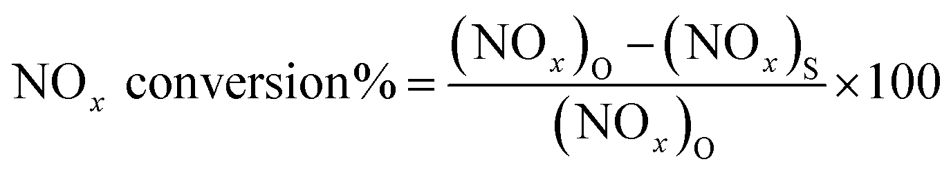
Photocatalytic activity tests were assessed in the gas–solid phase monitoring the abatement of nitrogen oxides (i.e. NO + NO2 = NOx), that are amongst the major atmospheric pollutants.25,28 The reactor employed worked in continuous conditions and has been previously described in detail by the authors.29,30 It is composed of a stainless steel cylinder (35 L in volume); its top was sealed and covered with a Pyrex glass window to allow the light to reach the photocatalyst placed inside it. The solar lamp light source (Osram Ultra-Vitalux, 300 W) was placed 50 cm above the photocatalyst, so as to have a light intensity entering the reactor, and reaching the surface of the photocatalyst, equal to 8 W m−2 in the UVA range (315–400 nm), and 50 W m−2 in the visible-light range (400–800 nm) – values measured with a radiometer, Delta OHM, HD2302.0 (IT), equipped with visible and UVA probes. Samples were prepared in the form of a thin layer of powder, with a constant mass (∼0.10 g), and thus approximately constant thickness, in a 6 cm diameter Petri dish (irradiated surface ∼ 28.3 cm2). The tests were performed at 27 ± 1 °C (temperature inside the reactor) with a relative humidity (RH) of 31%. These parameters – controlled by a thermocouple that was placed inside the chamber, and a humidity sensor placed in the inlet pipe – remained strictly stable throughout the tests. The outlet concentration of the pollutant gas was measured using a chemiluminescence analyzer (AC-31 M, Environment SA, FR). After having placed the photocatalyst inside the reactor and covered the glass window, the inlet gas mixture (prepared using cylinders with synthetic air and NOx gas) was allowed to flow until it reached a stable concentration of 200 ppb (two mass flow controllers were used to prepare a mixture of air with this concentration of NOx). Once the desired concentration of 200 ppb was reached and stabilized inside the reactor, the window glass was uncovered, the lamp turned on, and the photocatalytic reaction was presumed to start. Control photolysis experiment was assessed prior to run a real photocatalytic test, and this proved to be negligible, as reported in Fig. S1.† The photocatalytic efficiency was evaluated as the ratio of the removed concentration of NOx, and the conversion rate (%) of the initial NOx concentration was calculated as:
3. Results and discussion
Fig. 1 shows the XRD θ–2θ scan of SBVT ceramic. The synthesis protocol resulted in high purity Aurivillius phase whose reflections can be well-indexed to the BTO with B2cb(41) space group32 despite some minor shifting, overlapping and intensity-inconsistency. In order to find the effect of simultaneous Sm and V doping at A and B sites of BTO we performed Rietveld refinement on full profile fitting of the XRD patterns, accomplished using the GSAS-EXPGUI software suite.26 The starting atomic parameters for the orthorhombic BTO, described by the space group (SG) B2cb, were taken from the previous report of Hervoches and Lightfoot.32 The following parameters were refined: scale-factors and zero-point; the background profile was modelled using a tenth order shifted Chebyshev polynomial function; unit cell parameters and sample displacement effects. The profile was modelled using a pseudo-Voigt function and one Gaussian (GW) and two Lorentzian (LX and LY) terms, as well as peak correction for asymmetry were used to model it. Moreover, preferred orientation along [001] was also refined, adopting the March–Dollase approximation.33 Atomic positions and isotropic displacement parameters (Uiso) were refined too; the sum of the occupancies of Bi and Sm was constrained to the unity in all the refinements. Furthermore, the same atomic positions and Uiso were given to these two atoms, and restrained to be identical. As per Ti and V, this latter atom was not considered in the structural refinement, because of its tiny amount in the BTO, and also because it is difficult to differentiate between Ti and V due to their similar scattering factors. Consequently, it has to be stressed that the refined titanium atomic positions, Uiso, and occupancies, are actually the sum of Ti plus V. Once the bond lengths and bond angles were calculated from the listing of distances and bond angles from GSAS, they were used to obtain a 3D rendering of the orthorhombic phase, via the VESTA software package.34 Also, the distortion index (D), quadratic elongation (QE) and bond angle variances (BAV) of the TiO6 octahedral sites in the orthorhombic phase were calculated, according to the formalisms of Baur,35 and Robinson et al.,36 respectively. The unit cell parameters, unit cell volume, Rietveld agreement factors and crystal structural data are listed in Tables 1–3.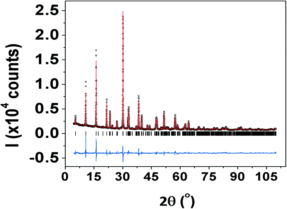 | ||
| Fig. 1 Rietveld graphical output of SBVT. The black open squares represent the observed pattern, the continuous red line represents the calculated pattern, and the difference curve between the observed and calculated profiles is given by the blue continuous line plotted below. The positions of the reflections are indicated by the small black vertical bars. | ||
| Crystallographic system | Orthorhombic |
|---|---|
| a Lattice parameters of BTO were1 a = 5.4444(1) Å, b = 5.4086(1) Å, c = 32.8425(6) Å and V = 967.1 Å3. | |
| Space group | B2cb |
| a (Å) | 5.4149(2) |
| b (Å) | 5.3974(2) |
| c (Å) | 32.8194(7) |
| Unit cell volume (Å3) | 959.19(4) |
| No. of reflections | 687 |
| No. of variables | 17 |
| χ2; RF2; Rwp | 4.94; 8.14%; 6.46% |
| Atom | x | y | z | U(iso)a Å2 | Occupancy |
|---|---|---|---|---|---|
| a Given as 100 × Uiso.b To be intended as the sum of Ti plus V. | |||||
| Bi(1) | 0.024(3) | 0.995(2) | 0.066(4) | 2.97(4) | 0.68(1) |
| Bi(2) | 0.021(1) | 0.012(2) | 0.212(2) | 1.32(3) | 0.82(1) |
| Sm(1) | 0.024(3) | 0.995(2) | 0.066(4) | 2.97(5) | 0.32(1) |
| Sm(2) | 0.021(1) | 0.012(2) | 0.212(2) | 1.32(2) | 0.18(1) |
| Ti(1) | −0.013(1) | 0 | 1/2 | 0.20(1) | 1b |
| Ti(2) | 0.005(1) | 0.002(1) | 0.373(1) | 0.36(1) | 1b |
| O(1) | 0.322(3) | 0.265(2) | 0.007(2) | 7.27(2) | 1 |
| O(2) | 0.265(3) | 0.263(1) | 0.249(1) | 0.70(1) | 1 |
| O(3) | 0.086(4) | 0.064(3) | 0.441(1) | 0.98(1) | 1 |
| O(4) | 0.052(3) | 0.945(2) | 0.319(1) | 3.51(8) | 1 |
| O(5) | 0.284(4) | 0.253(2) | 0.111(1) | 0.47(7) | 1 |
| O(6) | 0.217(3) | 0.210(3) | 0.856(1) | 0.73(2) | 1 |
| Ti1 | Distance |
|---|---|
| Ti(1)–O(1) × 2 | 2.22677(5) |
| Ti(1)–O(1) × 2 | 1.70044(4) |
| Ti(1)–O(3) × 2 | 2.05170(4) |
| Distortion index (D) | 0.0979 |
| Quadratic elongation (QE) | 1.0649 |
| Bond angle variance (BAV, deg2) | 180.06 |
| 〈Ti(1)–O〉 | 1.9929(1) |
| Ti2 | Distance |
|---|---|
| Ti(2)–O(3) | 2.28921(4) |
| Ti(2)–O(4) | 1.80452(3) |
| Ti(2)–O(5) | 2.09354(4) |
| Ti(2)–O(5) | 1.89963(4) |
| Ti(2)–O(6) | 1.97343(4) |
| Ti(2)–O(6) | 1.89270(4) |
| Distortion index (D) | 0.0667 |
| Quadratic elongation (QE) | 1.0370 |
| Bond angle variance (BAV, deg2) | 99.94 |
| 〈Ti(2)–O〉 | 1.9921(1) |
| Bi1 | Distance |
|---|---|
| Bi(1)–O(1) | 2.91294(4) |
| Bi(1)–O(1) | 2.57267(4) |
| Bi(1)–O(1) | 2.90733(4) |
| Bi(1)–O(3) | 2.36255(7) |
| Bi(1)–O(3) | 2.40035(7) |
| Bi(1)–O(5) | 2.46972(4) |
| Bi(1)–O(5) | 2.38814(4) |
| Bi(1)–O(6) | 2.429(26) |
| 〈Bi(1)–O〉 | 2.555(3) |
| Bi2 | Distance |
|---|---|
| Bi(2)–O(2) | 2.25125(4) |
| Bi(2)–O(2) | 2.29677(4) |
| Bi(2)–O(2) | 2.41572(4) |
| Bi(2)–O(2) | 2.20710(3) |
| Bi(2)–O(4) | 2.55551(6) |
| Bi(2)–O(4) | 2.74120(7) |
| 〈Bi(2)–O〉 | 2.411(1) |
| Bond | Angle (°) |
|---|---|
| Ti(1)–O(1)–Ti(1) | 153.3(1) |
| Ti(1)–O(3)–Ti(2) | 147.9(1) |
| Ti(2)–O(5)–Ti(2) | 148.2(1) |
| Ti(2)–O(6)–Ti(2) | 159.6(2) |
| Ti(1)–O(1)–Ti(1) | 153.3(1) |
The refined lattice parameters, as listed in Table 1, are a = 5.4149(2) Å, b = 5.3974(2) Å, c = 32.8194(7) Å and volume of 959.19(4) Å3 respectively. As compared to the undoped BTO the unit cell exhibited a shrinkage (0.542%, 0.21%, 0.07% and 0.82% decrease in a, b, c and volume respectively). This can be attributed to the smaller atomic radius of Sm3+ (1.079 Å) doped for Bi3+ (1.17 Å) and V5+ (0.55 Å) for Ti4+ (0.605 Å). The changes in unit cell dimensions in this study are similar to La3+, Pr3+, Nd3+ doped BTO.37 Structural changes of SBVT can be ascertained from the structural distortion parameters38 such as orthorhombicity [2(a − b)/(a + b)], tetragonal strain (c/a) and orthorhombic distortion (b/a) which are calculated to be 0.0032 (0.0066), 6.061 (6.0323) and 0.9967 (0.9934) respectively for SBVT(BTO). From these parameters, it can be seen that the addition of Sm and V has the effect of increased tetragonal strain and reduced orthorhombicity. As it is seen in Table 3, the (Ti1O6) octahedral site is more distorted than the (Ti2O6), in terms of D, QE, and BAV. This result is also visually depicted by the 3D rendering of SBVT in Fig. 2(a)–(c). Table 3 also reports the A–O bond length distances and B–O–B bond angles. It is clear that the average Bi1–O and Bi2–O distances 2.555(3) and 2.411(1) Å respectively, are shorter compared to that of BTO (2.749 Å and 2.682 Å).32 These results indicate that the BO6 octahedra are relaxed after doping with Sm3+ and V5+.
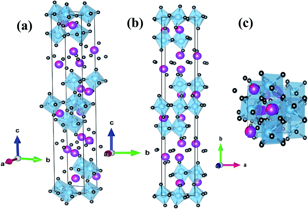 | ||
| Fig. 2 (a) 3D rendering of SBVT, in the ball-and-stick and polyhedron models, obtained using the structural data extracted from GSAS. (b) Along the a-axis direction; (c) along the c-axis direction. In the 3D renderings, the small dark grey spheres represent oxygen, the bigger light-blue sphere titanium, whilst the bigger violet spheres bismuth (in it is shown the fraction of samarium, magenta color). | ||
To track structural changes of SBVT with temperature we performed HTXRD measurements in the range 30–700 °C and the results are presented in Fig. 3(a)–(d). We observed a shift of characteristic (117) peak towards lower 2θ positions indicating the unit cell expansion with temperature (inset of Fig. 3(a)). With the increase in temperature the lattice reflections (020) and (200) become resolved around 475 °C and more distinguishable with further raise in temperature. The full width at half maximum (FWHM) of (020)/(200), obtained with pseudo – Voigt fittings and plotted against the temperature shows a gradual reduction with the temperature, more rapidly in the range 450–550 °C, indicates the orthorhombic–tetragonal (O–T) phase transition (Fig. 3(c)). Meanwhile, the reflections (220) and (1115) merge to a single peak with the increase in temperature (Fig. 3(b)). As compared to (220), the (1115) reflection shifts towards lower angle side more significantly and merges with (220) above 475 °C. It is known in BTO that the c-axis thermal expansion is larger than that of a- and b-axes.39 Hence the lattice reflections of c-axis shift substantially such that the (1115) and (220) merge to a single peak. The lattice parameters a, b and c of the orthorhombic structure increase linearly due to thermal expansion on heating while the b-axis exhibits a significant decrease around 475 °C and then approaches the a-axis of the tetragonal structure. This temperature can be considered as the Curie temperature (TC) which is ∼675 °C for BTO. As shown in Fig. 3(d), a- and c-axis show an increasing trend with temperature with no inflexion in the TC region. The orthorhombicity decreases with temperature and exhibits a slope change around TC. We did not achieve the equality a = b above 475 °C and no appearance or disappearance of XRD lines, indicating that the structure achieves a pseudo-tetragonal structure with the validity a0 ≈ b0 ≈ √2aT similar to that observed in BTO by Hirata and Yokokawa.39
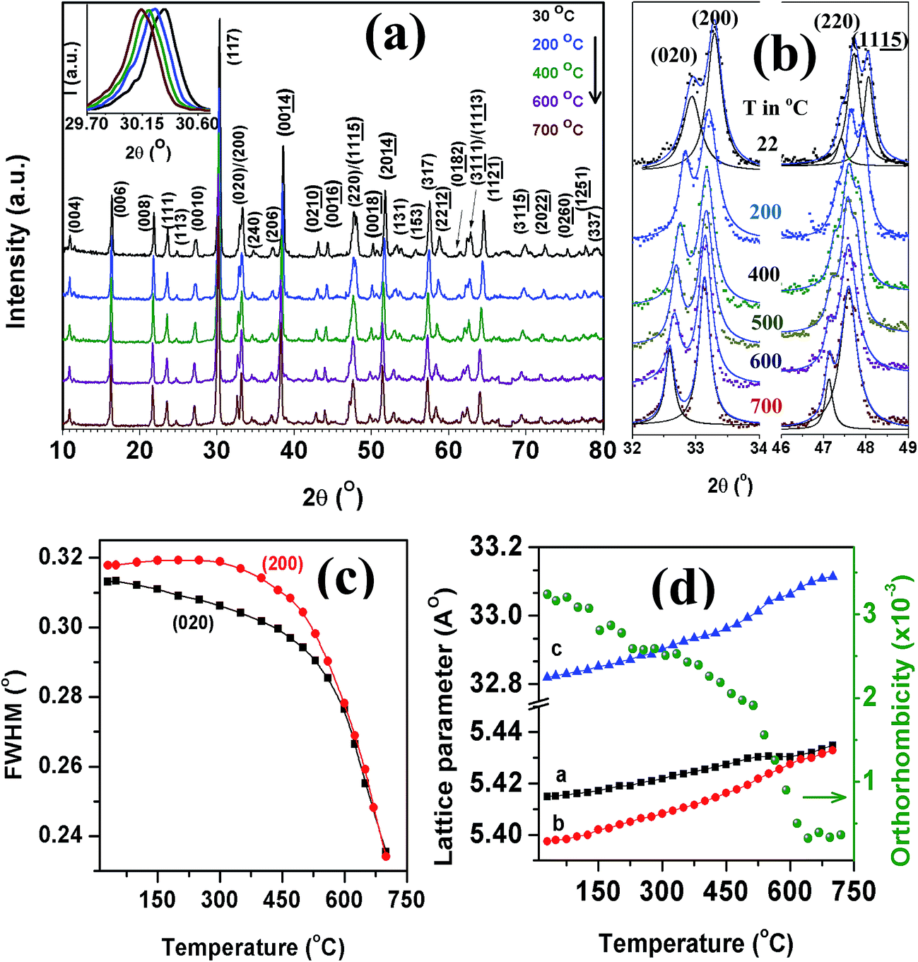 | ||
| Fig. 3 (a) HTXRD θ–2θ scans of SBVT sample measured in the 2θ range of 10–80°. Temperature dependent changes in the profiles of (020)/(200) and (220)/(1115) reflections (b), FWHM of (020)/(200) peaks (c) and unit cell parameters (d). Arrow in (d) indicates the phase transition temperature. | ||
Raman scattering is a sensitive technique to study lattice vibrational changes and site occupancies of doped ions. Orthorhombic BTO exhibits 24 Raman active modes: (6Ag + 2B1g + 8B2g + 8B3g)40–42 around 32, 57, 65, 90, 119, 148, 189, 228, 276, 332, 355, 449, 535, 562, 614 and 850 cm−1. However, as shown in Fig. 4(a) only 12 Raman modes are observed at room temperature, around 61, 91, 121, 156, 184, 250, 270, 335, 477, 511, 558, 628 and 851 cm−1, which is partially due to the possible overlap of the same symmetry vibrations or the weak features of some Raman modes. The high frequency peaks in the range 200–850 cm−1 originate from the internal vibrational modes of TiO6 octahedra, due to the large intragroup binding energy in the octahedra as well as lighter Ti4+ ions. The Raman modes at 270, 335, 558, 620, 851 cm−1 can be assigned to the A1g character, and the one at 477 cm−1 is related to B1g character.40 The peaks below 200 cm−1 are ascribed to two different Bi sites, the Bi2O2 layer and perovskite units. The mode at 65 cm−1 is assigned as a rigid-layer mode, which originates from Bi displacement in the Bi2O2 layers. The three modes of SBVT at 91, 121 and 156 cm−1, related to the Bi atoms in the perovskite units, have become diffused. The mode at 65 cm−1 of BTO is moved to lower frequency of 61 cm−1 due to structural hardening due to doping. This peak broadening was caused by the compositional inhomogeneity of the Bi atoms in the perovskite units. The blue shift observed in these modes is justified as Bi atoms are 1.39 times heavier than of Sm. The diffused low frequency modes in rare-earth doped BTO is reported to arise from the partial substitution of these atoms into (Bi2O2)2+ layers resulting in cation disorder in the (Bi2O2)2+ layers.43 However, in SBVT, based on the structural refinement results, it is clear that Sm is doped only at the Bi atomic sites of the (Bi2Ti3O10) units. Raman modes at 228, 332, 535, 614, 850 cm−1 of BTO were moved to high frequency side with doping, which is due to the simultaneous doping of lighter Sm and V atoms for Bi and Ti at A- and B-sites of the lattice respectively. The modes at 270 and 330 cm−1 correspond to the torsional bending of TiO6 octahedra and the modes at 558 and 851 cm−1 are related to the stretching of O–Ti octahedral chains between (Bi2O2)2+ layers. The Raman mode at 558 cm−1 is due to the combination of stretching and bending of the oxygen octahedra. From the results of Table 3 it is clear that the average Ti–O distance of SBVT is shorter and the octahedral tilting is reduced compared to BTO.32,44 The relaxation in structural distortions can also be seen from the orthorhombicity, which is 3.24 × 10⁻³ and 7.24 × 10⁻³ for SBVT and BTO respectively. These results match well with the significant shifting of Raman modes corresponding to octahedral tilting.
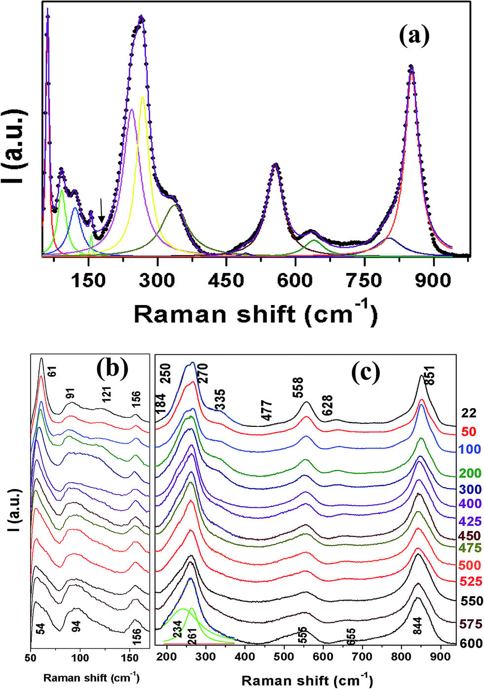 | ||
| Fig. 4 (a) Normalized Raman spectra of SBVT measured at room temperature. Temperature evolution of Raman spectra obtained in the frequency range 50–170 cm−1 (b) and 170–940 cm−1 (c). | ||
We measured temperature dependent Raman spectra in order to understand the effect of Sm and V doping on the phase transition behavior of BTO in the temperature range 22–600 °C and the results are shown in Fig. 4(b) and (c). The Raman modes around 61, 91 and 270 cm−1 exhibited a significant red shift as well as the weakening (large FWHM) with the increase in temperature. At the same time the room temperature modes at 121, 188, 335 and 628 cm−1 show a gradual weakening with temperature and disappear in the background above 450 °C. The intensity of high frequency modes shows a gradual decrease with the increase in temperature, which can be attributed to the decrease of optical penetration depth due to the increase of conductivity as well as the decrease in the deformation of TiO6 octahedra in the region of structural phase transition.45 From the HTXRD studies (Fig. 3(d)) the O–T transition is expected around 475 °C and the mode weakening/disappearance observed in Fig. 4 corroborates the phase transition. These effects at high temperature can be ascribed to the anharmonic phonon–phonon interactions of the lattice leading to thermal disorder.45 With the increase in temperature, there will be a change in bond length between oxygen and cations which is also responsible for the shifting of peak positions.
The phase transition of BTO is known to be around 675 °C and the drop in TC for SBVT can be understood by the following: the soft mode of BTO (around the wavenumber 30 cm−1) is determined by the difference between the short-range repulsive force and the coulombic force. The vanishing of the soft mode around O–T transition is the result of the balance between these two forces. The replacement of smaller Sm3+ for Bi3+ is expected to change the short-range force constant that may suppress the orthorhombic distortion and lower the phase transition temperature. The ferroelectricity of BTO-based materials is related to the displacement of Bi atoms along the a-axis with respect to the TiO6 octahedra.46 From Fig. 4(b) and (c) it is noteworthy that the modes corresponding to Bi atomic vibrations experience the phase transition earlier than those of octahedra as the bending of octahedra can be disturbed by the vibrations of Bi atoms in perovskite slabs.
The microstructure and crystallinity of SBVT samples were studied by electron microscopy. Fig. 5 shows the SEM micrograph of platelet-like crystals typical for Aurivillius – type structure, caused by the anisotropic structure. No secondary phases were detected, which is consistent with the XRD results. The samples are uniform and dense with randomly oriented platelets with an average size of 5 µm long and 0.9 µm thick. From the SEM cross-section we can conclude that the porosity is mainly located at grain boundaries. It has to be noted that an elongated morphology is reported to be favorable for photocatalytic applications.47 More detailed crystallographic studies were made by TEM. Fig. 6(a) shows a cross-sectional high-resolution transmission electron microscope (HRTEM) image of SBVT along the [110] zone-axis. The periodic fringes corresponding to the (Bi2O2)2+ layers are clearly observed, with a spacing of about 1.7 nm, approximated to c/2. The Fig. 6(b) shows the marked region that reveals the microstructure with fluorite-like (Bi2O2)2+ layers imaged as heavy lines interleaved by three perovskite-type layers. The SAED pattern in Fig. 6(c) further indicates the modulation of perovskite and (Bi2O2)2+ layers. These features clearly confirm the n = 3 structure of highly crystalline Aurivillius SBVT phase with no intergrowths caused by phase separation. Fig. 7(a) shows a HRTEM image of SBVT in [001] orientation parallel to the electron beam. The coherently spaced lattice fringes can be seen from the high magnification HRTEM image (Fig. 7(b)). The corresponding selected-area electron diffraction (SAED) pattern in Fig. 7(c) shows a near four-fold symmetry as the lattice parameters a and b are similar. The most intense spots in the pattern could be indexed to the room temperature orthorhombic cell with a and b parameters estimated to be ∼5.55 Å, which is in good agreement with XRD data. The chemical composition of SBVT studied by TEM-EDS (inset of Fig. 7(a)) reveals the presence of Sm, Bi, Ti, V and O atoms. From the atomic percentages we can confirm that the calculated cationic ratios match well with the expected ones.
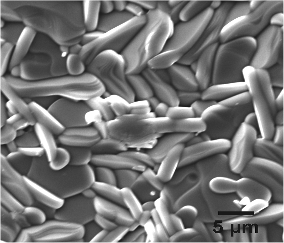 | ||
| Fig. 5 SEM micrograph of SBVT surface. Typical plate-like structure of the Aurivillius phase is visible on the edge of the crystallites as a set of lamellas. | ||
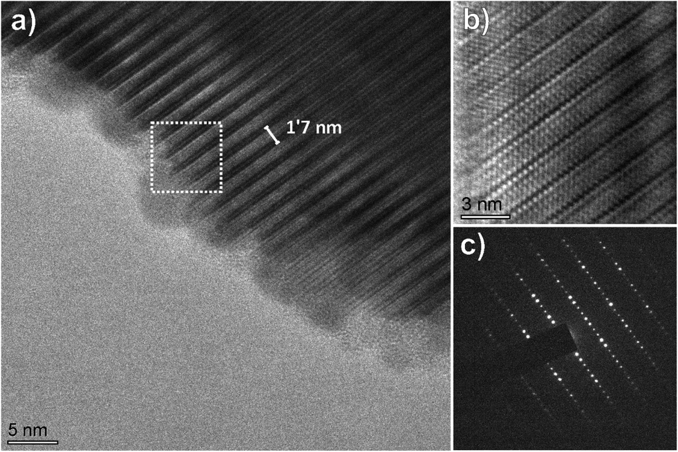 | ||
| Fig. 6 (a) TEM micrograph of SBVT sample along [110] zone axis, showing periodic alternations along c-axis. (b) HRTEM micrograph showing alteration of fluorite-type Bi-rich segments and intermediate perovskite layers; the image was ABS-filtered. (c) SAED pattern, according to single-crystal diffraction pattern showing extra reflection at 1/4 of the spacing of the prototype unit cell. Thus the periodicity of the modulation is 1-3-1, corresponding to 1 darker Bi-rich band, followed by 3 perovskite layers. | ||
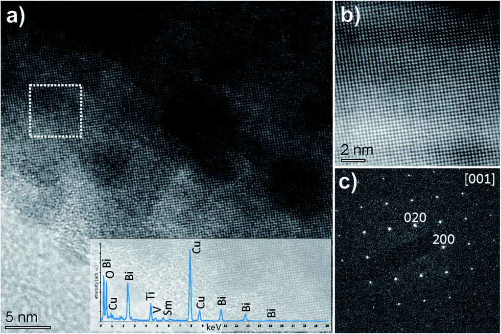 | ||
| Fig. 7 (a) HRTEM micrograph of SBVT in [001] parallel to the electron beam. Darker regions correspond to Bi exsolutions, which begin to grow only after seconds of exposure to the electron beam. The inset is EDS spectra recorded on the same region, conforming Sm, Bi, Ti, V and O composition, while Cu peak is an artefact from the Cu support grid. (b) ABSF filtered HRTEM micrograph of SBVT showing the coherent crystalline structure along a and b directions, without any periodic exsolutions. The corresponding SAED pattern (c) shows near four – fold symmetry; lattice parameters a and b being identical. The reflections marked as 020 and 200 correspond to d-values of approx. 5.55 Å, which is a good agreement with the values of 5.4149 and 5.3974 Å, obtained from XRD. | ||
Dielectric measurements were carried out in the temperature range 30–600 °C and the results are presented in Fig. S2.† With the increase in temperature dielectric constant (ε′r) and the loss (tan![[thin space (1/6-em)]](https://www.rsc.org/images/entities/char_2009.gif) δ) values increased steeply due to the increase in space charge polarization at lower frequencies. A clear TC can be seen from the ε′r measured at frequencies ≥100 kHz; at 100 kHz ε′r is 130, tanδ ∼ 0.003 and TC = 495 °C (Fig. S2a†). The tanδ also exhibits inflexion point at this temperature (Fig. S2b†), obeying the results of HTXRD and Raman studies. The onset of decay in FWHM vs. temperature curve of (200)/(020) XRD peak (Fig. 3(c)), observed around 490 °C, is thus related to TC.
δ) values increased steeply due to the increase in space charge polarization at lower frequencies. A clear TC can be seen from the ε′r measured at frequencies ≥100 kHz; at 100 kHz ε′r is 130, tanδ ∼ 0.003 and TC = 495 °C (Fig. S2a†). The tanδ also exhibits inflexion point at this temperature (Fig. S2b†), obeying the results of HTXRD and Raman studies. The onset of decay in FWHM vs. temperature curve of (200)/(020) XRD peak (Fig. 3(c)), observed around 490 °C, is thus related to TC.
The room temperature ferroelectric properties are depicted in Fig. 8. SBVT ceramic exhibited well-saturated P–E hysteresis loops without dielectric breakdown. The remanent polarization (2Pr) and coercive field (2EC) were 40.66 µC cm−2 and 145 kV cm−1, respectively. The saturation properties were characterized by the evolution of Pr, Pmax (PS) and EC as a function of applied field (Fig. 8(c)). The Pr and polarization PS shows a pronounced increase with the applied field, while a gradual increase was seen in the region of E ≈ 2EC. The polarization current (Fig. 8(b)) reaches a maximum value at the drive field of about EC (Fig. 8(c)) indicating the switching of ferroelectric domains. The Pr (& EC) values obtained in this study are comparable to recent literature on rare-earth doped BTO: 23.9 (125 kV cm−1) and 32.6 µC cm−2 (120 kV cm−1) for La and Nd doped BTO respectively,48 35 µC cm−2 (148 kV cm−1) for Bi3.25Pr0.75Ti2.97V0.03O12 ceramics,37 30.4 µC cm−2 (130 kV cm−1) for Bi3.25La0.75Ti2.97V0.03O12 ceramics,49 26 µC cm−2 (108 kV cm−1) for Bi3.15Nd0.85Ti2.97V0.03O12 (ref. 50) and 25 µC cm−2 (125 kV cm−1) for Bi3.25Sm0.75Ti2.97V0.03O12 ceramics.51 In BTO, the doping of rare-earth elements is supposed to reduce the oxygen vacancies and improve polarization and ferroelectric fatigue resistance. The enhanced polarization of SBVT compared to other rare-earth doped BTO is due to the smaller ionic size of Sm, resulting in larger structural distortion. The SBVT ceramic has larger BAV and tetragonal strain compared to BTO. At the same time the presence of higher valence V5+ for Ti4+ is effective to suppress the oxygen vacancies/vacancy complexes accumulated near domain boundaries resulting in domain pinning and reduced Pr.7,8
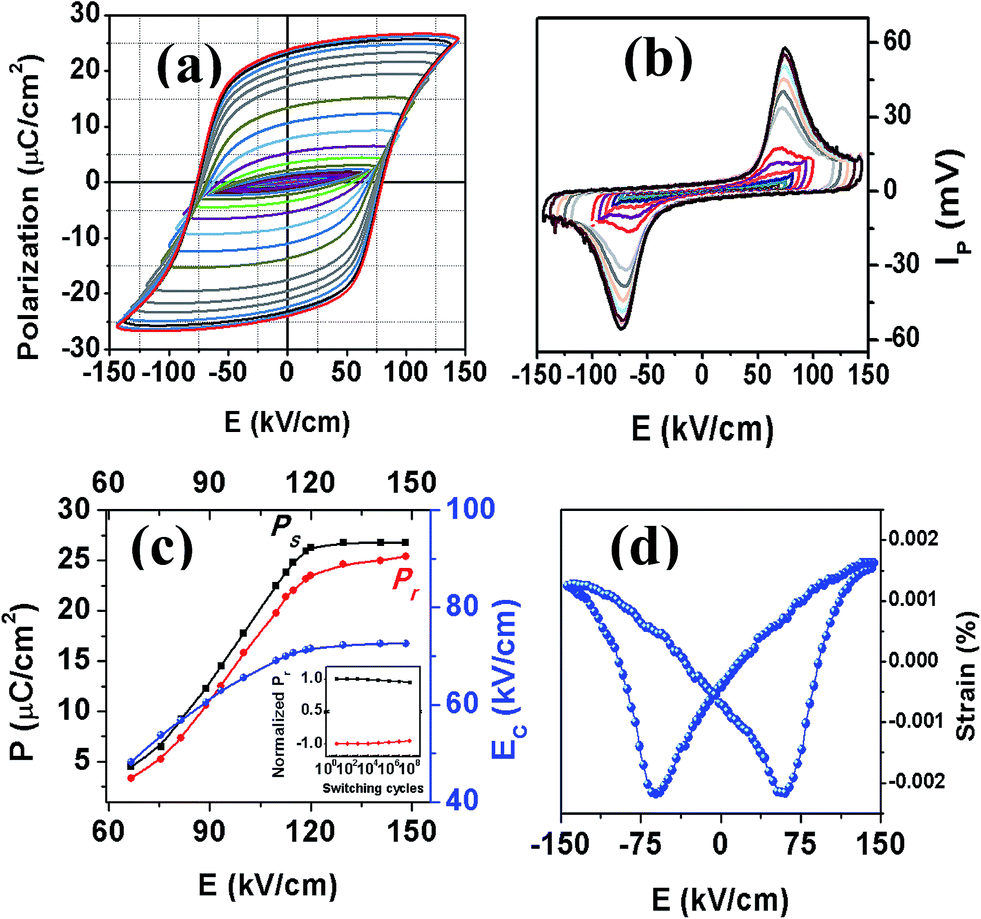 | ||
| Fig. 8 Room temperature polarization–electric field hysteresis loops of SBVT. Inset: electric field dependence of polarization current. (b) Pr vs. electric field. (c) Room temperature piezoelectric strain loop of SBVT at 1 Hz. Inset of (c): normalized Pr as a function of switching cycles. Comparison of P–E loops before and after 108 cycles is presented in fig. S4.† (d) Piezoelectric strain vs. electric field. | ||
The piezoelectric strain measured for SBVT is shown in Fig. 8(d). The S–E loop of SBVT ceramic shows a typical butterfly shaped loop for ferroelectrics. The S33 max observed at the maximum electric field, ∼0.02 × 10⁻³, is comparable to the same observed for spark plasma sintered Bi3.15Nd0.85Ti3O12 ceramics.52 The Aurivillius materials have lower piezoelectric strain compared to conventional ferroelectrics such as Pb(Zr,Ti)O3 due to the two-dimensional orientation restrictions by rigid (Bi2O2) layers. The piezoelectric strain changes in this class of materials are related empirically to structural distortion by a factor (a − b)/b (%), which is related to the presence of non-180° domains which appear when they are cooled through the TC in order to minimize electrical and mechanical internal energy. Based on the unit cell parameters of other rare-earth (La, Nd, Pr) doped37,42,48,50 and V-doped BTO7 we found that the structural distortion of SBVT (0.32%) is stronger. The internal stresses are expected to be higher in the lattice with small structural distortion which is not reduced fully by the formation of non-180° domains.
We measured XPS spectra in order to see the defect states of different ions of SBVT composition. Fig. 9(a)–(d) and S3(a)–(c)† shows the high resolution XPS spectra obtained for Ti 2p, Bi 4f, Sm 3d, V 2p and O 1s core-levels. The BE and FWHM of the Bi 4f7/2, Ti 2p3/2, V 2p3/2, Sm 3d5/2 and O 1s peaks for the SBVT sample are summarized in Table 4. The BE of the sharp peak in the fitted Ti 2p spectra (Fig. 9(b)), at 458.4 eV, is typically assigned in the literature to Ti 2p3/2 in TiO2 chemical environment.53,54 The sharpness and symmetrical shape of this peak indicates the presence of titanium in only one oxidation state, Ti4+. Moreover, three extra components were fitted in the titanium region, in order of increasing BE: Ti 2p1/2, at 5.7 eV from Ti 2p3/2, Bi 4d3/2 and a Ti 2p satellite peak. The Bi 4f spectrum (Fig. 9(a)) shows two well separated symmetric peaks, corresponding to Bi 4f7/2 and Bi 4f5/2, with an orbital splitting of 5.3 eV. The Bi 4f7/2 peak appears at a BE of 159.5 eV, in good agreement with the values assigned in the literature to Bi3+ in compounds like Bi2O3, or Bi2Ti2O7.55 The presence of Sm at A-site of perovskite lattice can be confirmed from the Sm 3d core level XPS spectrum (Fig. 9(c)). The Sm 3d5/2 and Sm 3d3/2 levels are observed at binding energies of 1083.3 and 1110.1 eV, respectively. The shape of the spectrum and BE values indicates a Sm2O3 chemical environment.56 The features targeted in green in the figure point at the contribution to the spectrum from the Ti LMM Auger peak. The V 2p spectrum shows two small peaks corresponding to V 2p3/2 and V 2p1/2. Furthermore, the tail of the O 1s peak appears at higher BE (Fig. 9(d)). The V 2p3/2 peak can be described as a broad peak centered at 516.9 eV. The BE and the broadness of the peak suggests the contribution of mixed oxides of V4+ and V5+. Nevertheless, within our XPS data it is difficult to clearly quantify the ratio between these two components. From these results we confirm that co-doping Sm and V at A- and B-sites of BTO lattice resulted in the reduction of Bi loss during high temperature ceramic processing as well as oxygen vacancies/its complexes. These factors help to improve ferroelectric polarization and fatigue resistance,7,8 revealed in the inset of Fig. 8(c) and S4† where the normalized polarization shows no significant degradation up to 108 switching cycles.
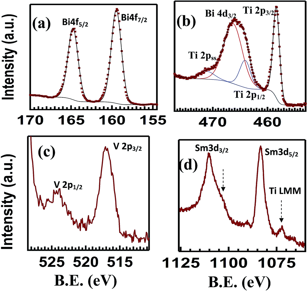 | ||
| Fig. 9 XPS of SBVT sample: (a) Ti 2p, (b) Bi 4f, (c) Sm 3d and (d) V 2p core-levels. | ||
| Ti 2p3/2 | Bi 4f7/2 | Sm 3d5/2 | V 2p3/2 | O 1s | |
|---|---|---|---|---|---|
| BE (eV) | 458.4 | 159.5 | 1083.3 | 516.9 | 530.1 |
| FWHM (eV) | 1.4 | 1.46 | 3.9 | 2.2 | 1.6 |
In order to observe piezo-response (PR) at the granular scale and observe domain switching of SBVT, we performed PFM measurements. The PR was measured from the mirror polished surface of the sample after thermal etching. Fig. 10(a) shows the topographic image of SBVT which is dominated by parallel grooves resulting from the polishing process. The out-of-plane PR amplitude and phase scans, depicted in Fig. 10(b) and (c) respectively, clearly show domains near 5 µm size, attesting genuine PR contrast without any relevant cross talk to topography which has regular grooves and very low rugosity averaging ∼1 nm, although it is possible that domain size and walls could be delimited by grain boundaries. Fig. 10(d) and (e) represent the PR amplitude and phase scans respectively, after bias lithography local poling experiments with ±30Vdc (as outlined in Fig. 10(a)). The PR amplitude contrast presented in Fig. 10(d) reveals a significant imprint and domain reversal features with no visible surface damage, although the PR phase visible in Fig. 10(e) does not present such a strong response. The poor piezoresponse in phase in these experiments can be due to the low dielectric constant between the tip and sample surface as observed in our previous work on piezoelectric ceramics.52 Local piezoresponse hysteresis loop measured by applying a dc voltage of ±40 V between PFM tip fixed above the surface and bottom electrode of the sample is shown in Fig. 10(f). The observation of clear hysteresis suggests the switchable piezoresponse at the nanoscale. Clear hysteresis loops observed for different grain positions indicate that there is no significant effect of grain orientation on local polar character. These studies attest the domain switching and ferroelectric character of SBVT ceramic at the nanoscale.
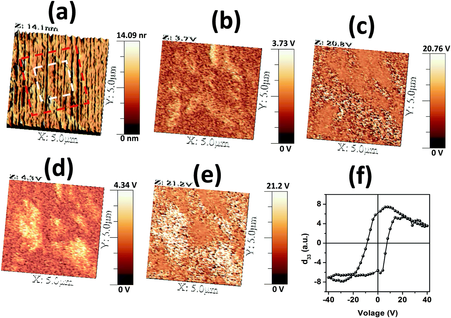 | ||
| Fig. 10 Local PFM images of SBVT. (a) Topography, (b and d) amplitude piezoresponse before and after local poling, (c and e) phase piezoresponse before and after poling. (f) Piezoresponse hysteresis loop. | ||
Fig. 11 shows the UV-Vis diffuse reflectance spectra measured on SBVT powders. The electronic transition in the Aurivillius Bi4Ti3O12 phase is assumed to be indirect allowed,57 thus the apparent optical Eg was calculated via the Tauc formalism, that is a plot of (αhν)1/γ as a function of the photon energy (hν).58,59 The coefficient α can be derived by the Kubelka–Munk theory:60 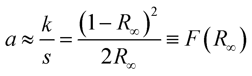 where k and s are the absorption and scattering coefficients, α is the pseudo-absorption coefficient. As SBVT is an indirect semiconductor material, the coefficient γ is equal to 2, thus, the apparent optical Eg of the semiconductor material was obtained from the x-axis (α = 0) intercept of the line which is tangent to the inflection point of the (αhν)1/2 vs. hν curve. This was found by fitting the transformed Kubelka–Munk equation against the photon energy with a sigmoidal Boltzmann function. The apparent optical Eg value was afterward obtained from the x-axis intercept of the line tangent to the inflection point of that curve. SBVT spectrum consists of two distinct absorption edges, the first one, at around 400 nm, the other at approximately 600 nm, as shown in the inset of the figure. The absorption edge located at higher energy, corresponding to an apparent Eg of 2.88 eV (431 nm), noted here as E1g, is consistent with the Eg for Bi4Ti3O12 found by Liu et al.21 On the other hand, the Eg found at lower energy, noted here as E2g, and estimated to be equal to 2.02 eV (613 nm), can be due to contributions of samarium and/or vanadium from the valence band states (hybrid orbitals of Bi 6s and O 2p) to the conduction band states of Ti 3d.61 A conceivable scheme depicting the electrochemical band edges of SBVT – relative to the normal hydrogen electrode (NHE) at pH = 0 – can be drawn. The band edge positions of the conduction band (CB) minimum, as well as of the valence band (VB) maximum of a semiconductor material, can be evaluated knowing the absolute electronegativity values of the constituent atoms of the material:62,63
  and EVB = Eg + ECB. Here Eg is the band gap of the semiconductor material, that was already determined via optical spectroscopy, E0 is a scale factor, equal to −4.5 eV for the NHE, χAaBbCc is the absolute electro-negativity of compound AaBbCc which can be calculated by the formula:63
  where χA is the Pearson's absolute electronegativity of element A. From these calculations, we obtained that the VB maximum of our SBVT is located at 2.87 eV, and consequently, we can represent the band structure of SBVT, together with the inter-band transitions due to Sm and V, in Scheme 1.
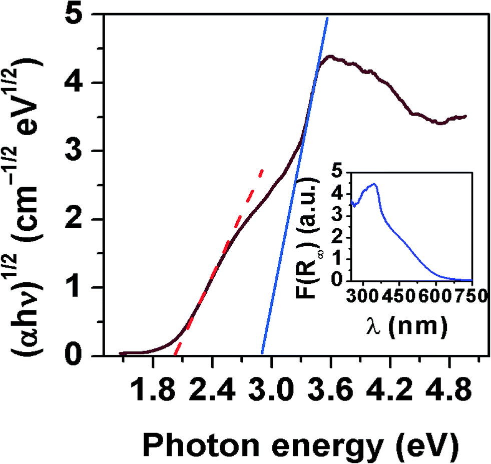 | ||
| Fig. 11 Kubelka–Munk elaboration versus photon energy according to the indirect Eg model (γ = 2). The blue line and the dashed red line represent the x-axis intercept of the line that is tangent to the inflection points of the curve (i.e. apparent optical indirect Egs as calculated using the Tauc procedure). In the inset is reported the DRS spectrum of SBVT. | ||
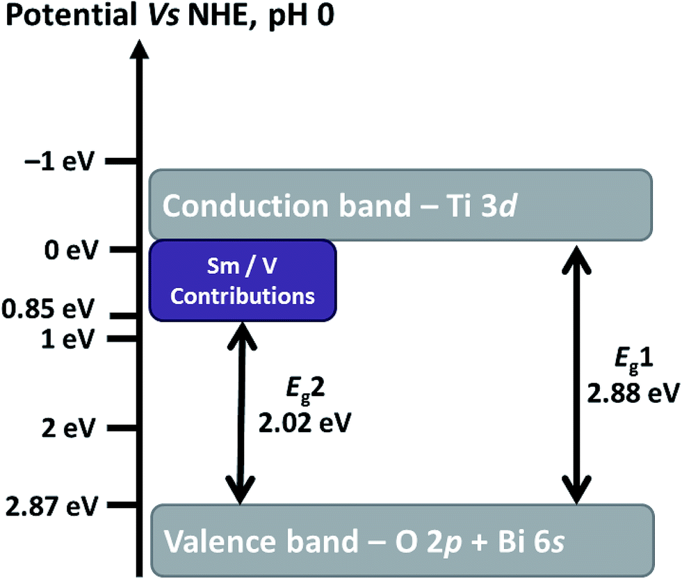 | ||
| Scheme 1 Band structure of SBVT, relative to NHE at pH 0. The inter-band transitions, due to Sm and V, are also reported. | ||
From these findings, the synthesized SBVT, absorbing indeed visible-light, can be used as a visible-light driven photocatalyst.
PCA results in the gas–solid phase are shown in Fig. 12(a) and (c). In dark conditions, there is no degradation of the pollutant gases. After the equilibrium into the reacting system was reached, and the PC reaction was enabled to start, we observe a clear decrease in the NOx concentration. After 60 min irradiation time, the SBVT specimen degraded 12% of the starting NOx amount. The mild PCA of SBVT specimen might be mainly due to its low SSA, that was estimated to be 1.2 ± 0.1 m2 g−1. Also, from the sorption isotherms, Fig. 12(d), we know that the material is a mesoporous material, being the isotherm of type IV, and the presence of no micropores was detected (t-plot, inset of Fig. 12(d)).
 | ||
| Fig. 12 (a) Photocatalytic NOx abatement of SBVT, up to 60 min solar-light irradiation time. Inset: photocatalytic NOx abatement of SBVT, up to 160 min solar-light irradiation time. (b) PCA results of SBVT repeated five consecutive times, shown as a plot of ln(C0/C) as a function of the irradiation time (t). (c) XRD patterns of SBVT before and after five consecutive photocatalytic NOx abatement cycles. (d) Sorption isotherms of SBVT, of type IV. Inset: pore-size distribution. Here VP corresponds to pore volume. | ||
To check the stability and reusability of the sample, PC tests were repeated using the same specimen and protocol as in the first test. Results (for the first 20 min of reaction), are shown in Fig. 12(b) and Table 5. In these, PCA results are given as the apparent pseudo-first order rate constant, k′app. This was done because it is now well established that PC degradation rate obeys Langmuir–Hinshelwood kinetics:64 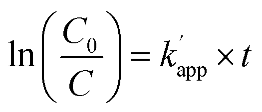 , where C0 is the initial NOx concentration, C is the NOx concentration at time t, and k′app is the apparent pseudo-first-order rate constant. The linear plot between ln(C0/C) and irradiation time (t) reveals the PC reaction to follow pseudo-first order kinetics.
| 1st | 2nd | 3rd | 4th | 5th | |||||
|---|---|---|---|---|---|---|---|---|---|
| k20 × 103 (min−1) | R2 | k20 × 103 (min−1) | R2 | k20 × 103 (min−1) | R2 | k20 × 103 (min−1) | R2 | k20 × 103 (min−1) | R2 |
| 2.4 ± 0.1 | 0.997 | 2.3 ± 0.1 | 0.998 | 2.2 ± 0.1 | 0.999 | 2.3 ± 0.1 | 0.999 | 2.2 ± 0.1 | 0.998 |
As depicted in Fig. 12 and Table 5, SBVT showed itself to be a very stable and reusable photocatalyst. A further proof of the stability of the SBVT as photocatalyst is given by their XRD patterns, recorded before and after five consecutive photocatalytic runs. As it is shown in Fig. 12(c), SBVT did not display any impurity due to decomposition, nor phase separation, this clearly reveals that neither photo-corrosion, nor photo-leaching happened during NOx degradation; furthermore, the specimen also kept its crystallinity after five photocatalytic tests. This confirms the stability and durability of the catalyst under those experimental conditions.
As Dong et al.,65,66 based on electron spin resonance (ESR), have identified O2˙− being the main active reactive oxygen species (ROS) responsible for the reduction of NO, a mechanistic insight of the NOx photodegradation can be proposed as follows, when visible-light reaches the surface of SBVT specimen:
| SBVT + hν → eCB− + hVB+ | (1) |
| eCB− + O2 → O2˙− | (2) |
| NO + O2˙− → NO3− | (3) |
| NO3− + H+ → HNO3 | (4) |
On the other hand, photo-generated holes might also react with water molecules adsorbed on the surface of SBVT, giving:
| hVB+ + H2O(ads) → OH˙ + H+ | (5) |
| hVB+ + OH− → OH˙ | (6) |
| NO + OH˙ → NO2 + H+ | (7) |
| NO2 + OH˙ → NO3− + H+ → HNO3 | (8) |
As shown in eqn (4) and (8), the final product of NOx degradation is nitric acid. HNO3 produced on the surface of the photocatalyst might actually act as a physical barrier, and might inhibit the PC reaction67 – this also explains why the repeated PCA tests were carried out for up to 20 min solar-light irradiation time.54 For this reason, a further PC test was assessed until 160 min irradiation time, till the reaching of a plateau. This is reported in Fig. 12(a), where it can be seen that the NOx degradation stops at ∼120 min irradiation time, reaching a maximum degradation of ∼17%. In any case, it has to be stressed that the formed HNO3 can be easily eluted from the photocatalyst into water.68
4. Conclusions
We studied temperature variation of structural properties of Sm and V co-doped BTO ceramics by means of in situ XRD and Raman spectra. We found that SBVT ceramics have an orthorhombic structure with large structural distortions compared to pure and other rare-earth doped BTO ceramics which was attributed to the difference in ionic radius. With the increase in temperature a systematic increase in lattice parameters with an anomaly around the ferroelectric–paraelectric transition temperature was observed. A strong decrease in orthorhombicity and growth of tetragonal peaks in the vicinity of TC were seen. From the thermal evaluation of Raman modes of several A- and B-site modes we found that the bending Bi atomic vibrations of perovskite slabs experience the phase transition earlier compared to torsional bending of BO6 octahedra. From the ferroelectric and piezoelectric studies, it was confirmed that SBVT presents strong ferroelectric domain switching properties compared to other rare-earth doped BTO ceramics, making it a suitable material for memory applications with resistance to polarization fatigue up to 108 switching cycles. SBVT possesses a lower energy bandgap of 2 eV compared to its parent compound which can be a candidate for photovoltaic applications as the PV conversion efficiency is reported to be improved for smaller bandgap ferroelectrics. By means of gas phase-solid photocatalysis test we observed that the sample exhibited a mild, yet reproducible PC activity, being the photocatalyst stable and recyclable. The low PC activity in this study was due to the lower specific surface area and the results can be improved when prepared in nano scale.Note added after first publication
This article replaces the version published on 1st February 2017, in which an incorrect version of Fig. 1 was presented through editorial error.Acknowledgements
The authors would like to acknowledge the financial support from FCT, Portugal (SFRH/BPD/75582/2010) and COMPETE 2020, financed by national funds of FCT under the project UID/CTM/50025/2013. This work was developed in the scope of the project CICECO – Aveiro Institute of Materials (ref. FCT UID/CTM/50011/2013), financed by national funds through the FCT/MEC and when applicable co-financed by FEDER under the PT2020 partnership agreement. MJH acknowledges UID/EMS/00481/2013 project. MKS acknowledges Bilateral Indo-Portuguese 2015/2017 Project and FCT 2013 Investigator Call (IF/00976/2013).References
- B. H. Park, B. S. Kang, S. D. Bu, T. W. Noh, J. Lee and W. Jo, Nature, 1999, 401, 682–684 CrossRef CAS.
- U. Chon, H. M. Jang, M. G. Kim and C. H. Chang, Phys. Rev. Lett., 2002, 89, 087601 CrossRef PubMed.
- L. B. Kong, T. S. Zhang, J. Ma and F. Boey, Prog. Mater. Sci., 2008, 53, 207–322 CrossRef CAS.
- H. Yan, H. Zhang, R. Ubic, M. J. Reece, J. Liu, Z. Shen and Z. Zhang, Adv. Mater., 2005, 17, 1261–1265 CrossRef CAS.
- R. E. Newnham, R. W. Wolfe and J. F. Dorrian, Mater. Res. Bull., 1971, 6, 1029–1039 CrossRef CAS.
- V. A. Isupov, Ferroelectrics, 1996, 189, 211–227 CrossRef CAS.
- Y. Noguchi and M. Miyayama, Appl. Phys. Lett., 2001, 78, 1903–1905 CrossRef CAS.
- S. S. Kim, T. K. Song, J. K. Kim and J. Kim, J. Appl. Phys., 2002, 92, 2213–2215 CrossRef CAS.
- C. Zhang and Y. Zhu, Chem. Mater., 2005, 17, 3537–3545 CrossRef CAS.
- A. Kudo, K. Omori and H. Kato, J. Am. Chem. Soc., 1999, 121, 11459–11467 CrossRef CAS.
- M. Oshikiri, M. Boero, J. Ye, Z. Zou and G. Kido, J. Chem. Phys., 2002, 117, 7313–7318 CrossRef CAS.
- Y. G. Zhang, H. W. Zheng, J. X. Zhang, G. L. Yuan, W. X. Gao, Y. Z. Gu, C. L. Diao, Y. F. Liu and W. F. Zhang, Mater. Lett., 2014, 125, 25–27 CrossRef CAS.
- F. Yakuphanoglu, A. Tataroğlu, A. A. Al-Ghamdi, R. K. Gupta, Y. Al-Turki, Z. Şerbetçi, S. B. Omran and F. El-Tantawy, Sol. Energy Mater. Sol. Cells, 2015, 133, 69–75 CrossRef CAS.
- H. He, Z. He, Z. Jiang, J. Wang, T. Liu and N. Wang, J. Alloys Compd., 2017, 694, 998–1003 CrossRef CAS.
- Z. Chen, H. Jiang, W. Jin and C. Shi, Appl. Catal., B, 2016, 180, 698–706 CrossRef CAS.
- T. Cao, Y. Li, C. Wang, Z. Zhang, M. Zhang, C. Shao and Y. Liu, J. Mater. Chem., 2011, 21, 6922–6927 RSC.
- D. Hou, X. Hu, P. Hu, W. Zhang, M. Zhang and Y. Huang, Nanoscale, 2013, 5, 9764–9772 RSC.
- Z. Dai, F. Qin, H. Zhao, J. Ding, Y. Liu and R. Chen, ACS Catal., 2016, 6, 3180–3192 CrossRef CAS.
- H. Shi, H. Tan, W.-b. Zhu, Z. Sun, Y. Ma and E. Wang, J. Mater. Chem. A, 2015, 3, 6586–6591 CAS.
- W. Zhao, Z. Jia, E. Lei, L. Wang, Z. Li and Y. Dai, J. Phys. Chem. Solids, 2013, 74, 1604–1607 CrossRef CAS.
- Y. Liu, M. Zhang, L. Li and X. Zhang, Appl. Catal., B, 2014, 160–161, 757–766 CrossRef CAS.
- X. Li, Z. Zhu, F. Li, Y. Huang, X. Hu, H. Huang, R. Peng, X. Zhai, Z. Fu and Y. Lu, Sci. Rep., 2015, 5, 15511 CrossRef CAS PubMed.
- A. H. Mamaghani, F. Haghighat and C.-S. Lee, Appl. Catal., B, 2017, 203, 247–269 CrossRef CAS.
- N. Imanaka and T. Masui, Appl. Catal., A, 2012, 431–432, 1–8 CrossRef CAS.
- World Health Organization, WHO guidelines for indoor air quality: selected pollutants, WHO Regional Office for Europe, Denmark, 2010 Search PubMed.
- A. C. Larson and R. B. Von Dreele, General structure analysis system (GSAS), National Laboratory Report LAUR, Los Alamos, 2004 Search PubMed.
- B. H. Toby, J. Appl. Crystallogr., 2001, 34, 210 CrossRef CAS.
- O. Hertel and M. Evan Goodsite, in Air Quality in Urban Environments, The Royal Society of Chemistry, 2009, vol. 28, pp. 1–22 Search PubMed.
- D. M. Tobaldi, R. C. Pullar, R. Binions, A. Belen Jorge, P. F. McMillan, M. Saeli, M. P. Seabra and J. A. Labrincha, Catal. Sci. Technol., 2014, 4, 2134–2146 CAS.
- D. M. Tobaldi, R. C. Pullar, L. Duraes, T. Matias, M. P. Seabra and J. A. Labrincha, CrystEngComm, 2016, 18, 164–176 RSC.
- F. L. Toma, G. Bertrand, D. Klein and C. Coddet, Environ. Chem. Lett., 2004, 2, 117–121 CrossRef CAS.
- C. H. Hervoches and P. Lightfoot, Chem. Mater., 1999, 11, 3359–3364 CrossRef CAS.
- W. Dollase, J. Appl. Crystallogr., 1986, 19, 267–272 CrossRef CAS.
- K. Momma and F. Izumi, J. Appl. Crystallogr., 2008, 41, 653–658 CrossRef CAS.
- W. H. Baur, Acta Crystallogr., Sect. B: Struct. Crystallogr. Cryst. Chem., 1974, 30, 1195–1215 CrossRef CAS.
- K. Robinson, G. V. Gibbs and P. H. Ribbe, Science, 1971, 172, 567–570 CAS.
- H. Du, S. Wohlrab and S. Kaskel, J. Phys. Chem. C, 2007, 111, 11095–11103 CAS.
- E. Venkata Ramana, M. P. F. Graça, M. A. Valente and T. Bhima Sankaram, J. Alloys Compd., 2014, 583, 198–205 CrossRef CAS.
- T. Hirata and T. Yokokawa, Solid State Commun., 1997, 104, 673–677 CrossRef CAS.
- P. R. Graves, G. Hua, S. Myhra and J. G. Thompson, J. Solid State Chem., 1995, 114, 112–122 CrossRef CAS.
- Y. H. Wang, C. P. Huang and Y. Y. Zhu, Solid State Commun., 2006, 138, 229–233 CrossRef CAS.
- J. Min Ku, K. Yong-Il, S. Jung Min and W. Seong Ihl, J. Phys. D: Appl. Phys., 2004, 37, 2588 CrossRef.
- K. Liang, Y. Qi and C. Lu, J. Raman Spectrosc., 2009, 40, 2088–2091 CrossRef CAS.
- M. K. Jeon, Y.-I. Kim, S.-H. Nahm and S.-I. Woo, J. Korean Phys. Soc., 2004, 45, 1240–1243 CAS.
- S. Kojima and S. Shimada, Phys. B, 1996, 219, 617–619 CrossRef.
- C. H. Hervoches, A. Snedden, R. Riggs, S. H. Kilcoyne, P. Manuel and P. Lightfoot, J. Solid State Chem., 2002, 166, 449 CrossRef CAS.
- J. Hou, S. Jiao, H. Zhu and R. V. Kumar, CrystEngComm, 2011, 13, 4735–4740 RSC.
- H. Qi, Y. Qi and M. Xiao, J. Mater. Sci.: Mater. Electron., 2014, 25, 1325–1330 CrossRef CAS.
- H. Du, L. Tang and S. Kaskel, J. Phys. Chem. C, 2009, 113, 1329–1339 CAS.
- C. W. Ahn, H. J. Lee, I. W. Kim, J. S. Lee and W. K. Lee, Ferroelectrics, 2006, 331, 129–134 CrossRef CAS.
- C. Q. Huang, M. Chen, R. F. Liu, X. A. Mei and J. Liu, Key Eng. Mater., 2012, 512–515, 1333–1336 CrossRef CAS.
- G. Viola, K. Boon Chong, M. Eriksson, Z. Shen, J. Zeng, Q. Yin, Y. Kan, P. Wang, H. Ning, H. Zhang, M. E. Fitzpatrick, M. J. Reece and H. Yan, Appl. Phys. Lett., 2013, 103, 182903 CrossRef.
- E. Venkata Ramana, F. Figueiras, A. Mahajan, D. M. Tobaldi, B. F. O. Costa, M. P. F. Graca and M. A. Valente, J. Mater. Chem. C, 2016, 4, 1066–1079 RSC.
- D. M. Tobaldi, M. P. Seabra, G. Otero-Irurueta, Y. R. de Miguel, R. J. Ball, M. K. Singh, R. C. Pullar and J. A. Labrincha, RSC Adv., 2015, 5, 102911–102918 RSC.
- F. E. Oropeza, I. J. Villar-Garcia, R. G. Palgrave and D. J. Payne, J. Mater. Chem. A, 2014, 2, 18241–18245 CAS.
- C. Suzuki, J. Kawai, M. Takahashi, A.-M. Vlaicu, H. Adachi and T. Mukoyama, Chem. Phys., 2000, 253, 27–40 CrossRef CAS.
- H. Gu, D. Bao, S. Wang, D. Gao, A. Kuang and X. Li, Thin Solid Films, 1996, 283, 81–83 CrossRef CAS.
- J. Tauc, R. Grigorovici and A. Vancu, Phys. Status Solidi B, 1966, 15, 627–637 CrossRef CAS.
- K. A. Michalow, D. Logvinovich, A. Weidenkaff, M. Amberg, G. Fortunato, A. Heel, T. Graule and M. Rekas, Catal. Today, 2009, 144, 7–12 CrossRef CAS.
- A. S. Marfunin, Physics of minerals and inorganic materials : an introduction, ed. A. S. Marfunin, N. G. Egorova and A. G. Mishchenko, Springer-Verlag, Berlin, New York, 1979 Search PubMed.
- W. Wei, Y. Dai and B. Huang, J. Phys. Chem. C, 2009, 113, 5658–5663 CAS.
- R. G. Pearson, Inorg. Chem., 1988, 27, 734–740 CrossRef CAS.
- Y. Xu and M. A. A. Schoonen, Am. Mineral., 2000, 85, 543–556 CrossRef CAS.
- Y. Paz, in Photocatalysis: fundamentals and perspectives, The Royal Society of Chemistry, 2016, pp. 80–109, 10.1039/9781782622338-00080.
- F. Dong, Z. Zhao, Y. Sun, Y. Zhang, S. Yan and Z. Wu, Environ. Sci. Technol., 2015, 49, 12432–12440 CrossRef CAS PubMed.
- F. Dong, Z. Wang, Y. Li, W.-K. Ho and S. C. Lee, Environ. Sci. Technol., 2014, 48, 10345–10353 CrossRef CAS PubMed.
- Y. Ohko, Y. Nakamura, A. Fukuda, S. Matsuzawa and K. Takeuchi, J. Phys. Chem. C, 2008, 112, 10502–10508 CAS.
- T. Ibusuki and K. Takeuchi, J. Mol. Catal., 1994, 88, 93–102 CrossRef CAS.
Footnote |
| † Electronic supplementary information (ESI) available. See DOI: 10.1039/c7ra00021a |
| This journal is © The Royal Society of Chemistry 2017 |