
 Open Access Article
 This Open Access Article is licensed under a
 Creative Commons Attribution 3.0 Unported Licence
Current status of electron transport layers in perovskite solar cells: materials and properties
Khalid
Mahmood
 *a,
Saad
Sarwar
b and
Muhammad Taqi
Mehran
b
*a,
Saad
Sarwar
b and
Muhammad Taqi
Mehran
b
aDepartment of Chemical & Polymer Engineering, University of Engineering & Technology Lahore, Faisalabad Campus, 3½ Km. Khurrianwala – Makkuana By-Pass, Faisalabad, Pakistan. E-mail: khalid@kaist.ac.kr
bUniversity of Science and Technology (UST), 217-Gajeong-ro, Yuseong-gu, Daejeon, 34113, Republic of Korea
First published on 17th March 2017
Abstract
Methyl ammonium lead halide-based hybrid perovskite solar cells (PSCs) have been intensively studied in recent years because of their high efficiency and low processing costs. Although there are limited constraints for choosing the planar electron transport layer (ETL) or mesoscale electron transporting material (ETM), a great deal of effort is required in designing complex nanostructures which are effective as ETL/ETM to achieve high open circuit voltage (Voc) and high fill factor (FF) in PSCs. In this review, various inorganic and organic ETLs, as well as inorganic ETM systems, used for PSCs are summarized. The transport mechanism of electrons in these different ETL/ETM materials is discussed along with their effect on Voc on the basis of energy band diagrams with respect to the perovskite absorber. The authors also discuss the microstructure/nanostructure aspect of mesoscopic ETMs, doping and surface functionalization, and the influence of these parameters on solar cell behaviour, performance, and hysteresis effects. The authors also discussed the microstructure/nanostructure aspect of ETL on shape of current density vs. voltage (J–V) hysteresis in this review. Technical issues and recent progress of ETL to improve device efficiency and stability in terms of materials, process, and characterization are summarized.
1. Introduction
The hybrid nature (inorganic and organic) of perovskite materials1 facilitates their use in devices such as solar cells,2 light emitting diodes,3,4 photodetectors,5–8 ferroelectric devices, and ferromagnetic devices.9 A hybrid perovskite (RMX3 where R: alkyl, A: ammonium, M: metal and X: halogen) solar cell has the potential to offer low-cost solar energy conversion and can be fabricated on glass and flexible substrates.10–18 In particular, methyl (M) ammonium (NH3+) metal (Sn, Pb and Eu) halide (Cl, Br and I) is suitable for solar cells because of its optimum band gap (1.3–2.9 eV),8–12 and its band gap can be tuned with different metal ions and halide cations, as well as different metal doping to its backbone.19–22 For example, use of formamidinium (FA) rather than methyl ammonium lowers the band gap; with the absorption band tail eventually exceeding 800 nm.23,24 This versatile material also has a higher exciton diffusion length (1000 nm) and lower exciton binding energy with broad spectral absorption and visible emission providing more room for device researchers to explore the physics behind the perovskite solar cell (PSC).25–29 A hybrid PSC can achieve efficiency as high as 20% within a short period of time.30 This peculiar material has triggered extensive study into material and fundamental physics for next generation solar cell materials because of the variety of fabrication techniques and exceptional optoelectronic properties. It is hoped that the efficiency will exceed that of crystalline silicon solar cells in the near future. Effective masses of photogenerated electrons and holes have been estimated as me* = 0.23m0 and mh* = 0.29m0, respectively, including spin–orbit coupling effects.20,31,32 Theoretical studies have explained the ambipolar characteristics of electrons and holes with efficient transport properties.To date, several electron transport layers (ETLs) have been reported, including metal oxides (mainly transition metal oxides), metal oxide composites, and metal oxide heterostructure nanoparticles.
The crystal structure of hybrid perovskite materials and hybrid PSCs is well known, and the crystal structure analysis has been discussed thoroughly by different groups.1 There have been more than 500 articles published within a 5 year span with different device geometry from the concept of dye sensitized solar cells (DSSC)2 to p–n/p–i–n geometry,33 bulk hetero-junction solar cells,34–36 and inverted planar structure.37–40 Efficiency increased in order from the initial PSC invented by Miyasaka's group.2 Later work by different groups improved the efficiency by using different materials from the bottom to the top electrode. This was found to be the easiest way to improve the power conversion efficiency (PCE) by increasing the open circuit voltage (Voc) and short circuit current (Jsc) in the early stages of device research.
The ETL, sometimes called the electron extraction layer or electron collection layer, is where electrons are injected from the absorber layer, transported through the electron transporting materials (ETM), and finally collected by the electrode. Sometimes the ETL is replaced by a composite photoelectrode to improve the charge collection efficiency by lowering the series resistance.34–36 Moreover, a one-dimensional nanorod ETL provides fast charge transport in a photovoltaic cell. Excellent pore filling achieved by manipulating the gaps between the nanorods and nanosheets was found to be beneficial for enhancing the fill factor (FF) and PCE.41–52 The gaps between the nanorods can be controlled by the concentration of the solution and seed nanoparticle films. The efficient charge collection leads to ideal current–voltage behaviour. This is a method by which to improve the external quantum efficiency (EQE), giving maximum efficiency without thermalization.
A schematic diagram of device architecture of the PSC is presented in Fig. 1. The simple PSC consists of an electron transport layer/perovskite/hole transport layer on the FTO/glass substrate. Low and high work function electrodes can be used at the ETL and hole transport layer (HTL) sides, respectively. The balanced diffusion length of electron and hole is more than 500 nm in a perovskite absorber, which inhibits charge recombination in the perovskite absorber.25,26 Recently, Dong et al. reported electron–hole diffusion length of more than 175 microns in CH3NH3PbI3.27 Therefore, a smooth electron injection requires after charge separation for further process. Sometimes a compact hole blocking layer is used before the ETL,53,54 and an electron blocking layer55,56 is used before the HTL to block the excess hole and electron at either side, respectively. Some earlier studies focused on compact hole blocking layer (HBL) being beneficial for PCE by blocking the hole from the ETL side.53,54 The electron and hole clouding in the device architecture leads to a high recombination rate. Using a planar hetero junction PSC, the PCE can be significantly improved by provision of a proper path for both electron and hole.
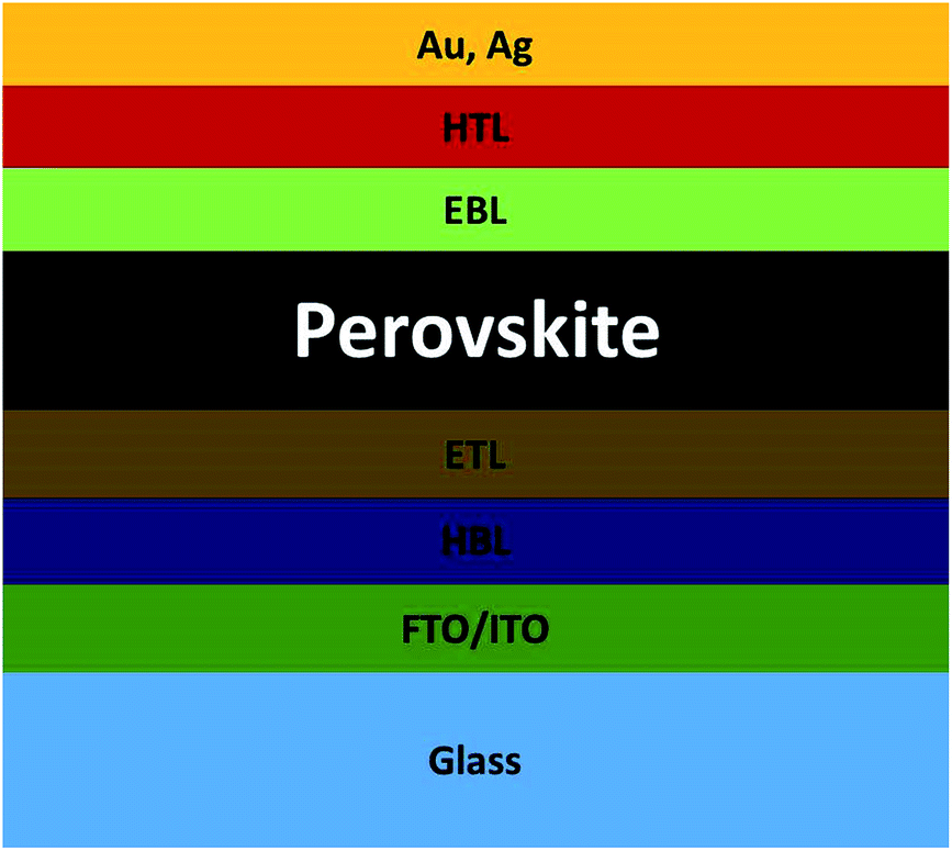 | ||
| Fig. 1 Schematic of perovskite solar cell. | ||
In this review, we discuss the material and electrical aspects of the importance of the ETL along with their device physics. There is evidence that the exciton might dissociate at the ETL/perovskite and perovskite/HTL interfaces. The other factor is exciton diffusion and separation, which is not clearly understood in PSCs. Low exciton energy in perovskite appears to have benefit for high exciton diffusion length, which is an advantage over polymer/organic solar cells. Another important factor is that PSCs fit to inorganic as well as polymer/organic ETL and HTL. Inorganic ETL/HTL has a longer electron/hole diffusion length compared with organic/polymer ETL/HTL. It has been reported that hybrid solar cells do not necessarily need a HTL but do need an ETL/scaffold.57 So choice of the proper ETL for PSC is vital. Several reviews have been reported within a short period of time on PSC research.58–66
In this review, we summarize different ETL used in hybrid PSC and explore how design of ETL helps to improve the overall device performance. We also discuss how to improve solar cell efficiency in terms of improving charge injection, charge collection, charge separation, and charge transport in ETM. These parameters are interlinking to achieve the overall performance. We also address the effect of microstructure and morphology of ETL materials and how to achieve better pore filling, and composite structure to achieve high electron injection and transport on open circuit voltage. Finally, we review the different processing methods of ETL and their advantages and disadvantages. Herein, the most recent results of this particular optimization process such as annealing temperature and annealing time are reviewed, and how certain ETM retard the charge recombination.
2. Characteristics of electron transporting layer
The most important characteristic of an ETL is that it must satisfy band alignment with the perovskite layer, i.e. it should have lowest unoccupied molecular orbital (LUMO) and highest occupied molecular orbital (HOMO) higher than the perovskite active layer. It must have high transmittance in the UV-Vis region so that a photon can pass through easily and be absorbed by the perovskite absorber. Exciton generation via light absorption, across the perovskite layer, must be dissociated before collection either by the ETL or HTL. The exciton dissociation mechanism was explained by Savenije et al.68 Excitons can be dissociated at the ETL/perovskite or perovskite/HTL interfaces. Recently, studies showed that the electron and hole diffusion lengths exceed 500 nm and 1000 nm for CH3NH3PbI3. X-ray diffraction (XRD) and transmission electron microscopy (TEM) analysis of the different groups showed that perovskite films were highly crystalline and defect-free using the one step or two step methods.1–10,18–493. Different ETL materials used in perovskite solar cells
A number of metal oxides, such as TiO2, ZnO, SnO2, SiO2, ZrO2, can either be used as ETL or scaffold material. Each material has specific advantages to boost the PCE. Two types of solution process have been used to fabricate PSC. One-step deposited perovskite led to average PCE of 8.19% from rutile-perovskite solar cells and 7.23% from anatase-perovskite solar cells. Nanova et al. predicted that an optimum porosity and an optimum over layer of perovskite is necessary to control the shunt resistance and series resistance.69 Using chemical bath-deposited rutile thin films and TiCl4 treatment with different concentrations, Yella et al. successfully modified the particle size of rutile TiO2 to give PCE as high as 13.7%.70A complete list of electron, hole injection and exciton annihilation processes is described by Luo et al.66 The large variety of ETL/ETM makes it hard to define the characteristics of the ideal ETL. In terms of considering the band offset between the ETL/perovskite, Minemoto et al. theoretically calculated that the band offset between the ETL/absorber and HTL/absorber should be 0.0–0.3 eV, as shown in Fig. 2.67 Fig. 2 shows simulated J–V curves of PSC with different CBO values for the buffer/absorber interface.
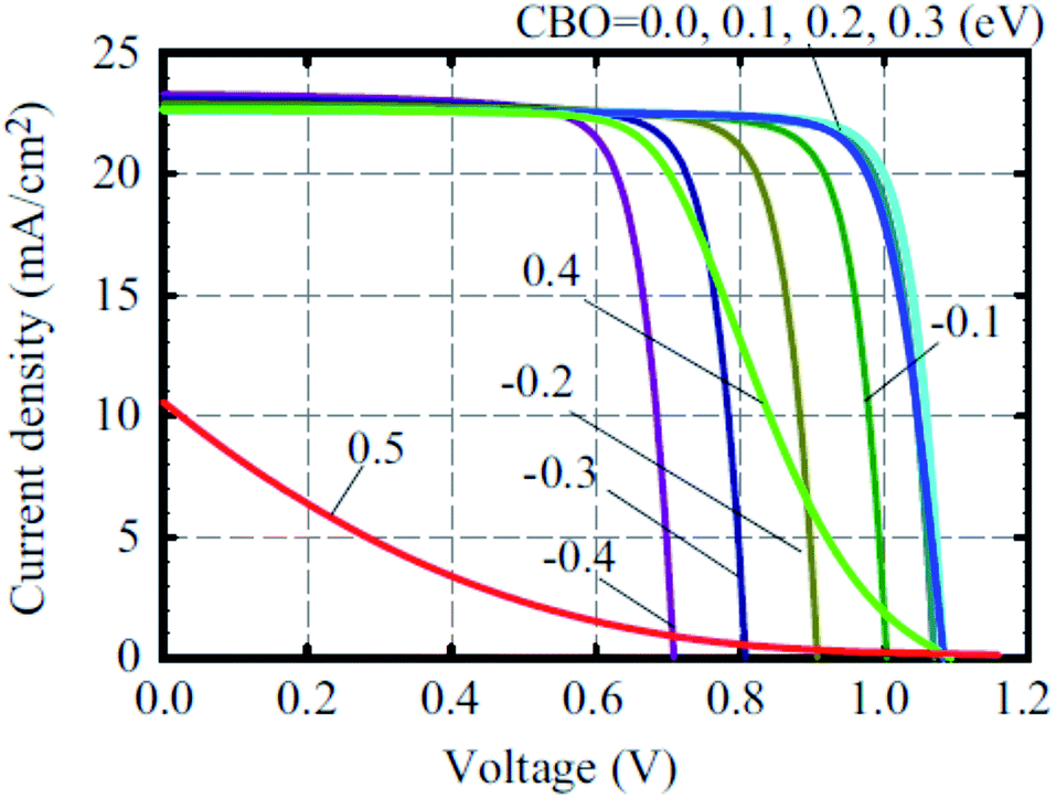 | ||
| Fig. 2 J–V curves of perovskite solar cells with different CBO values of buffer/absorber interface. Here, the VBO of the absorber/HTM interface was set to 0 and the interface defect density of IDL 1 was set to 1016 cm−3.67 | ||
3a. Metal oxide as ETL materials
The PSC was initiated by Miyasaka's group (Tokyo Univ.) in 2009.2 Using two different types of organo-lead halide perovskite nanocrystals, CH3NH3PbBr3 and CH3NH3PbI3, they efficiently sensitized TiO2 for visible-light conversion in photoelectrochemical cells with photovoltage of 0.97 V and PCE limited to 3.8%. Later work by Park's group (Sungkyunkwan Univ.), Snaith's group (Oxford Univ.), and Gratzel's group (Ecole Polytechnic) tremendously advanced research in PSC and achieved efficiency of more than 15%. Initially, the PSC required a glove box to control the atmosphere. Recently, Yang's (UCLA) research group reported 19.3% efficient PSC using a polyethyleneimine (PEI) thin layer on TiO2 as ETM fabricated in air.71 In addition, doped ETM was shown to improve efficiency by tuning the band gap and Fermi level, which can increase/decrease the open circuit voltage. Using n-type doping in transition metal oxide ETM, the Fermi level can be increased, which allows the electron to have a smooth injection from the perovskite active layer. Many groups have also used core–shell nanoparticles Al2O3/ZnO,72 TiO2/MgO,73 and WO3/TiO2 (ref. 74) for charge retardation, and improved charge recombination resistance by insulating material with efficient charge injection and charge transport.To date, TiO2 is the ETL material most widely used by different research groups. But, Snaith et al. pointed out that a TiO2-based PSC had lower stability than a TiO2-free PSC.75 They studied the stability of ss-DSSC and PSC using transient absorption spectroscopy (Fig. 3). Snaith's group initiated the idea that the absorption tails of mesoporous TiO2 extend into the visible region, which may degrade the stability over a longer timescale.76 They suggested that a low cost UV filter could efficiently block the UV and enhance the stability for a longer period of time.
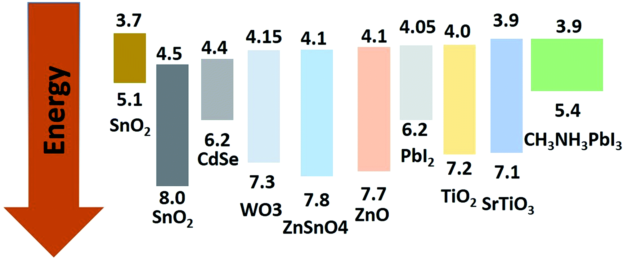 | ||
| Fig. 3 Band energy diagram of different ETL with respect to perovskite. | ||
Ultra-thin amorphous TiOx provides uniformity and homogeneity in short range order, giving more highly stable electronic properties than mesoporous TiO2. A 12.2% efficient PSC with high bending and durability was achieved using 20 nm of atomic layer deposited (ALD) TiOx by Kim et al.18
Cadmium selenide (CdSe) has a band gap of 1.8 eV, with HOMO 0.5 eV lower than the perovskite active layer and LUMO 0.6 eV higher than the perovskite active layer. CdSe nanocrystal used as an electron transport/extraction layer for PSC shows PCE up to 11.7%.78 Strong PL quenching has been observed in CdSe/CH3NH3PbI3/Spiro-OMeTAD. The PL quenching effect is necessary in PV devices for better charge separation and recombination resistance. SnO2 shows better environmental stability than TiO2, as reported by Song et al.79 Using the concept of light scattering efficiency, Park et al. used TiO2 nanohelix ETL deposited by oblique-angle e-beam evaporation to produce hysteresis-free PSC.80 The drawback of using TiO2 in PSCs is that it must be annealed at high temperature, which can be a hindrance in commercialization as well as use in flexible devices as the substrate cannot withstand such high temperatures. While mesoporous TiO2 incorporated PSCs have shown good efficiency, their counterpart, the planar type PSC typically suffers from hysteresis issues. Recently several groups have addressed this issue by replacing the TiO2 with low temperature processed SnO2 in planar structures. SnO2 has advantages over TiO2 in terms of its high electron mobility, anti-reflection property, and deeper conduction band, which could increase charge transfer from perovskite to ETL and reduce charge accumulation at the interface. Weijun Ke et al. deposited SnO2 by spin-coating precursor solutions of SnCl2·H2O and heating in the air at 180 °C.147 A high efficiency of 17.21% was achieved using this method. Although less than in the planar TiO2 structure, hysteresis was still present in PSCs made using this method. Qi Jiang et al. obtained a certified high efficiency of 19.9% by employing solution-processed SnO2 at a low temperature of 150 °C, which was almost free of hysteresis.148 However, passivation of the PbI2 phase in the perovskite layer was introduced in this study, which might have played a role in such a high efficiency of the device. Researchers have also employed atomic layer deposited (ALD) SnO2 in a PSC, which served as the top cell in a tandem device. An efficiency of 20% was obtained with this configuration. However, as ADL is not cost-effective commercially, the researchers employed a combination of spin-coating and chemical bath deposition of SnO2 to form the ETL.149 Devices made using this method showed better performance than devices made by ALD, mainly because of an improved FF. The higher roughness of the SnO2 achieved from the new technique results in better contact of the ETL and perovskite layer, thus increasing the FF. The devices showed a mild hysteresis, although much better than that of the planar TiO2 devices, and showed a highest efficiency of 21% (planar structure). The devices retained 82% of efficiency after ageing for 60 h under illumination of 100 mW cm−2. This is similar to the ageing behaviour of high temperature mesoporous films. A steady-state efficiency of 17.54% was also obtained using an effective interface engineering technique for planar PSCs employing SnO2 as an electron selective layer.150
3b. Scaffold material for perovskite solar cells
Unusually high efficiency was reported using SiO2, Al2O3, and ZrO2 as scaffold material in PSC. A PCE of up to ∼10% was reported by different research groups using SiO2,81 Al2O3,82,83 and ZrO2 (ref. 84) as scaffold material. A material with lower conduction band edge, and higher valence band edge can effectively inject electron and block hole from the perovskite layer, which can improve the recombination resistance for a highly efficient PSC. For SiO2, Al2O3, and ZrO2, the band gap is larger, and the conduction band edge is much higher than the conduction band of the perovskite layer which prevents smooth electron injection into both SiO2 and ZrO2. Thus, the excited electron remains in the conduction band of the perovskite layer for a longer time. It was also proposed that the perovskite layer exhibits an ambipolar nature and that the electron can remain in the conduction band with only hole transported to the HTL. Bi et al. reported ZrO2 as a scaffold material and compared the PCE with TiO2 ETL.84 Their results showed that ZrO2 (PCE: 10.8%) had higher efficiency than TiO2 (PCE: 9.8%). Although the band alignment is not fulfilled when ZrO2 is used as scaffold material, the higher photovoltage and higher electron lifetime make ZrO2 an efficient scaffold material, as shown in Fig. 4. Al2O3 acts as an excellent protective material for degradation of PSC. As can be seen in Fig. 5, a comparative study by Niu et al.82 showed that Al2O3 retained the optical absorbance of perovskite and maintained the stability of the PSC by extracting moisture from the perovskite layer (Fig. 7).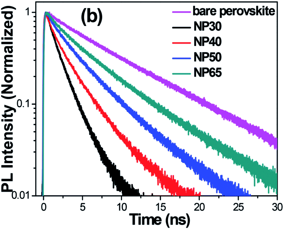 | ||
| Fig. 4 TR-PL decays of bare CH3NH3PbI3 deposited on Pyrex glass and the FTO/TiO2/CH3NH3PbI3 devices employing NP30, NP40, NP50, and NP65. It can be seen clearly that the TR-PL decay is accelerated with decrease in the size of TiO2 NPs. The time resolution of the TR-PL measurement was ∼190 ps.77 | ||
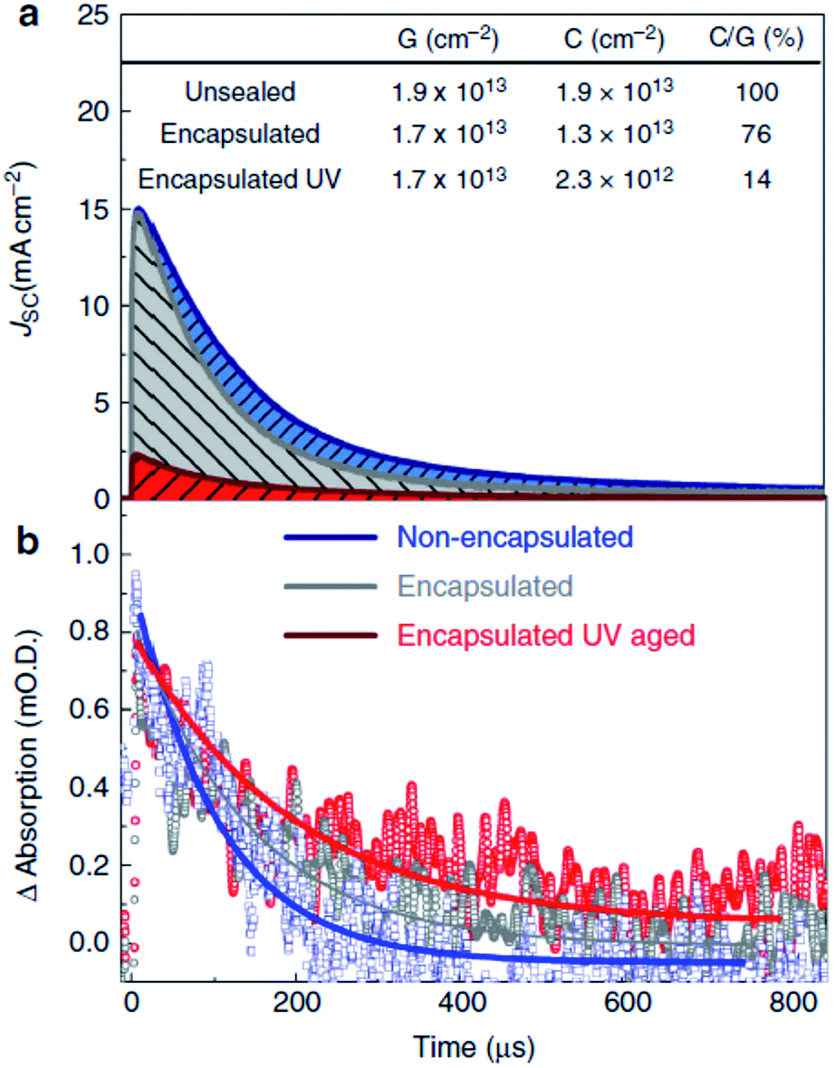 | ||
| Fig. 5 Current extraction and transient absorption spectroscopy of TiO2-based solar cells. In the top panel (a), the current collected from full perovskite-sensitized TiO2 solar cells with semi-transparent electrodes (15 nm gold) after a 10 ns laser pulse (550 nm) is plotted against time after the excitation. Non-encapsulated (blue), encapsulated after ambient light exposure (grey), and encapsulated after UV aging (red) (5 min at 40 mW cm−2, 365 nm) are compared. The area underneath the curves represents the total amount of collected charge. In the bottom panel (b), the transient absorption trace at short circuit of the hole on Spiro-OMeTAD is probed at 510 nm, performed simultaneously with the current extraction. The lines are merely guides to the eye. The table in the figure shows the charge generated (G, estimated from the early time transient absorption signal), collected (C, by integrating the current decay), and the ratio between the two as a percentage (C/G). The laser intensity was 80 mJ cm−2, giving charge densities similar to those found in devices under operating conditions.75 | ||
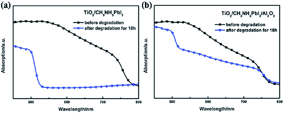 | ||
| Fig. 6 UV-Vis spectra of sensitized films. (a) Film of TiO2/CH3NH3PbI3 before and after degradation, (b) Film of TiO2/CH3NH3PbI3/Al2O3 before and after degradation. The degradation time is 18 h.83 | ||
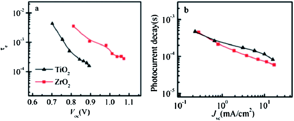 | ||
| Fig. 7 (a) Electron lifetime as a function of open circuit voltage in Spiro-OMeTAD/CH3NH3PbI3/ZrO2 (or TiO2) solar cells. (b)84 Photocurrent transient decay occurs as a function of short-circuit current in Spiro-OMeTAD/CH3NH3PbI3/ZrO2 (or TiO2) solar cells.84 | ||
Using an ultra-thin Al2O3 layer, excellent moisture and humidity stability was demonstrated by Dong et al.83 Using computational analysis along with experimental results, they proved that thin layer Al2O3 acts an excellent absorber of H2O from the perovskite layer.
3c. Organic ETL materials
Metal oxide-free PSC have been prepared using organic semiconductors. Many groups have reported organic ETL such as PEHT, PCBM, PEHT:PCBM85–95 composites to achieve high efficiency in inverted PSC. Using an organic or polymer material with metal oxide scaffold/electron blocking layer, PSC can be prepared with improved efficiency. Many polymers satisfy the condition mentioned in the above section that the LUMO must be lower than that of the perovskite layer. A NiO2 electron blocking layer and HTL with PCBM/BCP as an ETL was reported by Wang et al.85 With planar hetero-junction device architecture as ITO/PEDOT:PSS/perovskite/PC61BM/Ca/Al, Chiang et al. reported 16.21% efficiency with a remarkably high Voc of 1.05 V and FF of 0.78.86 ITO/PEDOT:PSS/polyTPD/CH3NH3PbI3/Au with an ETL and HTL was realized by Malinkiewicz et al. They compared the device performance with ETL and HTL using ITO/PEDOT:PSS/polyTPD/CH3NH3PbI3/HBL/Au.87 Using ITO/PEDOT:PSS/CH3NH3PbI3−xClx/PCBM/Al as the device structure on glass as well flexible substrate, You et al. reported PCE of 11.5% and 9.2% on rigid and flexible substrates, respectively.88The ETL provides a scaffold material for the perovskite layer to crystallize well to form pinhole-free compact films. As is known, the crystallization and nucleation behaviour of the perovskite layer depends on the nucleation site of the substrate, so careful treatment of ETM is crucial to obtain a uniform, compact, and smooth perovskite layer with lesser voids to avoid unnecessary leakage of current. In addition to use of different ETM discussed above, Ke et al. claimed that PSC do not necessarily need ETM. Ultraviolet–ozone treatment of ITO substrates, with a planar junction architecture processed by a solution method, has achieved a PCE of over 14% and an open-circuit voltage of 1.06 V (Fig. 8).96
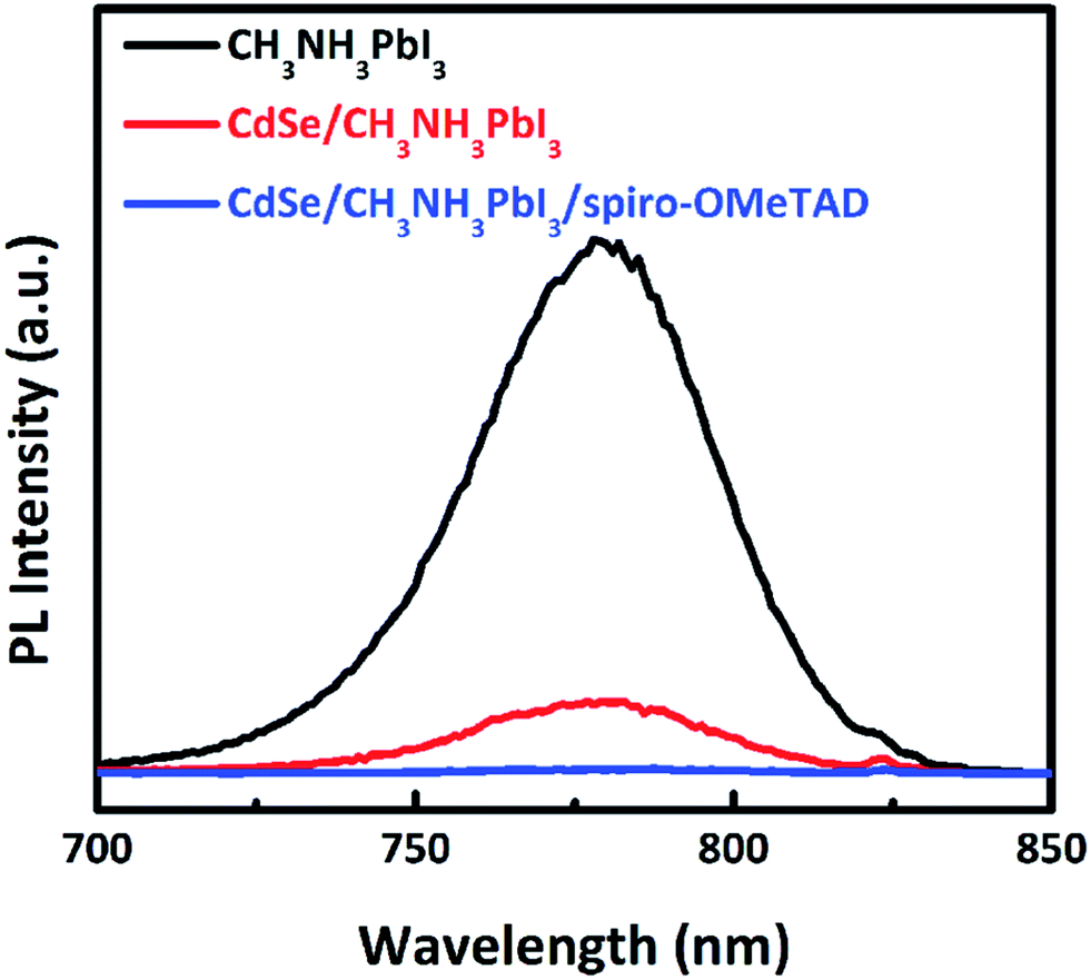 | ||
| Fig. 8 The PL spectra of CH3NH3PbI3, CdSe/CH3NH3PbI3, CdSe/CH3NH3PbI3/Spiro-OMeTAD on glass substrates. The excited wavelength is 600 nm.78 | ||
With an ETL, a high conversion efficiency of ∼8.39% along with a high short circuit current (Jsc) of ∼15.24 mA cm−2, an open circuit voltage (Voc) of ∼0.830 V, and a high fill factor (FF) of ∼0.66 was obtained using Ti-coated ITO/PET substrate. Intensity-modulated photocurrent (IMPS)/photovoltage spectroscopy (IMVS) studies demonstrated that the fabricated flexible PSC had considerably reduced recombination rate and higher charge transfer rate.97
3d. Charge retardation and charge separation using core–shell nanoparticles
TiO2 is the most commonly used ETL in PSC. Chandiran et al. reported 11.5% efficiency by controlling a thin layer of atomic layer deposition (ALD) deposited mesoporous TiO2.98 Using mesoporous TiO2 deposited by a spin-coating method and further changing to core–shell NPs after ALD deposited TiO2, improved the efficiency by retarding charge recombination. The purpose of a thin layer of high band gap materials is to eliminate the contact between the electrode and HTL because the perovskite active layer shows pinholes on thermal treatment during device fabrication, and also to passivate the surface defects on nanoparticulate TiO2 (np-TiO2) mesoporous films. The schematic in Fig. 9 shows that cross-linking core–shell NPs are extended up to the bottom of the electrode.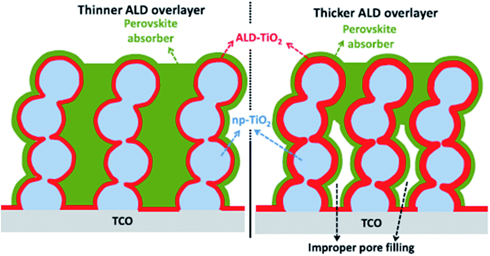 | ||
| Fig. 9 Block diagrams of mesoscopic photoanodes with thinner (left) and thicker (right) ALD TiO2 overlayer (red) deposited on the mesoporous nanoparticle TiO2 (light blue) films. The np-TiO2-ALD TiO2 film is infiltrated with CH3NH3PbI3 absorber (green). For thicker ALD TiO2 overlayers, the pore diameter is reduced and improper pore filling of the perovskite absorber is highlighted (right).98 | ||
Without an ETL, electrons suffer a sudden voltage drop which may degrade the device performance. A novel ITO/TiO2 core–shell nanostructured photoanode was fabricated by Han et al.99 using VLS grown ITO nanowire with ALD deposited TiO2, which gave better electron injection and charge collection efficiency compared with TiO2 ETL. At the same time, this kind of nanostructure gives lower series resistance to the devices, with a lesser diffusion path for charge carrier, and acts as both photoanode and ETL for DSSC as well as hybrid PSC. The same concept was implemented using Al2O3/ZnO nanoparticle to improve the efficiency in PSC.35 Such nanoarchitectures could be implemented for ITO/ZnO, ITO/Al2O3 and ITO/V2O5, etc., because these metal oxides have already been tested as efficient ETL materials and can be deposited by the ALD process.
WO3 is not considered to be an efficient ETM for DSSC.100,101 In comparison with conventional TiO2 ETL, WOx exhibited comparable light transmittance but had higher electrical conductivity. PSCs using WO3 ETL exhibited comparable photoelectric conversion efficiency with TiO2-based PSCs, larger short-circuit current density, and high lower open-circuit voltage.102 However, if a thin layer of TiO2 is coated on the WO3, better electron injection can be observed in comparison with the WO3 alone. This leads to high charge collection efficiency and retards the recombination in PSC. Mahmood et al. reported a mesoscopic WO3/TiO2 nanostructure to get a smooth electron injection to get high Voc and PCE.47 As the FF depends on the series resistance, shunt resistance, and diode characteristics, careful choice of nanostructure, thickness, and pore filling could provide improved FF. A recorded Voc (approx ∼1.3 V) was achieved by tailoring both a low-lying HOMO level as well as the appropriate electronic and optical properties by Edri et al.57 using a TiO2/alumina/CH3NH3PbBr3/PDI structure. Their efficiency was limited, however, to 0.56%.
A high band gap material on m-TiO2 ETL would have reduced the charge recombination rate. PSCs are sensitive to moisture and humidity. It is believed that H2O can decompose CH3NH3PbI3 into PbI2 and CH3NH3I, which can degrade performance of PSC.82,103 The surface of m-TiO2 is prone to H2O/hydroxyl groups, which interact with the NH4 and CH3 in the perovskite layer, and degrade the charge transport.104 Long exposure of m-TiO2 to air and pre heating or UV treatment before fabrication of the perovskite layer can result in the above interface problem. Hence, some previous reports advised TiCl4 treatment, which can prevent such effects in PSC.53 Using a thin layer of MgO on m-TiO2, the recombination resistance can be reduced (Fig. 10).53
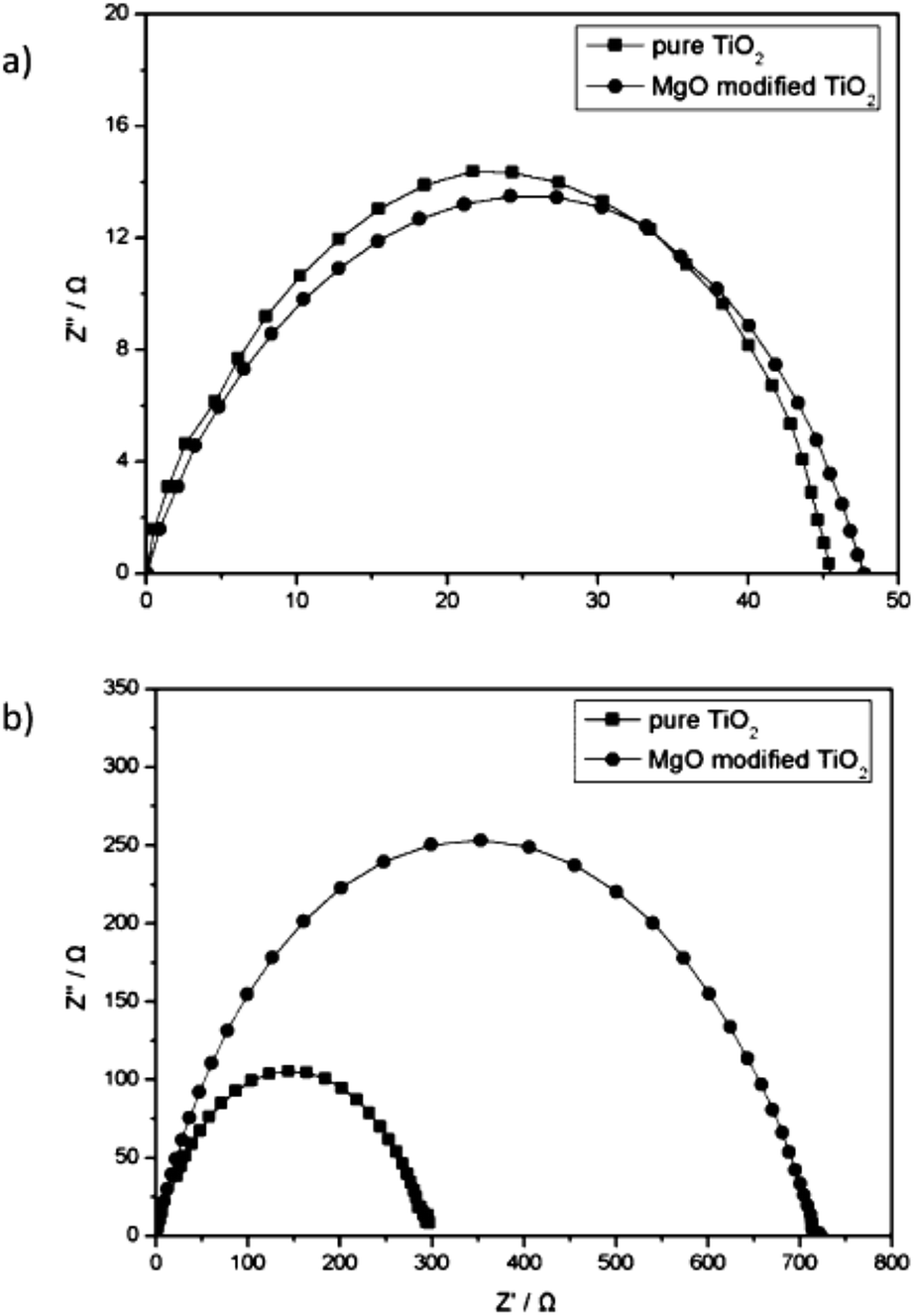 | ||
| Fig. 10 EIS of PSC with and without MgO coating under (a) light illumination and (b) dark conditions.104 | ||
Charge retarding behaviour using heterostructure core–shell nanoparticles is well known in DSCC. Using MgO/TiO2, Al2O3/TiO2, ZnO/TiO2 etc., electron–hole recombination can be suppressed.72,73 MgO-coated TiO2 nanoparticle (NP)-based electron collecting layers were fabricated by Han et al., to prevent charge recombination at the perovskite/TiO2 interface in PSC.73 Open circuit voltage (Voc) and fill factor (FF) with MgO/TiO2 ETL are 4.7% and 6.1% higher, respectively, than with mesoporous TiO2 ETL, and the recombination times for MgO/TiO2 NP-based PSC are about three times longer than that of TiO2 NP-based solar cells. Longer recombination time was achieved by adding an MgO thin layer which retards the electron–hole recombination.71 The detailed mechanism is shown in Fig. 11.
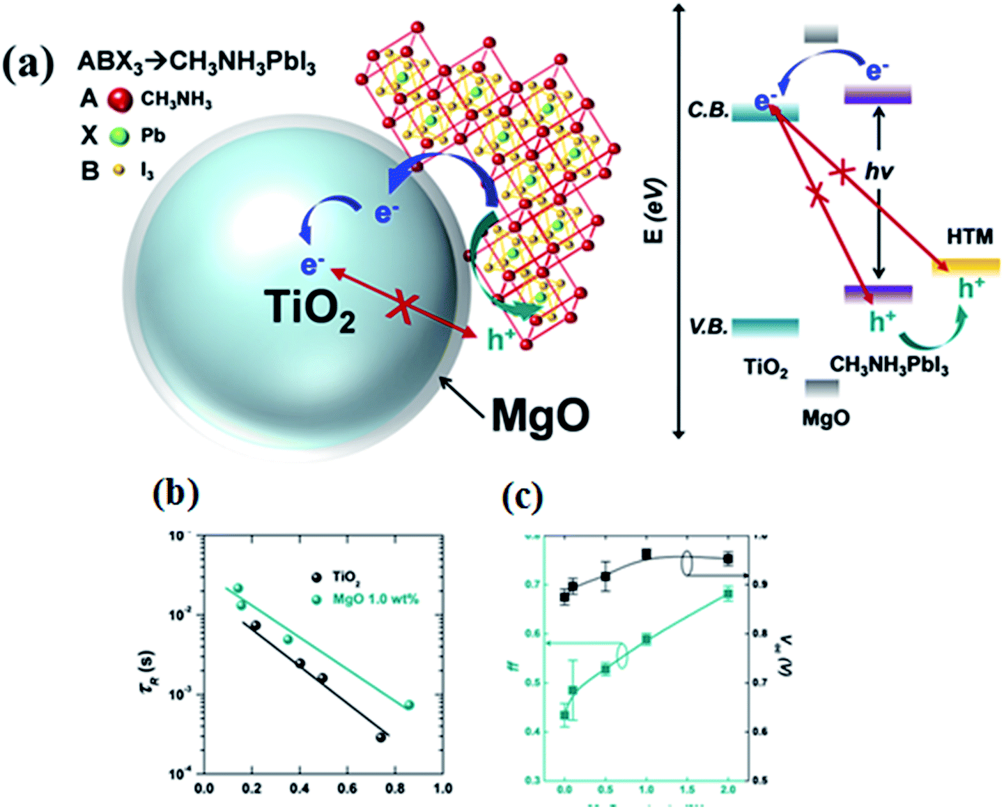 | ||
| Fig. 11 (a) Schematic representation of the charge transfer mechanism in TiO2-based perovskite solar cell with a MgO layer, band energy diagram of the MgO/TiO2 core–shell NP-based perovskite solar cell, (b) electron lifetime of MgO/TiO2 core–shell NP-based perovskite solar cells compared with TiO2 NP-based perovskite solar cells and (c) open circuit voltage (Voc) and fill factor (FF) of the MgO/TiO2 core–shell NP-based perovskite solar cell with varying magnesium methoxide concentrations (0.1 wt%, 0.5 wt%, and 2.0 wt%).73 | ||
3e. Doping effect
It is well known that a photoelectrode can efficiently absorb a photon and provide better band alignment to the charge, which can inject to the electrode. Using Y-TiO2 (0.5% Y) can increase the conduction band edge near to the conduction band of perovskite.105 Mahmood et al. also reported Al doped ZnO as an efficient ETL using an electrospraying method which effectively enhances the charge collection efficiency.106N-type doping leads to an increase in the conduction band edge which can efficiently decrease the charge recombination process. Several n-type dopings have been reported in TiO2 as well as ZnO. Pure anatase mesoporous TiO2 was used as ETL material in the initial stages of PSC research. The band gap of TiO2 is about 3.2 eV with HOMO and LUMO situated at 3.2 eV and 5.4 eV, respectively, which is best fit to the energy level diagram. However, doping to the TiO2 improves the conduction band edge as well as the band gap TiO2. For this reason, n-type doping in ETL gives a smooth electron injection from the perovskite layer to ETL (Fig. 12).
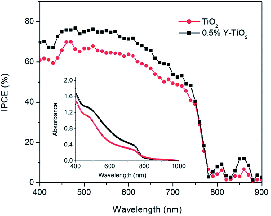 | ||
| Fig. 12 Incident photon-to-electron conversion efficiency spectra of devices based on 0.5% Y-TiO2 (black) and TiO2 (red). The inset shows the UV-Vis absorbance spectra of 0.5% Y-TiO2/CH3NH3PbI3 and TiO2/CH3NH3PbI3 electrodes.34 | ||
In this way, the Voc can be improved to shorten level, which would raise the FF, and consequently the PCE. n-type doping in TiO2 can be achieved using a number of elements. Using Sn doped TiO2, Zhang et al.51 tuned the band gap of TiO2 and improved the efficiency up to 67%. By n-type doping, the conduction band edge can be increased, which can suppress recombination of electron and hole and provide a smooth electron injection. Using this concept, many n-type doped TiO2 have been used to get higher Voc. Manseki et al. used Mg doped TiO2 as ETL to increase the band gap of TiO2 and CB edge, leading to improved Voc.52 Their results showed that the band gap increased up to 1 eV which affects the Voc, increasing it from 587 meV to 802 meV. Electron-rich, nitrogen doped ZnO (N:ZnO) NR-based electron transporting materials (ETMs) with enhanced electron mobility produced using ammonium acetate show consistently higher efficiencies by one to three power points than undoped ZnO NRs.107 Using Pb doped TiO2 nanofibre, Xiao et al. reported 9.03% efficient PSC with an HTL.108 Using Al-doped ZnO (AZO) modified ZnO nanorods as ETL, enhanced Voc and PCE were achieved (Fig. 13).109
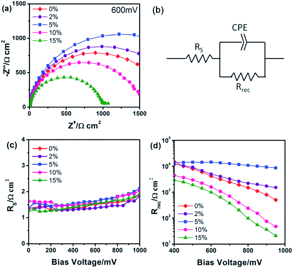 | ||
| Fig. 13 (a) Nyquist plots of the device treated with AZO at different Al doping levels at applied bias (600 mV) under dark conditions. (b) Equivalent circuit employed to fit the IS data. Plots of (c) the series resistance (RS) and (d) the charge transport resistance (Rrec) obtained from IS results as a function of the applied bias.109 | ||
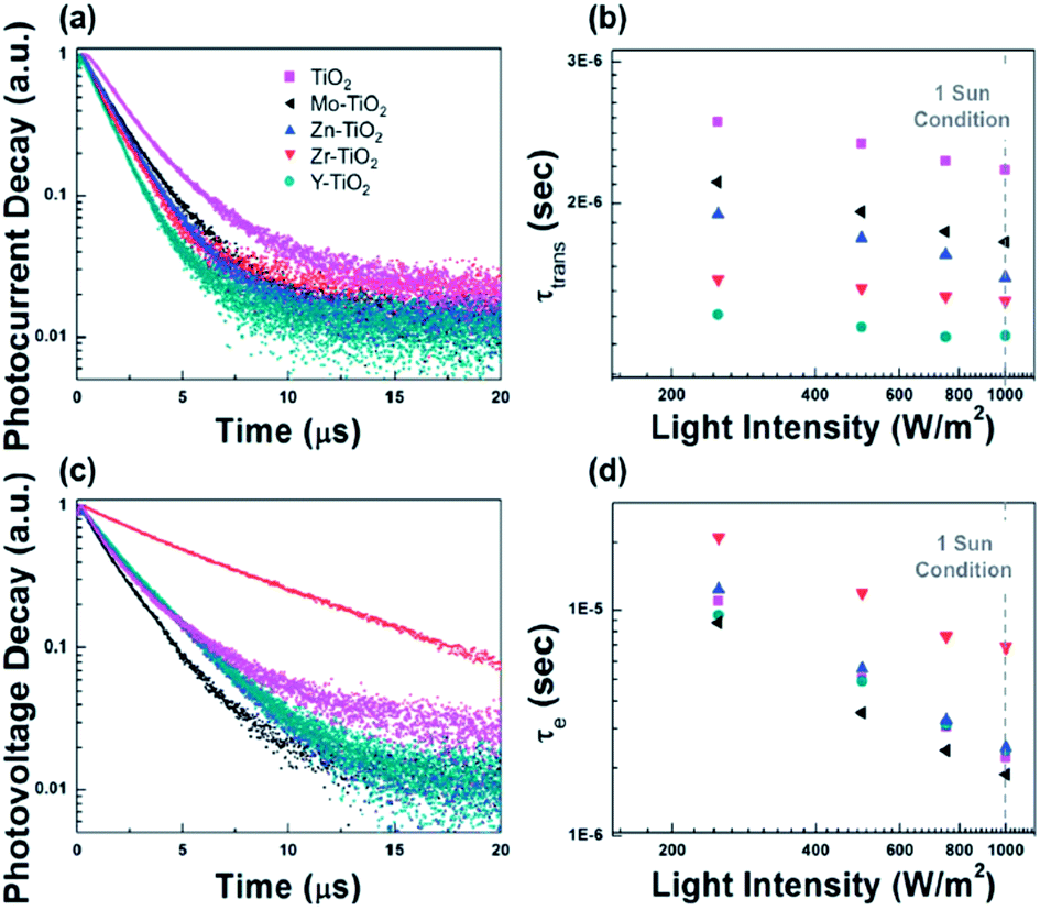
For flexible PSCs, ALD deposited TiO2, ZnO, SiO2, HfO2 and ZrO2 are better options for growth on flexible substrate. However, other methods such as hydrothermal, spin coating, electrospray method spray deposition are good for PSC fabricated on rigid substrates. Using a hydrothermal method, the microstructure can be easily tuned to tune the optical properties and device architecture. The electrospray method is a better choice for growth of many novel nanostructures with multilayer structure for sensitized and solid state PSC.110 Electrospray has many process parameters, and can adjust the thickness as well as morphologies. Magnetron sputtering grown compact ZnO as ETL was deposited by Liang et al.48 They observed 13.4% and 8.03% PCE on ITO/glass and ITO/PET substrate. The sheet resistance of ZnO/ITO/glass was limited to 8.0 ohm per cm2, which gave a low series resistance to the device. At the same time, compact ZnO films by magnetron sputtering mean that the shunt resistance would be high enough to give such high efficiency. A complete list of fabrication methods and their electronic properties is given in Table 1. The HOMO, LUMO, and band gap are also listed and the band energy diagram with respect to perovskite is tabulated. As per theoretical study by Minemoto et al.,67 the band offset between the ETL and perovskite layer should be in the range of 0.0–0.3 eV, to give an optimum Voc, which regulates the FF in PSC. This information is useful for fabricating highly efficient PSC by choosing an optimum thickness, microstructure, doping, and device architecture. Band gap tailing by Nb doping in TiO2 and faster electron injection and electron lifetime was reported by Kim et al.111 They showed light Nd doped TiO2 to have the highest efficiency of 13.4% (Fig. 14).
| Solar cell type | V oc (mV) | J sc (mA cm−2) | FF (%) | PCE (%) |
|---|---|---|---|---|
| PSC-30 | 995 | 21.61 | 66.59 | 14.32 |
| PSC-40 | 1029 | 21.45 | 69.74 | 15.24 |
| PSC-50 | 1049 | 21.58 | 75.94 | 17.19 |
| PSC-65 | 1005 | 21.27 | 72.35 | 15.47 |
 | ||
| Fig. 14 (a) Nyquist plot of the PSCs measured at open-circuit conditions. The impedance spectra measured in the frequency range of 10 mHz to 2 MHz at open circuit potential under 1 sun illumination. (b) tR of the PSCs as a function of Voc. The detailed measurement conditions of tR are the same as those of the tc measurements (Fig. 6).111 | ||
3f. Induced dipole effect: the role of polymer on ETL
Introducing a dipole layer at the TiO2/perovskite interface can efficiently separate the electron and hole by controlling the polymer thickness, which can reduce the charge recombination in a solar cell.104 The existence of oriented permanent dipoles at the TiO2/perovskite interface is consistent with the hypothesis of an ordered perovskite layer, close to the oxide surface without using polymer.112 Photoinduced absorption (PIA) and electron absorption (EA) study confirmed that either non-oriented permanent dipoles and/or likely expectable bulk polarization effects, contribute to the Stark signal. Sometimes a thin polymer layer induced a dipole moment between ETL and the perovskite layer. Polyethylene amine (PEI) which is used as a surfactant to grow ZnO nanostructure is conserved for induced dipole moment.107 Using PEI nanolayer, smooth electron injection was observed by inducing a dipole layer at the PEI/TiO2 (ref. 71) or PEI/ZnO107 interface, which can increase the conduction band edge to give smooth electron injection. Moreover, a dipole layer can efficiently separate the electron from the perovskite absorber. Zhou et al. used the same concept to achieve high efficiency, with Y-TiO2 to improve the efficiency.71 Polymers induced the dipole effect and their effects on device performance in different device structures are summarized in Table 2 (Fig. 15).| Polymer | Device structure | J sc (mA cm−2) | V oc (V) | FF | PCE (%)Ref |
|---|---|---|---|---|---|
| PEI/Y-TiO2 | ITO/PEIE/CH3NH3PbICl/Spiro-OMeTAD/Au | 22.75 | 1.13 | 0.750 | 19.03 (ref. 71) |
| PEI/N:ZnO | ITO/ZnO/PEI/CH3NH3PbI3/SpiroOMeTAD/Au | 21.5 | 9.645 | 0.700 | 16.1 (ref. 107) |
| ZnO/PCBM | ITO/PEDOT:PSS/CH3NH3PbI3−xClx/PCBM/ZnO/Ag | 16.0 | 0.95 | 0.745 | 11.3 (ref. 145) |
| Perylene-diimide/PCBM | ITO/PEDOT:PSS/CH3NH3PbI3−xClx/PCBM/PDINO/Ag | 18.8 | 0.95 | 0.785 | 14.0 (ref. 145) |
| PEI/PCBM | FTO/PEI/PCBM/MAPbI3/PTAA/Au | 21.8 | 0.98 | 0.720 | 15.3 (ref. 138) |
| Rhodamine 101/LiF | ITO/PEDOT:PSS/CH3NH3PbI3−xClx/rhodamine 101/LiF/Ag | 17.72 | 1.01 | 0.730 | 13.2 (ref. 134) |
| PCBM:polystyrene | FTO/NiO/CH3NH3PbI3−xClx/PCBM:PS)/Al | 15.62 | 1.07 | 0.640 | 10.68 (ref. 39) |
| PN4N | ITO/PEDOT:PSS/CH3NH3PbI3−xClx/PCBM/PN4N/Al | 20.61 | 1.0 | 0.725 | 15 (ref. 146) |
| PFN | ITO/PEDOT:PSS/CH3NH3PbI3−xClx/PCBM/PFN/Al | 20.47 | 0.98 | 0.552 | 8.7 (ref. 146) |
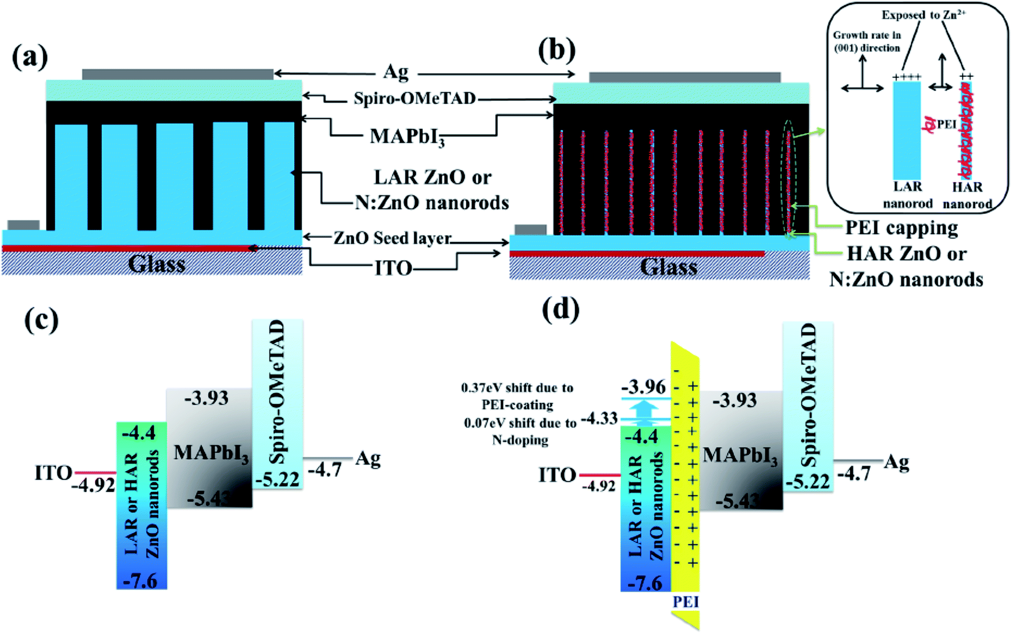 | ||
| Fig. 15 Schematics of device structure based on (a) conventional low aspect ratio (LAR) NR arrays, and (b) high aspect ratio (HAR) NR arrays with additional PEI coating (the inset shows the schematic representation of PEI as a capping agent to control nanorod growth). Energy diagrams of the devices based on (c) LAR or HAR NRs without PEI coating and (d) LAR or HAR NRs with PEI coating. The conduction band energy of ZnO was lowered by 0.07 eV by nitrogen doping and by 0.37 eV by dipole formation by the PEI layer.107 | ||
3g. Nanostructured electron transport layer
Surface coverage of the perovskite layer by the ETL is one of several issues in PSCs. Compact TiO2 deposited by ALD or a spin-coated m-TiO2 compact layer is better for vapour-deposited perovskite layer, as reported by Snaith's group for planar heterojunction (PHJ) PSC. Chlorine inclusion or chlorine addition in either a one-step or two-step method gives better surface coverage on m-TiO2. This technique provides the PHJ PSC. However, a nanostructured ETL has been found to be best for iodine precursor or mixed halide precursors in which the perovskite crystal is in the range 200–500 nm. Controlling the aspect ratio of nanowires allows perovskite to infiltrate into the ETL, giving a direct path for the charge carrier to be collected by the electrode.Generally, the PSC needs a mesoporous ETL, compact ETL, or a scaffold material for growth of the perovskite absorber. The most common practice is to use a commercially available mesoporous TiO2 layer, which has superior electrical properties because the mesoporous TiO2 is deposited easily by spin-coating, but the thickness and roughness cannot be easily controlled. Also, perovskite is sometimes inserted into the TiO2 layer and this cannot be distinguished using a cross-sectional scanning electron microscope. A number of reports describe such intermixed TiO2 and perovskite layers using the 1S and 2S methods. The microstructure of CH3NH3PbI3 has particle size in the range of 100–500 nm with large pore size. When the HTM is deposited on the perovskite layer, the HTL may insert into the gaps, touching the ETL and providing a shunt path. Consequently, the efficiency of the solar cell is degraded. The effects of morphology and pore filling of mesoporous TiO2 layer and perovskite layer in terms of device performance were studied by Nanova et al.69 TEM-EELS (electron energy loss spectroscopy) measurements were used to study the mechanism and optimum pore structure of TiO2/perovskite. A finer grain of TiO2 efficiently accompanies the perovskite, resulting in an interlinked structure and better PCE. Hence, an over-layer perovskite absorber is needed to overcome the problems described above (Fig. 16).
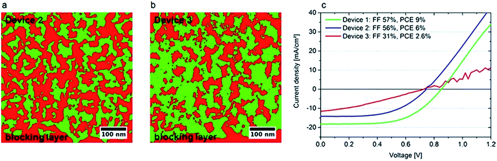 | ||
| Fig. 16 Correlation between morphology and device characteristics. (a) Device 2 exhibits a compact and well-connected TiO2 network. (b) The TiO2 in device 3 is a much finer grained structure (very small and unconnected red domains). (c) I–V characteristics of the devices. The higher fill factors of devices 1 and 2 can be correlated to the well-connected TiO2 network and hence better electron transport properties.66 | ||
Fast electron transport and charge collection is possible using nanostructured ETL materials such as nanowire, nanosheets, and nanoneedles. These NSs provide better charge injection and unidirectional charge transport. Smooth injection is the key point at the ETL and perovskite interface, which must satisfy the condition that the LUMO of the ETL is lower than that of the perovskite. However, the CH3NH3PbI3 and (Cl, Br) doped CH3NH3PbI3 (CH3NH3PbClx, CH3NH3PbClxBryI1−y) were found to be beneficial because of the optimum band gap giving broad absorption in the UV-Vis region and high extinction coefficient.113–115 A schematic band energy level diagram of hybrid perovskite materials is presented in Fig. 1. To provide a smoother path for the electron the LUMO level of the ETL should be lower than the LUMO level of the intrinsic layer, and the HOMO level should be higher than that of the intrinsic layer.
Nanostructure ETL such as nanowire and nanorods were found to be beneficial for charge collection. A better surface morphology, roughness, and nanoarchitecture give efficient electron injection and a short carrier path for the electron. Transition metal oxides (TiO2, ZnO) can have a variety of nanostructures, and can be easily doped by a number of elements to increase/decrease the Fermi level, which affects the electron injection efficiency and consequently leads to enhanced transport properties and better charge collection efficiency. Park et al. used ZnO nanorods to efficiently collect the electron from the lower wavelength region.46
Using a dense compact TiO2 layer, the series resistance of photovoltaics (PV) was improved by Ke et al.116 Their approach was to minimize the series resistance, giving a higher recombination time of the PSC. They achieved about 15.07% efficiency with Voc up to 1.04 V. Using electrospun deposited TiO2 nanofibre of different TiO2 thicknesses, Dharani et al. reported Voc = 844 mV with PCE = 9.8%.50 They predicted that Voc decreased with increasing fibre thickness.
Hydrothermally deposited one-dimensional TiO2 array rather than a mesoporous TiO2 layer is a better ETL for PSC. A schematic of a 1D TiO2/perovskite solar cell is presented in Fig. 17.50 The schematic gives misleading information that the HTL is in contact with the TiO2 ETL, which might have resulted in high shunt resistance and low recombination time, so degrading the solar cell performance. Hence, the J–V curves did not maintain the current with increasing Voc. At the same time the series resistance is comparatively high using long TiO2 nanorod. A highly efficient 1D TiO2 can be fabricated by proper choice of thickness of TiO2 and doped TiO2 nanorod with excellent pore filling and over layer perovskite material with controlled pore size. Large pore size and particle size of perovskite films allow insertion of the HTL into the TiO2 ETL, giving low shunt resistance which gives low FF.
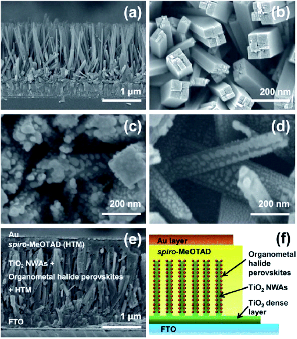 | ||
| Fig. 17 Cross-sectional (a) and top (b) view SEM images of TiO2 nanowire arrays (NWAs) synthesized on FTO substrates. SEM images of CH3NH3PbI2Br (c) and CH3NH3PbI3 (d) spin-coated on TiO2 NWAs. (e) Cross-sectional SEM image of the TiO2 NWAs/perovskite sensitizer/spiro-MeOTAD hybrid photovoltaic cell. (f) Schematic illustration of the hybrid solar cell. | ||
Control over nanostructure ETL with different morphology and size shows better electron injection, electron transfer, and charge collection efficiency.36,37,100 The thickness and gap between nanorods should be controlled to decrease the series resistance and increase the shunt resistance. A non-porous ETL needs a thin compact hole blocking layer for better film growth. Increasing the nanowire length provides higher series resistance and also gives a large carrier path to extract the electron. If the nanowire size can be controlled, the perovskite can be infiltrated into the nanowire gaps, which would compensate the series resistance by several orders. At the same time, a proper morphology must be considered to obtain high efficiency. The microstructure cannot be easily controlled using the spin coating process. Extra additives or doping is required to initiate a large number of nucleation sites which can grow nanocrystalline perovskite nanoparticles with high surface coverage. This method allows high shunt resistance to get high fill factor with high external quantum efficiency (EQE).
By controlling the photoelectrode thickness and perovskite thickness, Dhar et al. efficiently controlled the charge injection to the photoelectrode. A PSC of 12% efficiency was fabricated using novel (001)-oriented nanoplatelets of anatase thin film as the photoanode.117 A thicker ETL material provides a longer diffusion path for the electron to reach the electrode, which limits the charge collection efficiency and also transmittance of the incident photon decreases with increasing thickness. So when designing an ETL, the optimum thickness should be considered. Oh et al. reported ternary Zn2SnO4 (ZSO) as the electron-transporting electrode of a CH3NH3PbI3 PSC as an alternative to the conventional TiO2 electrode.118–120 They obtained different thicknesses of ZSO compact layer or ZSO mesoscopic layer using the spin coating method.118 They observed that transmittance of ZSO films had negligible effect on increasing thickness. In addition, time-resolved and frequency-resolved measurements revealed that the ZSO-based PSC exhibits faster electron transport (∼10 times) and superior charge collection capability compared with its TiO2-based counterpart with similar thickness and conversion efficiency. Using Zn2SnO4/PVP nanofibres, Mali et al. reported 7.3% efficiency (Fig. 18).
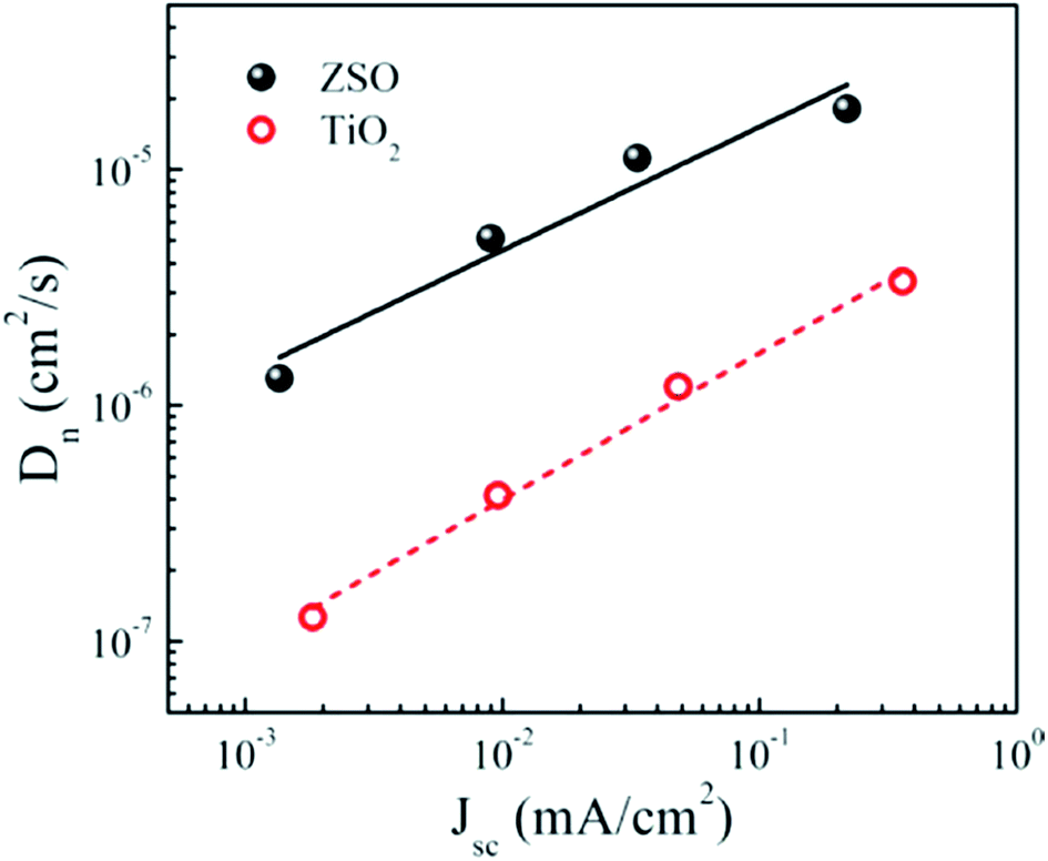 | ||
| Fig. 18 Electron diffusion coefficients of the ZSO-based perovskite solar cell with the highest conversion efficiency. Electron diffusion coefficients of a TiO2-based perovskite solar cell with similar thickness (∼300 nm) and conversion efficiency (∼7%) are also presented for a comparison.118 | ||
3h. Additive controlled enhanced charge injection/collection
Wang et al.121 used a range of additives from divalent (II), trivalent (III), and tetravalent (IV) to hexavalent (VI) acetylacetonate in TiO2 to demonstrate efficient charge injection. Also, different substrate treatment of m-TiO2 was found to be beneficial for crystallization behaviour of the perovskite layer.117 Amino acid-modified TiO2 ETM has more efficient charge transfer from perovskite to TiO2.122Using ZnO/PCBM ETL in a PHJ PSC, trap-assisted recombination was lowered by several orders.123 Interface modification plays a crucial factor by passivation or deposition of polymer on inorganic ETL, found to enhance the efficiency of PSC by improving the electron transport/extraction. The aim of using PCBM on ZnO123 and TiO2 (ref. 124 and 125) is to adjust the quasi Fermi level of ETL and HTL, as the Voc of the PHJ PSC is decided by the energy-level offset between the quasi Fermi levels of the ETM and the HTL adjacent to the perovskite active layer.126,127 In addition, efficiency can also be enhanced by use of an induced dipole moment to enhance charge collection of electron and reduce charge recombination (Fig. 19).
 | ||
| Fig. 19 (a and c) Photocurrent and photovoltage decay of devices employing the TiO2 ETL incorporated with different acetylacetonate-based additives and (b and d) the related carrier transport lifetime and electron lifetime. Intensity is shown in log scale and 1 sun condition is equivalent to 1000 W.121 | ||
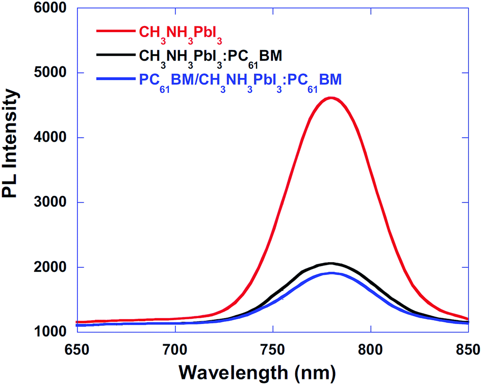
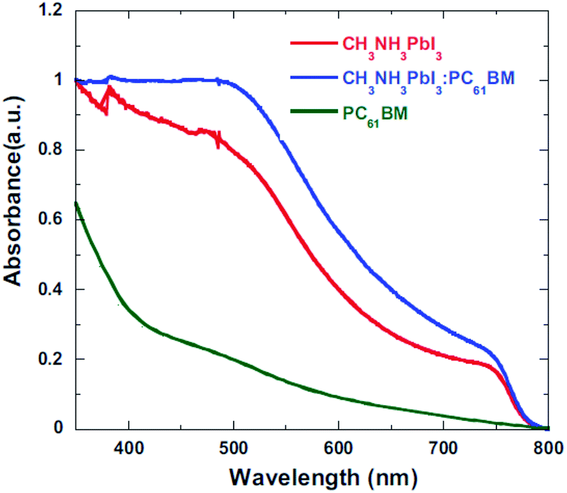
The role of the ETM/ETL is to collect electrons efficiently and retard the hole toward the HTL. Efficient charge injection of electron or hole can be analysed by time-resolved photoluminescence decays and the photoluminescence quantum efficiencies of the perovskite films on ETL. With a BHJ PSC architecture, using PC61BM/CH3NH3PbI3:PC61BM composite thin films, the device performance was improved by means of excellent charge collection. Fig. 21 shows the photoluminescence (PL) spectra of the pristine CH3NH3PbI3, CH3NH3PbI3:PC61BM, and PC61BM/CH3NH3PbI3:PC61BM thin films. PL quenching was observed in CH3NH3PbI3:PC61BM and PC61BM/CH3NH3PbI3:PC61BM composites compared with CH3NH3PbI3, which confirms efficient exciton dissociation at “donor/acceptor” interfaces and subsequently electron extraction. With this concept, reduced electron–hole pair recombination and faster charge extraction/collection was obtained in the conventional BHJ PSCs.124 At the same time, this composite film shows higher absorbance than the CH3NH3PbI3 (Fig. 20–22).
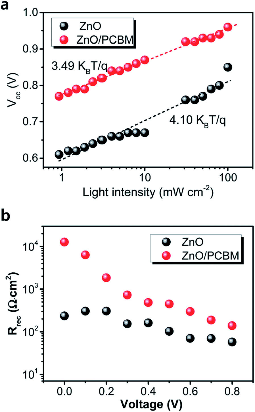 | ||
| Fig. 20 (a) Light-intensity dependence of the Voc of the perovskite solar cells with ZnO and ZnO/PCBM. The lines represent the best fits to the data, for which the slope is indicated. (b) Recombination resistance at different applied biases extracted from IS characterization of the perovskite solar cells.128 | ||
 | ||
| Fig. 21 Photoluminescence (PL) spectra of the pristine CH3NH3PbI3, CH3NH3PbI3:PC61BM, and PC61BM/CH3NH3PbI3:PC61BM thin films.124 | ||
 | ||
| Fig. 22 Absorption spectroscopy of CH3NH3PbI3, CH3NH3PbI3:PC61BM, and PC61BM/CH3NH3PbI3:PC61BM thin films.124 | ||
3i. Plasmonic nanoparticles in conventional electron transport layer
Plasmonic NPs improve absorption by scattering light using metal nanoparticles excited at their surface plasmon resonance. Using sandwiched TiOx–Au–TiOx ETL with a plasmon-mediated hot carrier injection from the Au-NPs to TiOx, Yuan achieved PCE of 16.2%.129 Using binary Au–Ag popcorn metal NPs, absorption of both TiO2 and perovskite active layer improves through localized surface plasmon (LSP), which gives higher efficiency (Fig. 23).130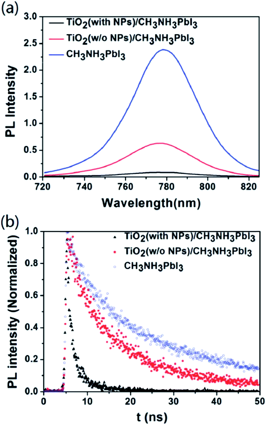 | ||
| Fig. 23 (a) Photovoltaic performance of 25 individual devices (red: devices with popcorn NPs; black: control devices). (b) J–V curves of the best-performance perovskite device with and without popcorn NPs, respectively.130 | ||
In a similar way, a DMAPA-C60 layer on PCBM lowers the work function (WF) by inducing an interface dipole moment, creating a selective quasi-ohmic contact at the interface with Ag (Fig. 24).131 This formation of a dipole layer by either PEI or DMAPA-C60 directly impacts on the WF of electrode and suppresses the energy barrier between the ETL and electrode.104
A remarkable FF of 86.7% with enhanced electron extraction efficiency was achieved by bulk heterojunction (BHJ) pero-HSCs fabricated by blending perovskite materials with fullerene derivatives A10C60 (Fig. 25).132
 | ||
| Fig. 24 Different polymer additives used in organic electron transport layers.131 | ||
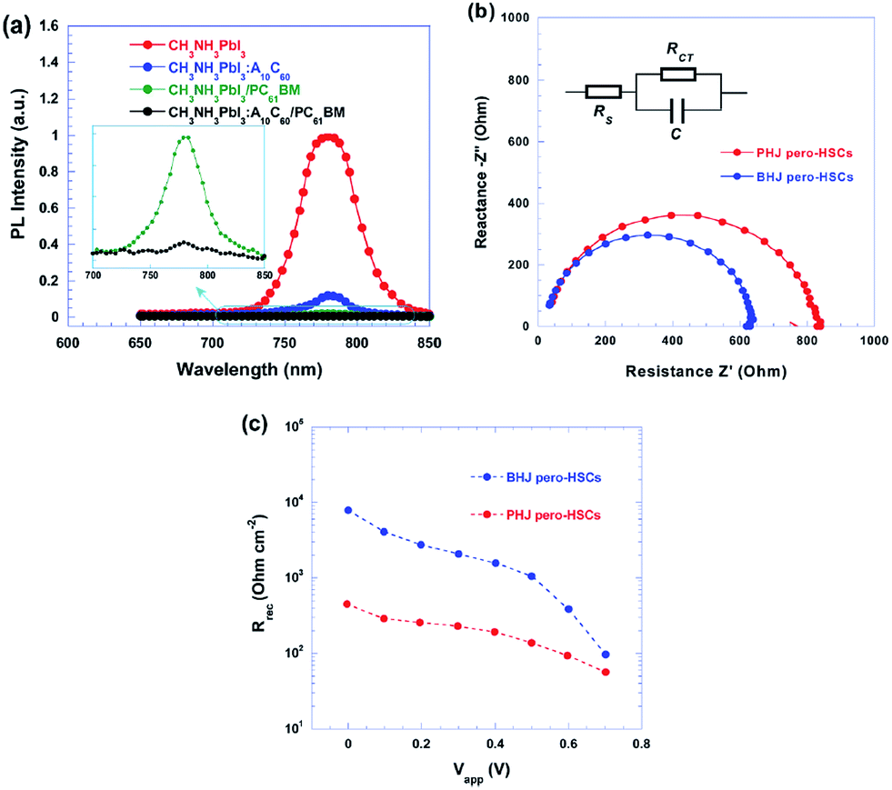 | ||
| Fig. 25 (a) PL spectra of CH3NH3PbI3, CH3NH3PbI3:A10C60, CH3NH3PbI3/PC61BM and CH3NH3PbI3:A10C60/PC61BM thin films; insets, enlarged PL spectra of CH3NH3PbI3/PC61BM and CH3NH3PbI3:A10C60/PC61BM thin films. (b) Nyquist plots of PHJ and BHJ pero-HSCs measured in the dark and at an applied voltage close to the open-circuit voltage of the pero-HSCs. (c) Recombination resistance resulting from impedance spectrometry measurements fitted for different applied biases at 1 sun illumination.132 | ||
Limitation of the band gap and absorbance in the UV-Vis region and their photoresponses limits the device performance. It has been confirmed that the band gap of MAMeX3 can be tuned by changing M, A, Me, X, or MA; however, devices suffer in terms of Jsc, Voc, and FF. By implementing another photoactive material in a PSC, which could behave as both ETL and active material, better performance would be achieved than using a material with single active layer. Poly(diketopyrrolopyrrole-terthiophene) (PDPP3T) is a typical low-band gap polymer which is used as an active material in PSCs. It also has lower HOMO level than that of hybrid perovskite material, enabling use as the ETL in PHJ or BHJ solar cell.133 By implanting PDPP3T–PC61BM BHJ into PSCs, the absorbance of a cell was successfully enhanced in the long-wavelength region. Fig. 26 shows a comparison of absorbance of CH3NH3PbI3/(PDPP3T–PC61BM) blend films (Fig. 26).
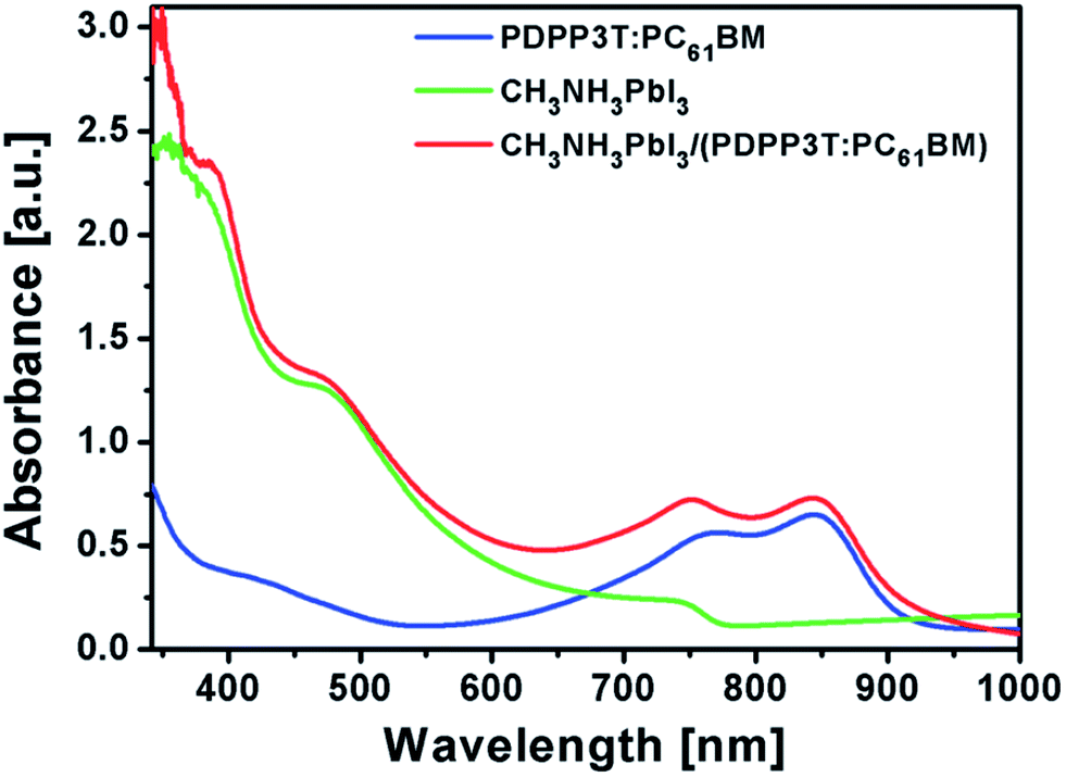 | ||
Fig. 26 Comparison of absorption spectra for PDPP3T–PC61BM (1![[thin space (1/6-em)]](https://www.rsc.org/images/entities/char_2009.gif) :2) blend film, CH3NH3PbI3 film, and CH3NH3PbI3/(PDPP3T–PC61BM) (1:2) bilayer film.133 :2) blend film, CH3NH3PbI3 film, and CH3NH3PbI3/(PDPP3T–PC61BM) (1:2) bilayer film.133 | ||
Even when the band energy level of PCBM matches with cathode, some interfacial issues can arise such as interfacial trap and defect states, which significantly affect the charge collection. Interlayer polymers can overcome these difficulties and help to achieve smooth energy level alignment. These polymers can help electrons to efficiently collect at the cathode of PSCs in cases of energy mismatch between PCBM and cathode. In addition, interlayers can provide better surface roughness for electrode deposition, which ultimately affects the charge collection. It is believed that polymer ETL passivates defects of the perovskite layer, which might not occur when using inorganic ETL/scaffold. Another advantage of polymer ETL is that it does not require high temperature deposition.
In general, a compact TiO2 layer is used as the hole blocking layer (HBL) in m-TiO2 based PSCs. The BCP layer on PCBM ETL acts in the same way as the TiO2 compact layer does in inorganic ETL. By employing double interfacial layers (rhodamine101/LiF), Sun et al. achieved better efficiency than that of PCBM/LiF and PCBM/rhodamine 101.134 Moreover, zwitterions with positive and negative charges on the same molecule can lower the work function of electrodes by formation of interface dipoles.135,136 In the same way, this was achieved using interlayer PEI on TiO2 [Yang] or ZnO [Mahmood].
The addition of PS aids formation of a highly smooth and uniform PCBM on the perovskite active layer that is more effective in preventing undesirable electron–hole recombination between the perovskite layer and the top electrode.39
3j. Functionalization
By introducing glycine, an amino acid, as a coupling agent, better surface morphology of perovskite films was observed, which ultimately reduced the transport resistance (Fig. 28) and improved the Jsc from 14.42 to 19.54 mA cm−2 (Fig. 27).137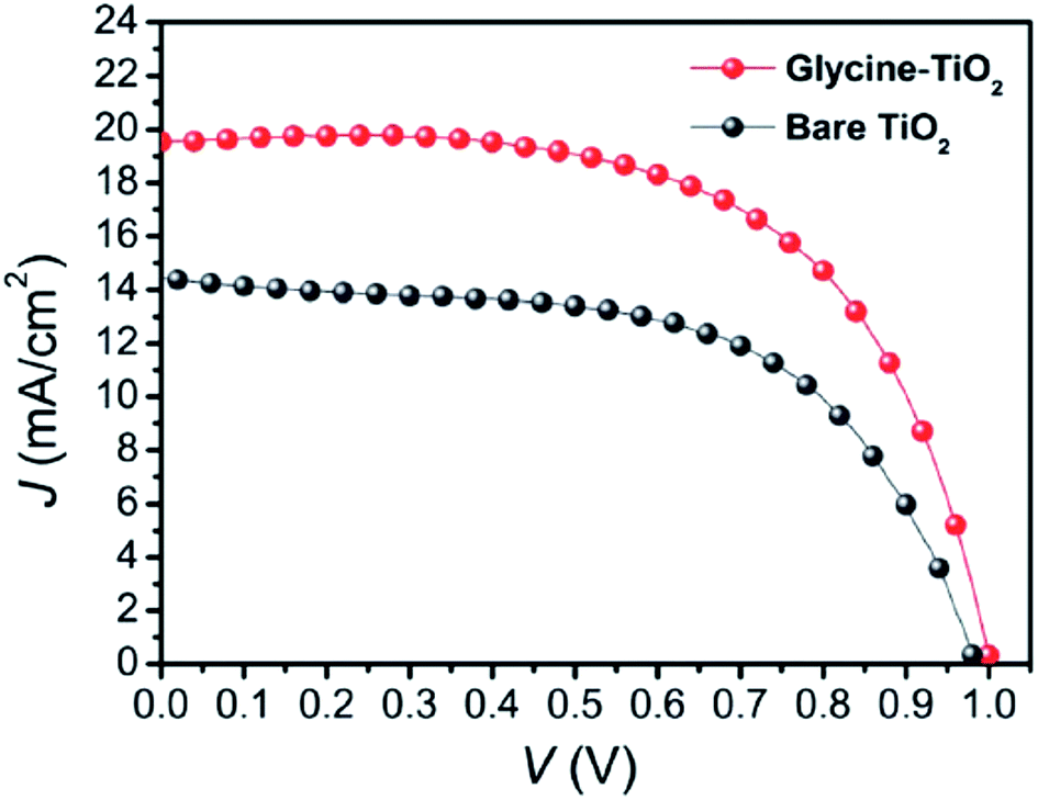 | ||
| Fig. 27 J–V curves of the best perovskite solar cells with bare TiO2 (dark gray curve) and glycine-treated TiO2 (red curve).137 | ||
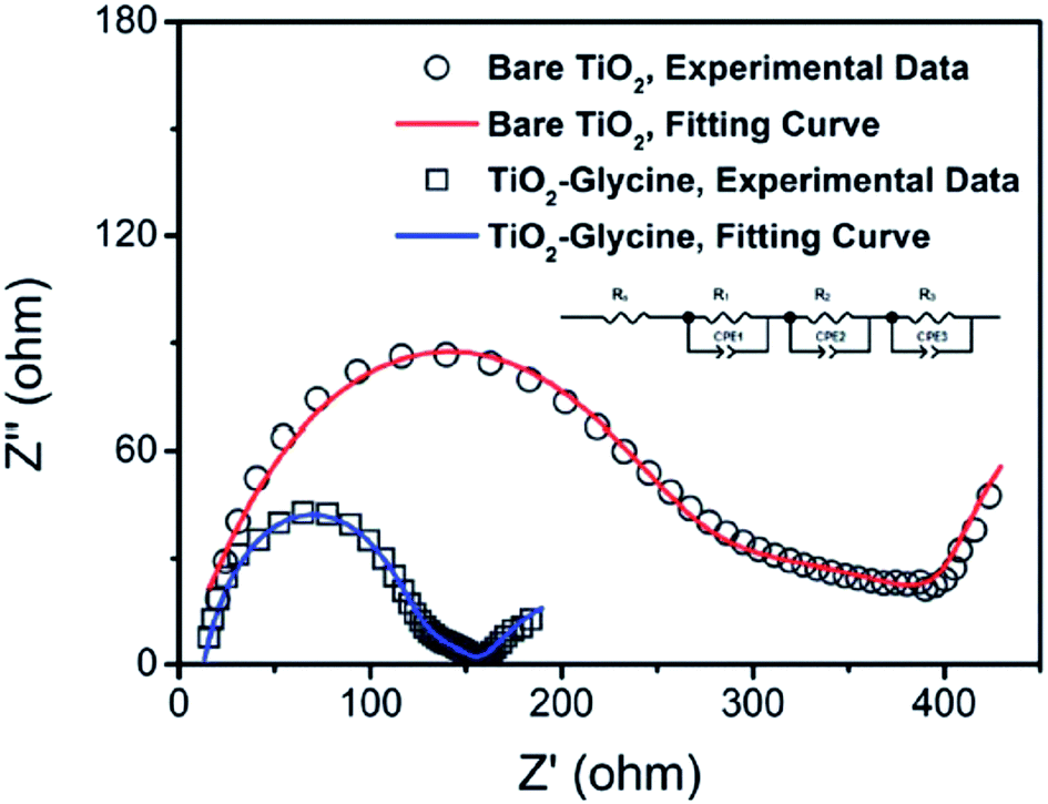 | ||
| Fig. 28 Nyquist plots of perovskite solar cells based on bare TiO2 (symbol B) and glycine-treated TiO2 (symbol). Symbols are experimental data and solid lines correspond to the fitting results using the equivalent circuit shown in the inset figure. EIS spectra were recorded using a potentiostat/galvanostat instrument (PGSTAT 302N, Autolab) equipped with a FRA2 module under constant light illumination of 100 mW cm2. A DC applied bias voltage was set at open circuit voltage of the perovskite solar cells with a sinusoidal ac potential perturbation of 15 mV over a frequency range from 1 MHz to 0.01 Hz.137 | ||
Conjugated polymer electrolytes (CPEs) are another class of efficient interface materials that form the electron dipole moment at the interface of either metal/ETL or ETL/perovskite. These concepts of interface engineering have been regarded as beneficial for improving the device performance by charge collection, extraction/injection. Ryu et al. achieved PCE of about 15% in FTO/PEI/PCBM/MAPbI3/PTAA/Au PHJ PSC.138 To improve efficiency, well-organized mesoporous TiO2 photoelectrodes were fabricated by block copolymer-induced sol–gel assembly by Sarkar et al.139
V oc can be increased by reducing electron–hole recombination occurring at the HTL/ETL inside a perovskite pinhole. Functionalizing the ETL/scaffold by organic/polymer molecules would provide better recombination resistance. Different concentrations of 3-aminopropyl (3-oxobutanoic acid) functionalized silica nanoparticles were used to improve Voc and PCE by a one-step solution process.140 The advantage of functionalized SiO2 NPs over compact TiO2, is that hole transfer is hindered from the perovskite as well as the HTL. The functionalized SiO2 lowers the conduction band edge to give a smooth electron injection to the metal electrode. Absorption of perovskite films was improved in a broad range of light spectrum by employing 3-aminopropyl (3-oxobutanoic acid) functionalized silica nanoparticles at different concentrations, as shown in Fig. 29.
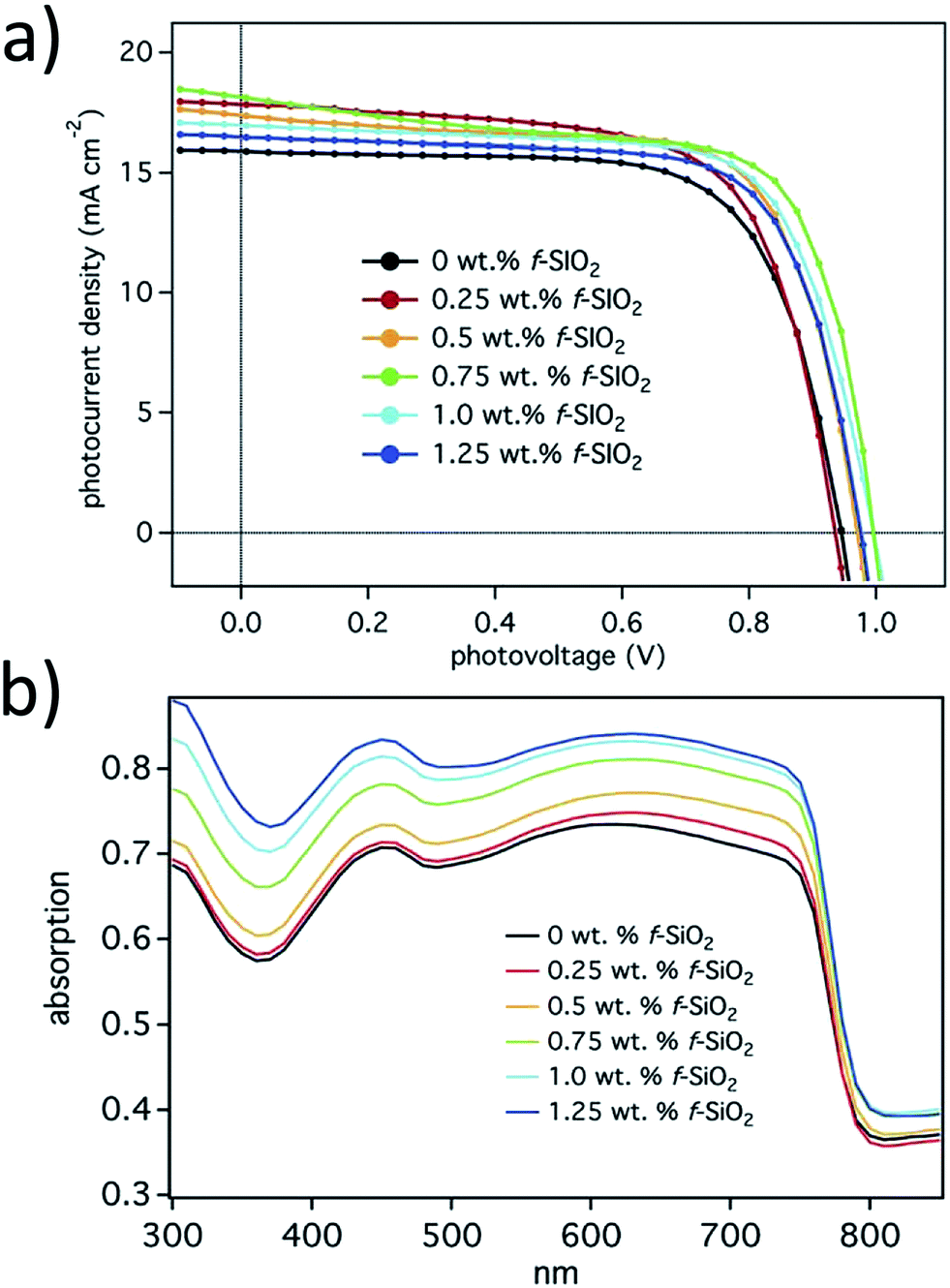 | ||
| Fig. 29 (a) I–V curves of best performing devices for each f-SiO2 wt%; (b) UV-Vis reflectance spectra of perovskite films with varying f-SiO2 wt% loadings.140 | ||
C60SAM functionalized mesoporous TiO2 as ETL has shown recorded efficiency of ∼11.7% in a perovskite-sensitized solar cell using Spiro-OMeTAD as a transparent hole transporter.141 In this approach, C60SAM functionalized mesoporous TiO2 enhances both the absorption and the electron injection. It was observed that the contact between the perovskite and the planar n-type TiO2 charge collection layer was not effective for electron transfer. Modifying this contact with an organic electron-accepting fullerene self-assembled monolayer (C60-SAM) modified TiO2, significantly enhanced the electron transfer.141 Most of the interlayer organic/polymer molecules passivate or inhibit the formation of trap states at the interface, on the TiO2 surface through the anchoring group. This results in reduction of the non-radiative recombination channels at this interface.142 Through electroluminescence (EL) studies, Wojciechowski et al. showed a 5/10-fold increase in the electroluminescence signal for a fullerene-modified sample compared with a standard cell, indicating that the non-radiative recombination at the heterojunction was reduced with the C60-SAM treatment. The observed increase in EL intensity also suggests that the functionalization led to a reduction of interface defect sites, either on the TiO2 or in the perovskite, which would otherwise cause non-radiative recombination of injected carriers. This is consistent with recent results by Q. Wang et al., who suggested that fullerene can passivate trap states in the perovskite itself. Using triple cathode buffer layers consisting of PCBM/C60/LiF, a PCE of up to 14.24% was achieved with excellent stability (Fig. 30).143
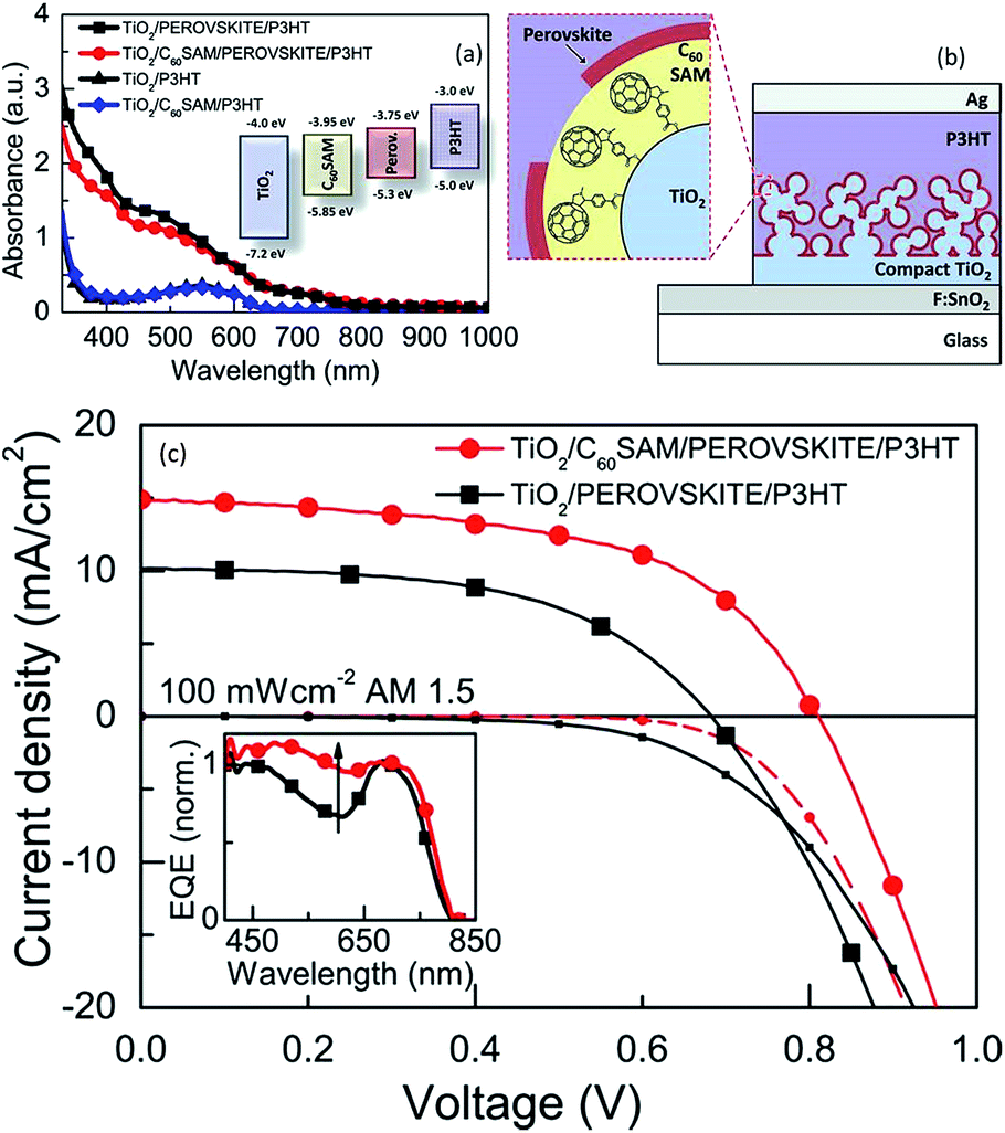 | ||
| Fig. 30 (a) Absorption spectra of P3HT and perovskite films with and without C60SAM fullerene functionalization. The materials were cast on glass substrates which had been coated with a 600 nm thick m-TiO2 layer. Inset: energy levels of the system components relative to vacuum. (b) Schematic of the device 4d. (c) Microstructure and morphology effect (c) J–V characteristics taken under AM1.5 simulated sunlight (100 mW cm−2 irradiance) and in the dark for devices with and without C60SAM fullerene functionalization. Inset: external quantum efficiencies (EQE) for the same devices.141 | ||
Growing interest in PSCs and increased knowledge on how to improve their efficiency by manipulating the microstructure, morphologies, doping, and device architecture has resulted in development of several techniques to fulfil these requirements. For example, several methods have been suggested to deposit ETM/ETL. The most common technique is spin coating of m-TiO2. The thickness of m-TiO2 can be controlled by the concentration of m-TiO2 in ethanol solution in iso-propyl alcohols. This method has been found to be more reliable and easier than other techniques. Nanostructured ETM/ETL can be prepared by a hydrothermal method. Kim et al. observed PCE of more than 13% using 20 nm of ALD-deposited TiO2 on an ITO/PEN substrate. They reported that 20 nm ALD-deposited a-TiOx effectively collected the electron from the perovskite layer without mesoporous TiO2.18 Wang et al. used nanocomposites of graphene and TiO2 nanoparticles to produce highly efficient ETL in PSC. They postulated that most of the electron density resides on the graphene and ensuing “depleted” TiO2 is contacting the perovskite will have a lower recombination rate with the holes in the perovskite because of reduced electron density in the TiO2, thus contributing to the increase in the photocurrent.144
4. Conclusions
We have summarized and discussed recent developments in mesoscopic ETM-based organometallic halide perovskite-based solar cells. With extensive research and accumulated understanding, the unique physical and optoelectronic properties, pore filling, and surface coverage characteristics of mesoscopic organometallic halide perovskites have been explored and elucidated. This review also addressed the charge injection, charge retardation by implementing the doping in metal oxide NPs, and heterostructured core–shell nanoparticles. Dipole-induced facile charge injection using thin polymer layers is also discussed. ETL/ETMs in PSCs are currently being intensively studied by many research groups around the world, producing a lot of promising results. Optimization of the following factors, (a) “scaffold” thickness and porosity modification, (b) interface/electrode engineering, (c) electron transport through the ETL/ETM, (d) doping, and (e) HTM adjustment are shown to effectively improve light harvesting in PSCs. Special design of ETLs and ETMs for efficient PSCs not exhibiting hysteresis in solution-processed devices is also discussed. To fabricate these porous scaffolds as well as the thin blocking layer, especially employed in state-of-the-art PSCs, the process of sintering at high temperatures is needed, which increases production cost and energy consumption, and also limits the possibility of fabricating large-area, flexible devices. Thus, in the future, developing low-temperature fabricated devices will be a promising direction and trend. Although great success in the photovoltaic field has been achieved for organometallic halide perovskites, the presence of reliance on heavy metals such as lead, the extremely high sensitivity of organometallic halide perovskites to elevated temperature and moisture, and the presence of significant hysteresis effects remain among the key limiting factors for practical applications of perovskite materials in the photovoltaic field.Notes and references
- K. D. Karlin, Prog. Inorg. Chem., 2007, vol. 48, DOI:10.1002/9780470166499.
- A. Kojima, K. Teshima, Y. Shirai and T. Miyasaka, J. Am. Chem. Soc., 2009, 131, 6050–6051 CrossRef CAS PubMed.
- Z. K. Tan, R. S. Moghaddam, M. L. Lai, P. Docampo, R. Higler, F. Deschler, M. Price, A. Sadhanala, L. M. Pazos, D. Credgington, F. Hanusch, T. Bein, H. J. Snaith and R. H. Friend, Nat. Nanotechnol., 2014, 9, 687–692 CrossRef CAS PubMed.
- Y. H. Kim, H. Cho, J. H. Heo, T. S. Kim, N. S. Myoung, C. L. Lee, S. H. Im and T. W. Lee, Adv. Mater., 2015, 27, 1248–1254 CrossRef CAS PubMed.
- H. R. Xia, J. Li, W. T. Sun and L. M. Peng, Chem. Commun., 2014, 50, 13695–13697 RSC.
- L. Dou, Y. Yang, J. You, Z. Hong, W. H. Chang, G. Li and Y. Yang, Nat. Commun., 2014, 5, 5404 CrossRef CAS PubMed.
- Y. Lee, J. Kwon, E. Hwang, C. H. Ra, W. J. Yoo, J. H. Ahn, J. H. Park and J. H. Cho, Adv. Mater., 2015, 27, 41–46 CrossRef CAS PubMed.
- X. Hu, X. Zhang, L. Liang, J. Bao, S. Li, W. Yang and Y. Xie, Adv. Funct. Mater., 2014, 24, 7373–7380 CrossRef CAS.
- N. Akhtar, A. O. Polyakov, A. Aqeel, P. Gordiichuk, G. R. Blake, J. Baas, H. Amenitsch, A. Herrmann, P. Rudolf and T. T. M. Palstra, Small, 2014, 10, 4912–4919 CrossRef CAS PubMed.
- C. R. Carmona, O. Malinkiewicz, A. Soriano, G. M. Espallargas, A. Garcia, P. Reinecke, T. Kroyer, M. I. Dar, M. K. Nazeeruddin and H. J. Bolink, Energy Environ. Sci., 2014, 7, 994–997 Search PubMed.
- X. Wang, Z. Li, W. Xu, S. A. Kulkarni, S. K. Batabyal, S. Zhang, A. Cao and L. H. Wong, Nano Energy, 2015, 11, 728–735 CrossRef CAS.
- Y.-F. Chiang, J.-Y. Jeng, M.-H. Lee, S. R. Peng, P. Chen, T. F. Guo, T.-C. Wen, Y.-J. Hsu and C.-M. Hsu, Phys. Chem. Chem. Phys., 2014, 16, 6033–6040 RSC.
- Y. Yang, J. You, Z. Hong, Q. Chen, M. Cai, T.-B. Song, C.-C. Chen, S. Lu, Y. Liu and H. Zhou, ACS Nano, 2014, 8, 1674–1680 CrossRef PubMed.
- L. Qiu, J. Deng, X. Lu, Z. Yang and H. Peng, Angew. Chem., 2014, 53, 10425–10428 CrossRef CAS PubMed.
- J. W. Jung, S. T. Williams and A. K.-Y. Jen, RSC Adv., 2014, 4, 62971–62977 RSC.
- P. Docampo, J. M. Ball, M. Darwich, G. E. Eperon and H. J. Snaith, Nat. Commun., 2013, 4, 2761 Search PubMed.
- M. H. Kumar, N. Yantara, S. Dharani, M. Graetzel, S. Mhaisalkar, P. P. Boix and N. Mathews, Chem. Commun., 2013, 49, 11089–11091 RSC.
- B. J. Kim, D. H. Kim, Y. Y. Lee, H. W. Shin, G. S. Han, J. S. Hong, K. Mahmood, T. K. Ahn, Y. C. Joo, K. S. Hong, N.-G. Park, S. Lee and H. S Jung, Energy Environ. Sci., 2015, 8, 916–921 CAS.
- J. L. Knutson and J. D. Martin, Inorg. Chem., 2005, 44, 4699–4705 CrossRef CAS PubMed; T. Baikie, Y. Fang, J. M. Kadro, M. Schreyer, F. Wei, S. G. Mhaisalkar, M. Graetzel and T. J. White, J. Mater. Chem. A, 2013, 1, 5628–5641 Search PubMed.
- M. R. Filip and F. Giustino, Phys. Rev. B: Condens. Matter Mater. Phys., 2014, 90, 245145 CrossRef.
- S. Sourisseau, N. Louvain, W. Bi, N. Mercier, D. Rondeau, F. Boucher, J. Y. Buzaré and C. Legein, Chem. Mater., 2007, 19, 600–607 CrossRef CAS.
- L. Pedesseau, J. M. Jancu, A. Rolland, E. Deleporte and C. Katan, Opt. Quantum Electron., 2014, 46, 1225–1232 CrossRef CAS.
- N. J. Jeon, J. H. Noh, W. S. Yang, Y. C. Kim, S. Ryu, J. Seo and S. I. Seok, Nature, 2015, 517, 476–480 CrossRef CAS PubMed.
- N. J. Jeon, J. H. Noh, Y. C. Kim, W. S. Yang, S. Ryu and S. I. Seok, Nat. Mater., 2014, 13, 897–903 CrossRef CAS PubMed.
- S. D. Stranks, G. E. Eperon, G. Grancini, C. Menelaou, M. J. P. Alcocer, T. Leijtens, L. M. Herz, A. Petrozza and H. J. Snaith, Science, 2013, 342, 341–344 CrossRef CAS PubMed.
- G. Xing, N. Mathews, S. Sun, S. S. Lim, Y. M. Lam, M. Grätzel, S. Mhaisalkar and T. C. Sum, Science, 2013, 342, 344–347 CrossRef CAS PubMed.
- Q. Dong, Y. Fang, Y. Shao, P. Mulligan, J. Qiu, L. Cao and J. Huang, Science, 2015, 347(6225), 967–970 CrossRef CAS PubMed.
- S. Bai, Z. Wu, X. Wu, Y. Jin, N. Zhao, Z. Chen, Q. Mei, X. Wang, Z. Ye, T. Song, R. Liu, S.-T. Lee and B. Sun, Nano Res., 2014, 7, 1749–1758 CrossRef CAS.
- J. Bisquert, L. Bertoluzzi, I. Mora-Sero and G. Garcia-Belmonte, J. Phys. Chem. C, 2014, 118, 18983–18991 CAS.
- Research Cell Efficiency Records, NREL, National Renewable Energy Data, 2015, http://www.nrel.gov/ncpv/. Search PubMed.
- G. Giorgi, J. I. Fujisawa, H. Segawa, K. Yamashita and J. Phys, Chem. Lett., 2013, 4, 4213–4216 CAS.
- J. Feng and B. Xiao, J. Phys. Chem. C, 2014, 118, 19655–19660 CAS.
- H. S. Jung and N. G. Park, Small, 2015, 11, 10–25 CrossRef CAS PubMed.
- K. Wang, C. Liu, P. Du, J. Zheng and X. Gong, Energy Environ. Sci., 2015, 8, 1245–1255 CAS.
- C. Liu, K. Wang, P. Du, C. Yi, T. Meng and X. Gong, Adv. Eng. Mater., 2015, 5, 1402024 Search PubMed.
- Y. Liu, Z. Hong, Q. Chen, W. Chang, H. Zhou, T. B. Song, E. Young, Y. Yang, J. You, G. Li and Y. Yang, Nano Lett., 2015, 15, 662–668 CrossRef CAS PubMed.
- W. Wang, J. Yuan, G. Shi, X. Zhu, S. Shi, Z. Liu, L. Han, H. Q. Wang and W. Ma, ACS Appl. Mater. Interfaces, 2015, 7, 3994–3999 CAS.
- D. X. Yuan, A. Gorka, M. F. Xu, Z. K. Wang and L. S. Liao, Phys. Chem. Chem. Phys., 2015, 17, 19745–19750 RSC.
- Y. Bai, H. Yu, Z. Zhu, K. Jiang, T. Zhang, N. Zhao, S. Yang and H. Yan, J. Mater. Chem. A, 2015, 3, 9098–9102 CAS.
- J. H. Heo, H. J. Han, D. Kim, T. K. Ahn and S. H. Im, Energy Environ. Sci., 2015, 8, 1602–1608 CAS.
- T. Leijtens, B. Lauber, G. E. Eperon, S. D. Stranks and H. J. Snaith, J. Phys. Chem. Lett., 2014, 5, 1096–1102 CrossRef CAS PubMed.
- Q. Jiang, X. Sheng, Y. Li, X. Feng and T. Xu, Chem. Commun., 2014, 50, 14720–14723 RSC.
- J. Qiu, Y. Qiu, K. Yan, M. Zhong, C. Mu, H. Yan and S. Yang, Nanoscale, 2013, 5, 3245–3248 Search PubMed.
- H. S. Kim, J. W. Lee, N. Yantara, P. P. Boix, S. A. Kulkarni, S. Mhaisalkar, M. Grätzel and N. G. Park, Nano Lett., 2013, 13, 2412–2417 CrossRef CAS PubMed.
- Y. Yu, J. Li, D. Geng, J. Wang, L. Zhang, T. L. Andrew, M. S. Arnold and X. Wang, ACS Nano, 2015, 9, 564–572 CrossRef CAS PubMed.
- D. Y. Son, J. H. Im, H. S. Kim and N. G. Park, J. Phys. Chem. C, 2014, 118, 16567–16573 CAS.
- K. Mahmood, B. S. Swain, A. R. Kirmani and A. Amassian, J. Mater. Chem. A, 2015, 3, 9051–9057 CAS.
- L. Liang, Z. Huang, L. Cai, W. Chen, B. Wang, K. Chen, H. Bai, Q. Tian and B. Fan, ACS Appl. Mater. Interfaces, 2014, 6, 20585–20589 CAS.
- L. Etgar, P. Gao, Z. Xue, Q. Peng, A. K. Chandiran, B. Liu, M. K. Nazeeruddin and M. Grätzel, J. Am. Chem. Soc., 2012, 134, 17396–17399 CrossRef CAS PubMed.
- S. Dharani, H. K. Mulmudi, N. Yantara, P. T. T. Trang, N. G. Park, M. Graetzel, S. Mhaisalkar, N. Mathews and P. P. Boix, Nanoscale, 2014, 6, 1675–1679 RSC.
- X. Zhang, Z. Bao, X. Tao, H. Sun, W. Chen and X. Zhou, RSC Adv., 2014, 4, 64001–64005 RSC.
- K. Manseki, T. Ikeya, A. Tamura, T. Ban, T. Sugiura and T. Yoshida, RSC Adv., 2014, 4, 9652–9655 RSC.
- H. S. Kim, C. R. Lee, J. H. Im, K. B. Lee, T. Moehl, A. Marchioro, S. J. Moon, R. Humphry-Baker, J. H. Yum, J. E. Moser, M. Grätzel and N. G. Park, Sci. Rep., 2012, 2, 591 Search PubMed.
- Y. Wu, X. Yang, H. Chen, K. Zhang, C. Qin, J. Liu, W. Peng, A. Islam, E. Bi, F. Ye, M. Yin, P. Zhang and L. Han, Appl. Phys. Express, 2014, 7, 052301 CrossRef.
- K. C. Wang, P. S. Shen, M. H. Li, S. Chen, M. W. Lin, P. Chen and T. F. Guo, ACS Appl. Mater. Interfaces, 2014, 6, 11851–11858 CAS.
- A. S. Subbiah, A. Halder, S. Ghosh, N. Mahuli, G. Hodes and S. K. Sarkar, J. Phys. Chem. Lett., 2014, 5, 1748–1753 CrossRef CAS PubMed.
- E. Edri, S. Kirmayer, A. Henning, S. Mukhopadhyay, K. Gartsman, Y. Rosenwaks, G. Hodes and D. Cahen, Nano Lett., 2014, 14, 1000–1004 CrossRef CAS PubMed.
- S. Gamliela and L. Etgar, RSC Adv., 2014, 4, 29012–29021 RSC.
- T. C. Sum and N. Mathews, Energy Environ. Sci., 2014, 7, 2518–2534 CAS.
- W. H. Zhang and B. Cai, Chin. Sci. Bull., 2014, 59, 2092–2101 CrossRef CAS.
- J. Yana and B. R. Saunders, RSC Adv., 2014, 4, 43286–43314 RSC.
- B. Wang, X. Xiao and T. Chen, Nanoscale, 2014, 6, 12287–12297 RSC.
- M. A. Green, A. Ho-Baillie and H. J. Snaith, Nat. Photonics, 2014, 8, 506–514 CrossRef CAS.
- P. Gao, M. Grätzel and M. K. Nazeeruddin, Energy Environ. Sci., 2014, 7, 2448–2463 CAS.
- P. P. Boix, K. Nonomura, N. Mathews and S. G. Mhaisalkar, Mater. Today, 2014, 17 CrossRef CAS.
- S. Luo and W. A. Daoud, J. Mater. Chem. A, 2015, 3, 8992–9010 CAS.
- T. Minemoto and M. Murata, J. Appl. Phys., 2014, 116, 054505 CrossRef.
- T. J. Savenije, C. S. Ponseca, L. Kunneman, M. Abdellah, K. Zheng, Y. Tian, Q. Zhu and J. Phys, Chem. Lett., 2014, 5, 2189–2194 CAS.
- D. Nanova, A. K. Kast, M. Pfannmöller, C. Müller, L. Veith, I. Wacker, M. Agari, W. Hermes, P. Erk, W. Kowalsky, R. R. Schröder and R. Lovrinčić, Nano Lett., 2014, 14, 2735–2740 CrossRef CAS PubMed.
- A. Yella, L. P. Heiniger, P. Gao, M. K. Nazeeruddin and M. Grätzel, Nano Lett., 2014, 14, 2591–2596 CrossRef CAS PubMed.
- H. Zhou, Q. Chen, G. Li, S. Luo, T. B. Song, H. S. Duan, Z. Hong, J. You, Y. Liu and Y. Yang, Science, 2014, 345, 542 CrossRef CAS PubMed.
- A. K. Chandiran, M. Abdi-Jalebi, A. Yella, M. I. Dar, C. Yi, S. A. Shivashankar, M. K. Nazeeruddin and M. Grätzel, Nano Lett., 2014, 14, 1190–1195 CrossRef CAS PubMed.
- G. S. Han, H. S. Chung, B. J. Kim, D. H. Kim, J. W. Lee, B. S. Swain, K. Mahmood, J. S. Yoo, N. G. Park, J. H. Lee and H. S. Jung, J. Mater. Chem. A, 2015 Search PubMed.
- K. Mahmood, B. S. Swain, A. R. Kirmani and A. Amassian, J. Mater. Chem. A, 2015, 3, 9051–9057 CAS.
- T. Leijtens, G. E. Eperon, S. Pathak, A. Abate, M. M. Lee and H. J. Snaith, Nat. Commun., 2013, 4, 2885 Search PubMed.
- G. Boschloo and D. Fitzmaurice, J. Phys. Chem. B, 1999, 103, 2228–2231 CrossRef CAS.
- S. D. Sung, D. P. Ojha, J. S. You, J. Lee, J. Kim and W. I. Lee, Nanoscale, 2015, 7, 8898 RSC.
- L. Wang, W. Fu, Z. Gu, C. Fan, X. Yang, H. Li and H. Chen, J. Mater. Chem. C, 2014, 2, 9087–9090 RSC.
- J. Song, E. Zheng, J. Bian, X.-F. Wang, W. Tian, Y. Sanehirac and T. Miyasaka, J. Mater. Chem. A, 2015, 3, 10837 CAS.
- J.-W. Lee, S. H. Lee, H.-S. Ko, J. Kwon, J. H. Park, S. M. Kang, N. Ahn, M. Choi, J. K. Kim and N.-G. Park, J. Mater. Chem. A, 2015, 3, 9179–9186 CAS.
- S. H. Hwang, J. Roh, J. Lee, J. Ryu, J. Yun and J. S. Jang, J. Mater. Chem. A, 2014, 2, 16429–16433 CAS.
- G. Niu, W. Li, F. Meng, L. Wang, H. Dong and Y. Qiu, J. Mater. Chem. A, 2014, 2, 705–710 CAS.
- X. Dong, X. Fang, M. Lv, B. Lin, S. Zhang, J. Ding and N. Yuan, J. Mater. Chem. A, 2015, 3, 5360 CAS.
- D. Bi, S. J. Moon, L. Haggman, G. Boschloo, L. Yang, E. M. J. Johansson, M. K. Nazeeruddin, M. Gratzel and A. Hagfeldt, RSC Adv., 2013, 3, 18762 RSC.
- Q. Wang, Y. Shao, Q. Dong, Z. Xiao, Y. Yuan and J. Huang, Energy Environ. Sci., 2014, 7, 2359–2365 CAS.
- C. H. Chiang, Z. L. Tseng and C. G. Wu, J. Mater. Chem. A, 2014, 2, 15897–15903 CAS.
- O. Malinkiewicz, A. Yella, Y. H. Lee, G. M. Espallargas, M. Graetzel, M. K. Nazeeruddin and H. J. Bolink, Nat. Photonics, 2014, 8, 128–132 CrossRef CAS.
- J. You, Z. Hong, Y. Yang, Q. Chen, M. Cai, T. B. Song, C. C. Chen, S. Lu, Y. Liu, H. Zhou and Y. Yang, ACS Nano, 2014, 8, 1674–1680 CrossRef CAS PubMed.
- J. Seo, S. Park, Y. C. Kim, N. J. Jeon, J. H. Noh, S. C. Yoon and S. I. Seok, Energy Environ. Sci., 2014, 7, 2642–2646 CAS.
- L. C. Chen, J.-C. Chen, C.-C. Chen and C. G. Wu, Nanoscale Res. Lett., 2015, 10, 312–3016 CrossRef PubMed.
- J. Y. Jeng, K. C. Chen, T. Y. Chiang, P. Y. Lin, T. D. Tsai, Y. C. Chang, T. F. Guo, P. Chen, T. C. Wen and Y. J. Hsu, Adv. Mater., 2014, 26, 4107–4113 CrossRef CAS PubMed.
- X. Liu, M. Lei, Y. Zhou, B. Song and Y. Li, Appl. Phys. Lett., 2015, 107, 063901 CrossRef.
- A. T. Barrows, A. J. Pearson, C. K. Kwak, A. D. F. Dunbar, A. R. Buckley and D. G. Lidzey, Energy Environ. Sci., 2014, 7, 2944–2950 CAS.
- F. Xia, Q. Wu, P. Zhou, Y. Li, X. Chen, Q. Liu, J. Zhu, S. Dai, Y. Lu and S. Yang, ACS Appl. Mater. Interfaces, 2015, 7, 13659–13665 CAS.
- C. Li, F. Wang, J. Xu, J. Yao, B. Zhang, C. Zhang, M. Xiao, S. Dai, Y. Li and Z. Tan, Nanoscale, 2015, 7, 9771–9778 RSC.
- W. Ke, G. Fang, J. Wan, H. Tao, Q. Liu, L. Xiong, P. Qin, J. Wang, H. Lei, G. Yang, M. Qin, X. Zhao and Y. Yan, Nat. Commun., 2015, 6, 6700 CrossRef CAS PubMed.
- S. Ameen, M. S. Akhtar, H.-K. Seo, M. K. Nazeeruddin and H. S. Shin, Dalton Trans., 2015, 44, 6439 RSC.
- A. K. Chandiran, A. Yella, M. T. Mayer, P. Gao, M. K. Nazeeruddin and M. Grätzel, Adv. Mater., 2014, 26, 4309–4312 CrossRef CAS PubMed.
- G. S. Han, S. W. Lee, J. H. Noh, H. S. Chung, J. H. Park, B. S. Swain, J. H. Im, N. G. Park and H. S. Jung, Nanoscale, 2014, 6, 6127 RSC.
- S. M. Yong, T. Nikolay, B. T. Ahn and D. K. Kim, J. Alloys Compd., 2013, 547, 113–117 CrossRef CAS.
- H. Zheng, Y. Tachibana and K. Kalantar-zadeh, Langmuir, 2010, 26, 19148–19152 CrossRef CAS PubMed.
- K. Wang, Y. Shi, Q. Dong, Y. Li, S. Wang, X. Yu, M. Wu and T. Ma, J. Phys. Chem. Lett., 2015, 6, 755–759 CrossRef CAS PubMed.
- W. Z. Li, J. L. Li, L. D. Wang, G. D. Niu, R. Gao and Y. Qiu, J. Mater. Chem. A, 2013, 1, 11735–11740 CAS.
- X. Guo, H. Dong, W. Li, N. Li and L. Wang, ChemPhysChem, 2015, 16, 1727–1732 CrossRef CAS PubMed.
- P. Qin, A. L. Domanski, A. K. Chandiran, R. Berger, H. J. Butt, M. I. Dar, T. Moehl, N. Tetreault, P. Gao, S. Ahmad, M. K. Nazeeruddin and M. Grätzel, Nanoscale, 2014, 6, 1508–1514 RSC.
- K. Mahmood, B. S. Swain and H. S. Jung, Nanoscale, 2014, 6, 9127–9138 RSC.
- K. Mahmood, B. S. Swain and A. Amassian, Adv. Eng. Mater., 2015, 5, 1500568 Search PubMed.
- Y. Xiao, G. Han, Y. Li, M. Li and J. Wu, J. Mater. Chem. A, 2014, 2, 16856 CAS.
- J. Dong, Y. Zhao, J. Shi, H. Wei, J. Xiao, X. Xu, J. Luo, J. Xu, D. Li, Y. Luo and Q. Meng, Chem. Commun., 2014 Search PubMed.
- K. Mahmood, B. S. Swain and A. Amassian, Adv. Mater., 2015, 27, 2859–2865 CrossRef CAS PubMed.
- D. H. Kim, G. S. Han, W. M. Seong, J. W. Lee, B. J. Kim, N. G. Park, K. S. Hong, S. W. Lee and H. S. Jung, ChemSusChem, 2015, 14, 2392–2398 CrossRef PubMed.
- V. Roiati, E. Mosconi, A. Listorti, S. Colella, G. Gigli and F. D. Angelis, Nano Lett., 2014, 14, 2168–2174 CrossRef CAS PubMed.
- S. Colella, E. Mosconi, P. Fedeli, A. Listorti, F. Gazza, F. Orlandi, P. Ferro, T. Besagni, A. Rizzo, G. Calestani, G. Gigli, F. D. Angelis and R. Mosca, Chem. Mater., 2013, 25, 4613–4618 CrossRef CAS.
- P. Docampo, F. C. Hanusch, S. D. Stranks, M. Döblinger, J. M. Feckl, M. Ehrensperger, N. K. Minar, M. B. Johnston, H. J. Snaith and T. Bein, Adv. Energy Mater., 2014, 4, 1400355 CrossRef.
- R. Sheng, A. H. Baillie, S. Huang, S. Chen, X. Wen, X. Hao and M. A. Green, J. Phys. Chem. C, 2015, 119, 3545–3549 CAS.
- W. Ke, G. Fang, J. Wang, P. Qin, H. Tao, H. Lei, Q. Liu, X. Dai and X. Z. Zhao, ACS Appl. Mater. Interfaces, 2014, 6, 15959–15965 CAS.
- M. I. Dar, F. J. Ramos, Z. Xue, B. Liu, S. Ahmad, S. A. Shivashankar, M. Khaja Nazeeruddin and M. Grätzel, Chem. Mater., 2014, 26, 4675–4678 Search PubMed.
- L. S. Oh, D. H. Kim, J. A. Lee, S. S. Shin, J. W. Lee, I. J. Park, M. J. Ko, N. G. Park, S. G. Pyo, K. S. Hong and J. Y. Kim, J. Phys. Chem. C, 2014, 118, 22991–22994 CAS.
- S. S. Shin, W. S. Yang, J. H. Noh, J. H. Suk, N. J. Jeon, J. H. Park, J. S. Kim, W. M. Seong and S. I. Seok, Nat. Commun., 2015, 6, 7410, DOI:10.1038/ncomms8410.
- S. S. Mali, C. S. Shim and C. K. Hong, Sci. Rep., 2015, 5, 11424 CrossRef PubMed.
- H.-H. Wang, Q. Chen, H. Zhou, L. Song, Z. S. Louis, N. D. Marco, Y. Fang, P. Sun, T. B. Song, H. Chen and Y. Yang, J. Mater. Chem. A, 2015, 3, 9108 CAS.
- Y. C. Shih, L. Y. Wang, H. C. Hsieha and K. F. Lin, J. Mater. Chem. A, 2015, 3, 9133–9136 CAS.
- J. Kim, G. Kim, T. K. Kim, S. Kwon, H. Baek, J. Lee, S. H. Lee, H. Kang and K. Lee, J. Mater. Chem. A, 2014, 2, 17291–17296 CAS.
- C. Liu, K. Wang, P. Du, C. Yi, T. Meng and X. Gong, Adv. Energy Mater., 2015, 1402024 CrossRef.
- C. Tao, S. Neutzner, L. Colella, S. Marras, A. R. S. Kandada, M. Gandini, M. D. Bastiani, G. Pace, L. Manna, M. Caironi, C. Bertarelli and A. Petrozza, Energy Environ. Sci., 2015, 8, 2365–2370 CAS.
- M. M. Lee, J. Teuscher, T. Miyasaka, T. N. Murakami and H. J. Snaith, Science, 2012, 338, 643–647 CrossRef CAS PubMed.
- S. Ryu, J. H. Noh, N. J. Jeon, Y. C. Kim, W. S. Yang, J. W. Seo and S. I. Seok, Energy Environ. Sci., 2014, 7, 2614–2618 CAS.
- J. Kim, G. Kim, T. K. Kim, S. Kwon, H. Baek, J. Lee, S. H. Lee, H. Kang and K. Lee, J. Mater. Chem. A, 2014, 2, 17291–17296 CAS.
- Z. Yuan, Z. Wu, S. Bai, Z. Xia, W. Xu, T. Song, H. Wu, L. Xu, J. Si, Y. Jin and B. Sun, Adv. Energy Mater., 2015, 5, 1500038 CrossRef.
- Z. Lu, X. Pan, Y. Ma, Y. Li, L. Zheng, D. Zhang, Q. Xu, Z. Chen, S. Wang, B. Qu, F. Liu, Y. Huang, L. Xiao and Q. Gong, RSC Adv., 2015, 5, 11175 RSC.
- H. Azimi, T. Ameri, H. Zhang, Y. Hou, C. O. R. Quiroz, J. Min, M. Hu, Z. G. Zhang, T. Przybilla, G. J. Matt, E. Spiecker, Y. Li and C. J. Brabec, Adv. Energy Mater., 2015, 5, 1401692 CrossRef.
- K. Wang, C. Liu, P. Du, J. Zheng and X. Gong, Energy Environ. Sci., 2015, 8, 1245 CAS.
- C. Zuo and L. Ding, J. Mater. Chem. A, 2015, 3, 9063 CAS.
- K. Sun, J. Chang, F. H. Isikgor, P. Li and J. Ouyang, Nanoscale, 2015, 7, 896 RSC.
- K. Sun, B. M. Zhao, A. Kumar, K. Y. Zeng and J. Y. Ouyang, ACS Appl. Mater. Interfaces, 2012, 4, 2009 CAS.
- K. Sun, B. Zhao, V. Murugesan, A. Kumar, K. Zeng, J. Subbiah, W. W. H. Wong, D. J. Jones and J. Ouyang, J. Mater. Chem., 2012, 22, 24155 Search PubMed.
- Y. C. Shih, L. Y. Wang, H. C. Hsieh and K. F. Lin, J. Mater. Chem. A, 2015, 3, 9133 CAS.
- S. Ryu, J. Seo, S. S. Shin, Y. C. Kim, N. J. Jeon, J. H. Noh and S. I. Seok, J. Mater. Chem. A, 2015, 3, 3271 CAS.
- A. Sarkar, N. J. Jeon, J. H. Noh and S. I. Seok, J. Phys. Chem. C, 2014, 118, 16688–16693 CAS.
- M. J. Carnie, C. Charbonneau, M. L. Davies, B. O'Regan, A. A. Worsleya and T. M. Watson, J. Mater. Chem. A, 2014, 2, 17077–17084 CAS.
- A. Abrusci, S. D. Stranks, P. Docampo, H. L. Yip, A. K. Y. Jen and H. J. Snaith, Nano Lett., 2013, 13, 3124–3128 CrossRef CAS PubMed.
- K. Wojciechowski, S. D. Stranks, A. Abate, G. Sadoughi, A. Sadhanala, N. Kopidakis, G. Rumbles, C. Z. Li, R. H. Friend, A. K.-Y. Jen and H. J. Snaith, ACS Nano, 2014, 8, 12701–12709 CrossRef CAS PubMed.
- X. Liu, H. Yu, L. Yan, Q. Dong, Q. Wan, Y. Zhou, B. Song and Y. Li, ACS Appl. Mater. Interfaces, 2015, 7, 6230–6237 CAS.
- J. T.-W. Wang, J. M. Ball, E. M. Barea, A. Abate, J. A. A. Webber, J. Huang, M. Saliba, I. M. Sero, J. Bisquert, H. J. Snaith and R. J. Nicholas, Nano Lett., 2014, 14, 724–730 CrossRef CAS PubMed.
- J. Min, Z. G. Zhang, Y. Hou, C. O. R. Quiroz, T. Przybilla, C. Bronnbauer, F. Guo, K. Forberich, H. Azimi, T. Ameri, E. Spiecker, Y. Li and C. J. Brabec, Chem. Mater., 2015, 27, 227–234 CrossRef CAS.
- Q. Xue, Z. Hu, J. Liu, J. Lin, C. Sun, Z. Chen, C. Duan, J. Wang, C. Liao, W. M. Lau, F. Huang, H. L. Yip and Y. Cao, J. Mater. Chem. A, 2014, 2, 19598 CAS.
- W. Ke, G. Fang, Q. Liu, L. Xiong, P. Qin, H. Tao, J. Wang, H. Lei, B. Li, J. Wan, G. Yang and Y. Yan, J. Am. Chem. Soc., 2015, 137, 6730–6733 CrossRef CAS PubMed.
- Q. Jiang, L. Zhang, H. Wang, X. Yang, J. Meng, H. Liu, Z. Yin, J. Wu, X. Zhang and J. You, Nat. Energy, 2016, 2, 16177 CrossRef.
- E. H. Anaraki, A. Kermanpur, L. Steier, K. Domanski, T. Matsui, W. Tress, M. Saliba, A. Abate, M. Grä, A. Hagfeldt and J.-P. Correa-Baena, Energy Environ. Sci., 2016, 3128, 3128–3134 Search PubMed.
- G. Yang, C. Wang, H. Lei, X. Zheng, P. Qin, L. Xiong, X. Zhao, Y. Yan and G. Fang, J. Mater. Chem. A, 2017, 5, 1658–1666 CAS.
| This journal is © The Royal Society of Chemistry 2017 |