
 Open Access Article
 This Open Access Article is licensed under a
 Creative Commons Attribution 3.0 Unported Licence
Hybrid-structured ZnO thermoelectric materials with high carrier mobility and reduced thermal conductivity
Dai-Bing Zhang,
He-Zhang Li,
Bo-Ping Zhang *,
Dou-dou Liang and
Min Xia
*,
Dou-dou Liang and
Min Xia
Beijing Key Lab of New Energy Materials and Technology, School of Materials Science and Engineering, University of Science and Technology Beijing, Beijing 100083, China. E-mail: bpzhang@ustb.edu.cn; Tel: +86-10-62334195
First published on 10th February 2017
Abstract
Nanostructure engineering has been extensively applied to ZnO in an effort to improve its performance in thermoelectric material, solar cell, and nanogenerator applications. Nano-structured ZnO bulks are limited by their inherently low mobility caused by the high density of grain boundaries and interfaces. In this study, a hybrid micro/nano structure composed of nearly coherent grain boundaries with a low misorientation degree among the nanograins was successfully fabricated in Zn1−xAlxO (x = 0, 0.01, 0.02, 0.03, 0.04 mol) bulks via hydrothermal synthesis and spark plasma sintering. Despite the large amount of nanograin boundaries and interfaces in the resulting material, a high carrier mobility value (50.7 cm2 V−1 s−1) was obtained in the x = 0.2 sample – close to the level shown by ZnO single crystals and far higher than that of its ordinary nano-structured counterparts (<15 cm2 V−1 s−1). A reduced thermal conductivity value of 2.1 W m−1 K−1 at 1073 K was also obtained in the micro/nano-structured x = 0.02 bulk due to extremely effective scattering at boundaries and interfaces also present in the nano-structured counterparts. After the simultaneous optimization of both electrical and thermal transport properties, the micro/nano-structured x = 0.02 sample showed a high ZT value (up to 0.36) at 1073 K. The proposed micro/nano-structure may also be applicable to other thermoelectric materials for further ZT enhancement.
Introduction
Thermoelectric (TE) materials are capable of direct conversion between heat and electricity, which makes them favorable for a number of versatile applications in both power generation and electronic cooling devices.1 The efficiency of a TE device is dependent on its material properties, which are characterized by the dimensionless figure of merit (ZT); Z is the ratio σα2/κ (where σ is the electrical conductivity, α is the Seebeck coefficient, σα2 is the power factor (PF), and κ is the thermal conductivity) and T is the working temperature in kelvin. Good TE performance requires highly efficient electrical transport but low thermal transport properties,2–4 though they are intrinsically interdependent and it is very challenging to optimize them synergistically.ZnO is well known as a conductive oxide with a wide forbidden bandgap of 3.5 eV. The electrical properties of ZnO have garnered considerable research interest in many fields related to chemistry and physics; in regards to engineering solar cells5,6 and nanogenerators,7,8 for example. Since the pioneering TE properties of ZnO-based ceramics were first reported by Ohtaki and Tsubota9,10 in an Al-doped ZnO, they have been of particular interest as high-temperature (≥1273 K) TE materials due to their low toxicity, high thermal stability, and high electrical conductivity. A secondary phase such as ZnAl2O4 with an intrinsically high resistance typically appears in Al-doped ceramics due to the low solubility limit of Al in ZnO,9,10 which slows the electron transport. The relatively high κ value ∼5 W m−1 K−1 at 1273 K for Al-doped ZnO10 is another factor limiting any further improvement in TE conversion.
Numerous researchers have attempted to engineer nano-structures to obtain a low κ in Al-doped ZnO ceramics.11–14 Nam et al., for example, applied thermal decomposition and spark plasma sintering (SPS) to prepare a Zn0.98Al0.02O nano-structured bulk sample and achieved a κ value as low as 2.0 W m−1 K−1 at 1073 K by virtue of strong phonon scattering caused by the finer grains (average size: ca. 200 nm) and ZnAl2O4 nanoscale precipitates (average size: ca. 100 nm); ZT value reached 0.34 at 1073 K.12 Nano-structured Al-doped ZnO features low phonon conduction due to the extremely effective scattering facilitated by highly dense grain boundaries and interfaces, but has less favorable electron transport behavior due to low carrier mobility below 15 cm2 V−1 s−1 at room temperature11–13 – another drawback which substantially limits any further enhancement of TE performance.
In the present study, we were able to create a unique micro/nano-structure via hydrothermal method. Hydrothermal synthesis (HS) readily facilitates uniform doping and precise control over the size and morphology of powder products with various morphologies such as nanoparticle,15 anisotropic rod,16,17 flower,18,19 and others. The nanostructure features must be retained in the bulk materials throughout this process, for which spark plasma sintering (SPS) is often used. SPS enables densification at a low temperature within a short sintering time and allows the solid solubility of dopants and micro/nano-structure of the precursor powders to be retained or frozen in the sintered body. Below, we report the formation of micro/nano-structured Zn1−xAlxO (x = 0, 0.01, 0.02, 0.03, 0.04 mol) bulk materials created by a combination of HS and SPS. As opposed to the misaligned grain boundaries in traditional nano-structured bulks,11–14 the nearly coherent grain boundary among the nanograins attained in our micro/nano-structured bulks facilitated a fast path for electron transport and resulted in carrier mobility almost as high as that of ZnO single crystals. We also obtained low phonon conduction in the sample materials due to effective scattering at boundaries and interfaces in (most likely) the nano-structured bulks. In short, the proposed micro/nano-structure strategy allowed us to successfully and synergistically optimize both electrical and thermal transport properties, creating a novel approach to ZT enhancement in TE-based, Al-doped ZnO ceramics.
Experimental procedure
Synthesis of micro/nano-structured powders and bulk samples
Zn1−xAlxO (x = 0, 0.01, 0.02, 0.03, 0.04 mol) micro/nano-structured powders were prepared by HS using zinc and aluminum acetates as raw materials and triethanolamine (TEA) as a surfactant. The HS was performed at 453 K in a solution with pH fixed at 7.0–8.0. The resultant white solid product was filtered, washed with de-ionized water and absolute ethyl alcohol several times, and dried at 353 K in an oven for 10 h in air. The dried powders were then sintered in a Φ 20 mm graphite mold under an axial compressive stress of 50 MPa at 1173 K in vacuum in a commercial SPS system (Sumitomo SPS1050, Japan) at ramp-up speed of 100 K min−1 and 5 min holding time. The samples were disk-shaped bulks Φ 20 mm × 10 mm in size.Characterization
Phase structure was identified by X-ray diffraction with Cu Kα radiation (λ = 1.5406 Å) filtered through Ni foil (Rigaku; RAD-B system, Tokyo, Japan). The lattice parameters were determined by least squares method in Jade 5 software. The morphologies of powders, fractographs of bulks, and elemental distribution in the nanograins and nanoprecipitates were investigated with a field emission scanning electron microscope (FESEM, ZEISS SUPRA™ 55, Germany) equipped with a Kevex model 3200 energy dispersive X-ray (EDX) spectroscope. The crystallographic direction was investigated with a high resolution transmission electron microscope (HRTEM, Philips Tecnai F20, Holland).Thermoelectric measurements
The carrier concentration (n) and carrier mobility (μ) at room temperature were measured with a DC-8340 apparatus (TOYO, Japan). The Seebeck coefficient and electrical conductivity were measured at 323–1073 K in a helium atmosphere on a Seebeck coefficient/electric resistance measured system (ZEM-2, Ulvac-Riko, Japan). The thermal conductivity (κ) was calculated from the product of thermal diffusivity (D), specific heat (Cp), and density (d), κ = DCpd. The thermal diffusivity D was measured at 323–1073 K by laser flash method with a TC-9000 apparatus (Ulvac-Riko, Japan). The specific heat Cp was measured at 323–1073 K using a DSC-60 apparatus (SHIMADZU, Japan). All samples were measured perpendicular to the pressing direction.Results and discussion
Thermoelectric properties of micro/nano structured ZnO-based bulks
Fig. 1 shows the TE properties of our micro/nano-structured Zn1−xAlxO (x = 0, 0.01, 0.02, 0.03, 0.04 mol) bulks. For comparison, previously reported data11–13 for Zn1−xAlxO bulks with grain size of ca. 200 nm are included; these are defined as “nano-structured bulks” to distinguish them from our micro/nano-structured bulks. As shown in Fig. 1a, the micro/nano-structured x = 0.02 bulk sample reached the optimized ZT value, 0.36, at 1073 K, which is lower than the ZT value of 0.44, at 1000 K, reproduced from Jood et al. in Zn0.9975AlxO nano-structured bulks. It has been well established that ZTave (not ZTmax) over the entire working temperature range determines the TE conversion efficiency, as-calculated by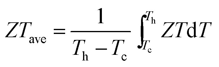 (where Th and Tc are the temperature at the hot-side and cold-side, respectively20). In the temperature range of 373–1073 K, the ZTave of the micro/nano-structured x = 0.02 bulk was ca. 0.13 – again, higher than that of the nano-structured bulks (Fig. 1b), suggesting that a higher TE conversion efficiency was achieved in the micro/nano structured x = 0.02 bulk.
 | ||
| Fig. 1 Temperature dependence of the ZT value (a), thermal conductivity (c), electrical conductivity (d), Seebeck coefficient (e), and power factor (f) for Zn1−xAlxO (x = 0.01, 0.02, 0.03, 0.04 mol) bulks. Note: image (b) is ZTave in the temperature range of 373–1073 K. The data of nano-structured bulks from the ref. 11–13 are given for comparison. | ||
Any improvement in ZTave value relies on a simultaneous enhancement of several TE parameters. The thermal conductivity (κ) shown in Fig. 1c for all the micro/nano-structured bulks continuously decreased over the measuring temperature range, indicating a dominant phonon scattering mechanism. In addition, κ decreased with x down to 1.6 W m−1 K−1 at its lowest point in the micro/nano-structured x = 0.04 bulk at 1073 K. At the same x = 0.02 composition, the micro/nano-structured bulk showed a lower κ value (2.1 W m−1 K−1) than its counterparts at 1073 K, comparable to 1.9 W m−1 K−1 (ref. 12) and 3.2 W m−1 K−1 (ref. 13) in the nano-structured bulk samples; this indicates that low phonon conduction was also effectively retained in the micro/nano-structured bulk due to extremely effective scattering on boundaries and interfaces (which likely were present in the nano-structured bulks).
In regards to electrical transport properties, we observed an outstanding σ value of 1270 S cm−1 in the micro/nano-structured x = 0.02 bulk at room temperature (Fig. 1d) – far higher than the σ value of 50–200 S cm−1 in the nano-structured bulks. The negative Seebeck coefficient (α) shown in Fig. 1e indicated that all samples are n-type semiconductors regardless of the differences in microstructure among them. The |α| values of 45.5–59.8 μV K−1 were obtained at room temperature in the micro/nano-structured bulks, they are comparable to the |α| of ca. 50 μV K−1 for the nano-structured counterparts. The outstanding σ value combined with the comparable |α| value contributed to the final enhanced power factor (PF) shown in Fig. 1f: the highest PF value, 7.2 × 10⁻⁴ W m−1 K−2, was obtained at 1073 K in the micro/nano-structured x = 0.02 bulk and was far higher than that of any nano-structured bulk (especially at the low and medium temperatures).
These results altogether indicate that we did indeed synergistically optimize both the electrical and thermal transport properties in our micro/nano-structured bulk samples. Low phonon conduction can be successfully achieved by ensuring effective scattering from the highly dense grain boundaries and interfaces, though as mentioned in the Introduction, it is very challenging to maintain favorable electrical transport properties. The unique phenomenon we observed in our samples, especially in regards to their electrical transport properties, will be discussed as related to the novel micro/nano-structure in greater detail below.
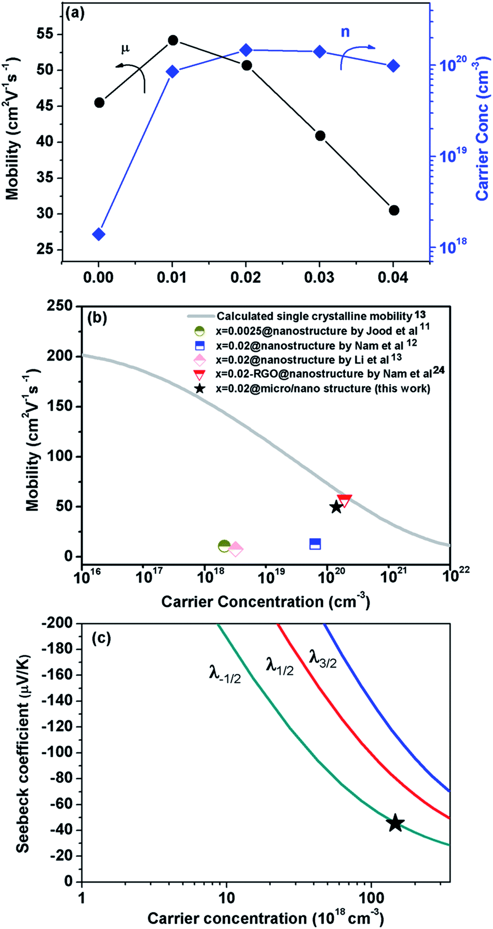
Because σ value is expressed by σ = neμ, (where n and μ are the carrier concentration and the carrier mobility, respectively) the outstanding σ we observed in our micro/nano-structured bulks is attributable to high n and μ values. The Hall measurement results shown in Fig. 2a indicated that the n value increased dramatically from 1.4 × 1018 cm−3 to 8.5 × 1019 cm−3 and 1.5 × 1020 cm−3, as x = 0 increased to x = 0.01 and x = 0.02. This occurred mainly due to the formation of point-defects such as  and/or
  following the reactions
  and
and  . The former interstitial solution of Al3+ enlarged the ZnO lattice, while the latter substitution solution of Al3+ for Zn2+ shrank the lattice due to the smaller ion radius (0.49 Å) of Al3+ compared to Zn2+ (0.74 Å).17
 | ||
| Fig. 2 (a) Carrier concentration (n) and carrier mobility (μ) at room temperature in micro/nano-structured Zn1−xAlxO (x = 0.01, 0.02, 0.03, 0.04 mol) bulks; (b) relationship between n and μ at room temperature for micro/nano structured x = 0.02 bulk, in which the data of ZnO single crystal calculated based on BHD model24 by a gray line and nanostructured Zn1−xAlxO without11–13 and with RGO24 are given for comparison; (c) relationship between Seebeck coefficient and n for micro/nano structured x = 0.02 bulk, with three lines calculated according to λ = 1/2, 3/2, and −1/2 denotes electron scattering from optical phonons, ionized impurities, and acoustic phonons, respectively. | ||
The lattice parameters (a = b = 3.259 Å, c = 5.217 Å) of our x = 0.02 bulk sample were almost unchanged compared to the parameters (a = b = 3.260 Å, c = 5.215 Å) of the x = 0 bulk, which may be ascribed to the fact that  and
and  co-existed in the x = 0.02 bulk; the influence of the former on the lattice parameters offset those of the latter. As x increased to 0.03 and 0.04, n value decreased slightly but stayed around ca. 1 × 1020 cm−3, suggesting that the Al3+ solution in the ZnO neared saturation as x reached 0.02.10 The μ value also increased from 45.5 cm2 V−1 s−1 to 54.2 cm2 V−1 s−1 as x = 0 increased to 0.01, apart from a slight decrease in μ value to 50.7 cm2 V−1 s−1, 40.9 cm2 V−1 s−1 and 30.5 cm2 V−1 s−1 at x = 0.02, x = 0.03 and x = 0.04, respectively. Generally, the μ should decrease after doping Al3+, according to reason that the high n value especially in the high level of n ≥1020 cm−3 increases significantly due to ionized impurity scattering.21 The secondary ZnAl2O4 usually appears as x ≥0.02 and forms a large amount of ZnO/ZnAl2O4 interfaces, which should also increase electron scattering and decrease μ value.11 Regardless of the high n value (up to 8.5 × 1019 cm−3) we observed an unexpected increase in μ at x = 0.01 and a subsequent decrease; these phenomena attributed to x are likely related to the novel micro/nano-structure, which will be discussed in detail later in this paper.
The relationship between n and μ at room-temperature for micro/nano structured x = 0.02 bulk and nanostructured Zn1−xAlxO bulks without11–13 and with RGO24 is plotted in Fig. 2b. The micro/nano-structured x = 0.02 bulk showed higher n and μ values than the nanostructured bulks,11–13 indicating that either high solid solubility of Al3+ or fast electron transport was realized in the micro/nano-structured x = 0.02 bulk. The single crystalline ZnO is known to have excellent electron transport behavior due to the lack of boundaries and interfaces, whose mobility values are calculated based on Matthiessen's rule and BHD model22,23 and plotted in Fig. 2b by a gray line as a function of n value.24 In a recent study, Nam et al. reported that the introduction of reduced graphene oxide (RGO) into nano-structured x = 0.02 bulk can change the electron transport behavior from nanocrystalline to single crystalline.24 When the electrons move across the grain boundaries as freely as they are in the single crystalline ZnO, the μ value is not significantly affected by the grain boundaries due to the reduced or eliminated Schottky barriers. Adding 1 wt% RGO contributed here to relatively high μ value, 57.0 cm2 V−1 s−1, in nano-structured x = 0.02 bulk; this is quite compatible with single crystalline ZnO.24 Interestingly, the micro/nano-structured x = 0.02 bulk without RGO also featured a high μ value (50.7 cm2 V−1 s−1), indicating that similar electron transport behavior to that of single crystalline ZnO was achieved in the micro/nano-structured x = 0.02 bulk as well.
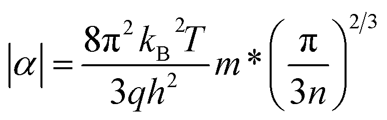
We utilized eqn (1)–(4) to assess the carrier scattering mechanisms. According to the Pisarenko relation for degenerated semiconductors,
 | (1) |
 | (2) |
 | (3) |
 | (4) |
The novel micro/nano-structured characteristics of x = 0.02 bulk are depicted in Fig. 3 via the FESEM and HRTEM observations. An abundance of smooth micro-spheres ca. 3 μm in diameter were observed in the FESEM micrograph as shown in Fig. 3a; this manner of surface morphology indicates that they are dense aggregates composed of nanograins ca. 200 nm in size. This novel structure, the so-called “micro/nano-structure” to which we refer in this paper, is dependent on the original structure in the corresponding powders shown in Fig. 3b where the nanograins are oriented orderly along the axial direction of the micro-spheres due to the spherical restrictions.
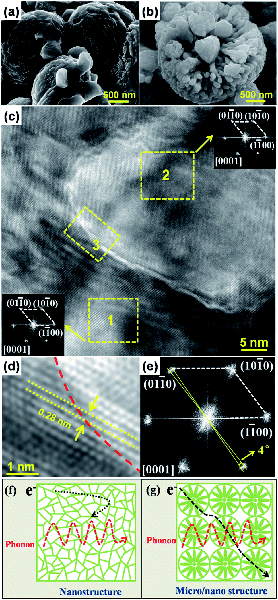 | ||
| Fig. 3 (a and b) FESEM micrograph of micro/nano structured x = 0.02 bulk (a) and powder (b); (c) HRTEM image and its FFT ED diffractogram of selected regions (1, 2) marked with yellow line in micro/nano-structured x = 0.02 bulk; (d) enlarged HRTEM image of selected region 3 from (c) and FFT ED diffractogram (e), in which the angle between two yellow lines represents degree of misorientation between the two nanograins; structural characteristics of the nanostructure (f) and micro/nano-structure (g). | ||
We performed HRTEM and fast Fourier transformation electric diffraction (FFT ED) analyses to examine the misorientation degree among the oriented nanograins in the micro/nano-structured x = 0.02 bulk. According to the FFT ED diffractograms (acquired from the yellow regions 1 and 2) shown in Fig. 3c, each nanograin exhibited a nearly identical [0001] zone-axis pattern. There also was similar lattice spacing of 0.28 nm corresponding to the distance between the (10![[1 with combining macron]](https://www.rsc.org/images/entities/char_0031_0304.gif) 0) lattice planes of ZnO. The HRTEM image shown in Fig. 3d also indicated clear, uniform stripes (acquired from the yellow region 3) even across the grain boundaries (described by the red lines) among the nanograins. The corresponding FFT ED diffractogram shown in Fig. 3e further confirmed that all nanograins in region 3 exhibited practically identical [0001] zone-axis patterns with misorientation degree of about ca. 4°; in effect, a nearly coherent grain boundary was successfully obtained.
0) lattice planes of ZnO. The HRTEM image shown in Fig. 3d also indicated clear, uniform stripes (acquired from the yellow region 3) even across the grain boundaries (described by the red lines) among the nanograins. The corresponding FFT ED diffractogram shown in Fig. 3e further confirmed that all nanograins in region 3 exhibited practically identical [0001] zone-axis patterns with misorientation degree of about ca. 4°; in effect, a nearly coherent grain boundary was successfully obtained.
We speculated that the misorientation degree would decreased as the diameter of rod-like and spheroidal particles in the micro-spheres decreased; to this effect, we assumed that refining the grain sizes would enhance the degree of coherence between grain boundaries and thus the rapid transfer of electrons. This novel micro/nano structure characteristic is similar to the mosaic structure characteristic obtained in Cu2 (S, Te) polycrystalline bulks prepared via flash cooling.26 Said mosaic structure characteristic functions similarly to quasi-single crystals composed of nanograins with identical (or nearly identical) orientation as electrons are freely transferred along the frames of quasi-single crystals.26 Hence, the nearly coherent grain boundary among the nanograins for the micro/nano-structures likely dominated the electron transport behavior (again, like single crystalline ZnO) in the x = 0.02 bulk sample (Fig. 2b).
We further explored the electron transport behavior in our samples by comparison among them, as depicted in Fig. 3f and g. As opposed to the nanostructure in which nanograins are oriented completely randomly and their misaligned interfaces affect electron transfer (black arrow in Fig. 3f), nanograins in the novel micro/nano-structure were orderly oriented along the axial direction of micro-spheres due to the spherical restrictions (Fig. 3g), as discussed above; again, this seemed conducive to obtaining the nearly coherent nanograin boundaries which facilitate a fast path for electron transport. The conjoined micro-spheres in the micro/nano-structure also created a coherent crystalline framework for the less-affected electron transport (black arrow in Fig. 3g). In regards to phonon transport, the nano-structure and micro/nano-structure were expected to feature analogous behavior based on the fact that a phonon does not select its own transport path (red arrows in Fig. 3f and g).
These observations altogether again confirm that a novel micro/nano microstructure was successfully obtained in the x = 0.02 bulk sample in which nanograins with nearly coherent grain boundaries not only provided a favorable crystalline framework for rapid electron transfer, but also effectively scattered phonons. This allowed us to synergistically optimize both electrical and thermal transport properties, as depicted in Fig. 1, in the x = 0.02 micro/nano-structured bulk sample; we achieved “phonon-glass electron-crystal” characteristics in our sample, a classic thermoelectric concept.27
Shape-controlled synthesis of micro/nano-structured ZnO-based powders
The formation of the novel micro/nano-structure in bulk materials depends on the original micro/nano-structure in the corresponding powders, as the precursor powder microstructure is easily retained or frozen in the sintered body during (brief, low-temperature) SPS. We used triethanolamine (TEA) as a surfactant in preparing the precursor powder via HS. The function of this material on the precursor powder morphology is schematically proposed in Fig. 4. As shown in Fig. 4a, TEA was initially dissociated in water to provide a basic alkalescent environment (eqn (1)) to form a Zn(OH)2 precipitate complex (eqn (2)) which favors the anisotropic growth of ZnO.16,17 Along with TEA chelation, it also coordinated with [Zn(OH)2]n to form a complex [Zn(OH)2TEA]n (eqn (3)) which transformed into ZnO·nTEA nuclei during the HS process (eqn (4)). The corresponding nucleation process is schematically shown in Fig. 4b. During the growth process, wurtzite-structured ZnO tends to take anisotropic growth along the [0001] direction under OH− rich conditions with NH3·H2O; OH− united with Zn2+ forms the growth unit [Zn(OH)4]2− dominating the anisotropic growth of ZnO.16,17 In our experiment, the anisotropic growth of ZnO particles proceeded under the dominant eqn (1) as TEA content was relatively low (Fig. 4c). With moderate TEA content, some TEA molecules that did not participate in eqn (1) were absorbed on the surface of ZnO particles and limited their anisotropic growth to some extent. With high TEA content, the ZnO particles did not readily refine as their sizes reached the nanoscale, because the TEA absorbed around ZnO particles and became saturated; at this point, aggregation began to accelerated due to TEA chelation because the abundant hydroxyl groups of the TEA rims absorbed on ZnO nanoparticles interacted with each other. This resulted in linkage or a bridging of the neighboring ZnO nanoparticles.28 The ZnO nanoparticles also aggregated ultimately into micro-spheres along the axial direction, reducing the surface Gibbs free energy of the system. In short, the orientation of nanoparticles should be spherically restricted rather than randomly self-assembled.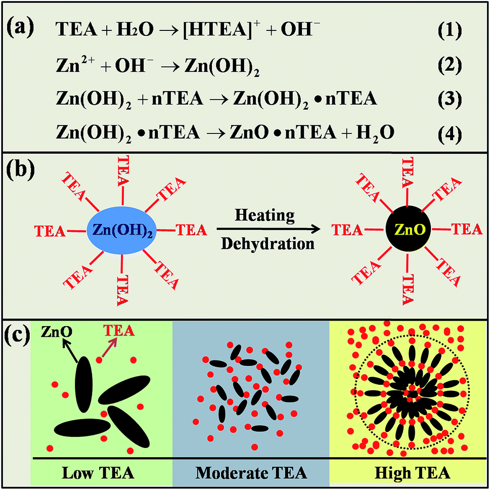 | ||
| Fig. 4 Function of TEA on preparing micro/nano powders during HS process including reaction equations (a); nucleation (b); growth (c). | ||
The FESEM micrographs of ZnO powders with various TEA contents shown in Fig. 5a–e support the above description. At TEA content of 5 ml (Fig. 5a), the sample consisted of a single or a twined ZnO with bullet-like morphology, average length of ca. 6 μm, and mean diameter of ca. 4 μm (the aspect ratio is ca. 1.5), indicating the persistence of anisotropic growth. Well-resolved hexagonal edges and corners were also observed, indicating favorable crystalline ZnO quality. As TEA content increased to 10 ml (Fig. 5b), mushroom-like ZnO particles with cusped ends formed with a decreased average length of ca. 4 μm and mean diameter of ca. 2 μm (aspect ratio = ca. 2), indicating that the TEA as surface modifier suppressed growth both in length and in diameter.
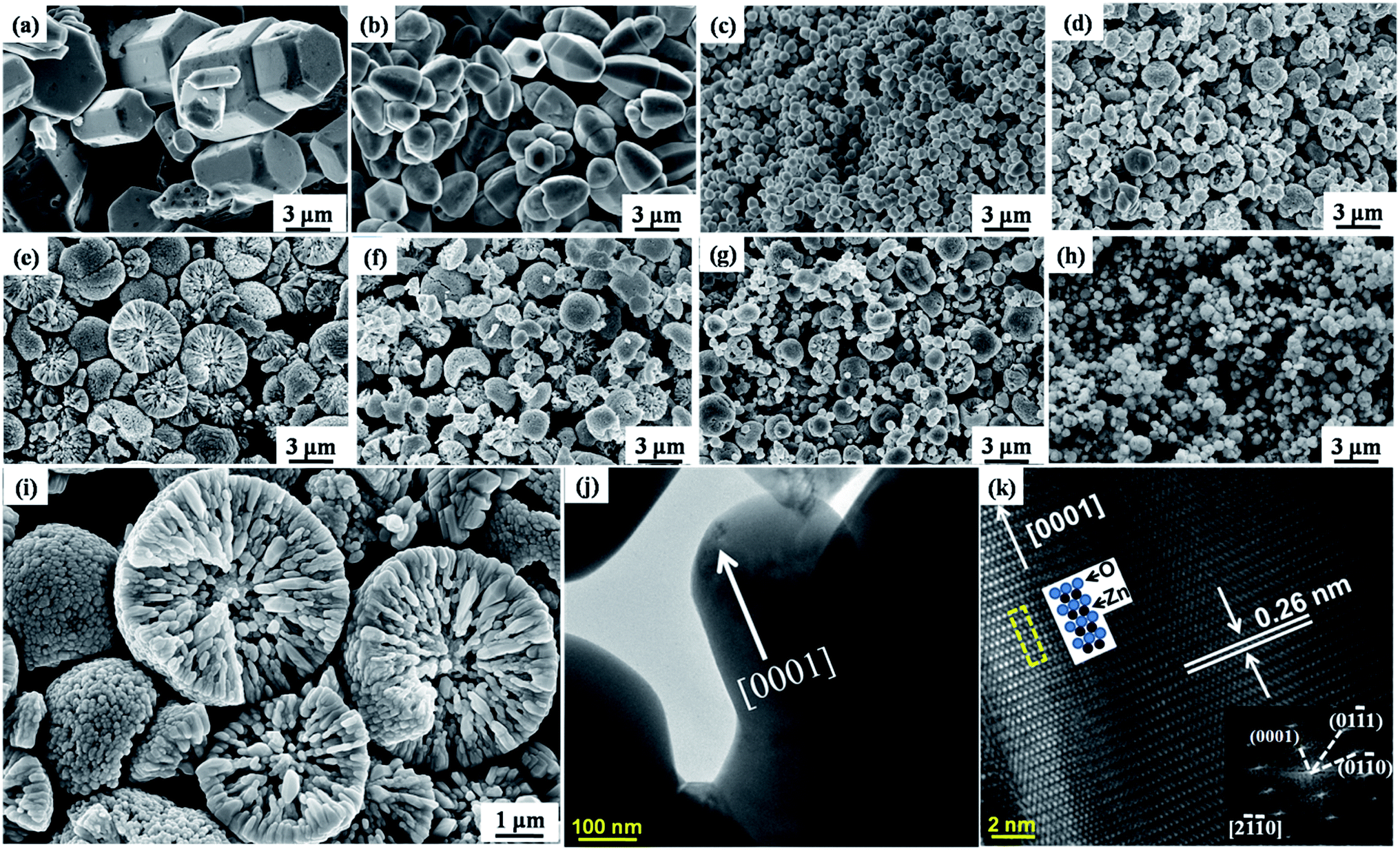 | ||
| Fig. 5 FESEM micrographs of Al-free ZnO with TEA of 5 ml (a), 10 ml (b), 20 ml (c), 25 ml (d), 30 ml (e and i) and Zn1−xAlxO using fixed TEA of 30 ml at x = 0.01 (f), x = 0.02 (g), x = 0.04 (h); TEM image (j); HRTEM image (k); inserted FFT diffractogram for the Al-free ZnO shown in (i). | ||
Similar inhibition in ZnO growth has been reported by previous researchers using TEA as a surface modifier.29 Others have also confirmed a joint behavior along the radial plane of mushroom-like ZnO particles resulting from the linkage behavior caused by TEA.29 By further increasing TEA to 20 ml (Fig. 5c), spheroidal particles emerged with a decreased average grain size to ca. 600 nm. Interestingly, most spheroidal particles began to aggregate to micro-spheres with an average size of ca. 2 μm as TEA increased to 25 ml (Fig. 5d). This aggregative behavior was further enhanced by increasing TEA to 30 ml, at which point a large amount of micro-spheres ca. 5 μm in size were obtained (Fig. 5e); a magnified FESEM image of these particles is shown in Fig. 5i. The micro-spheres in this sample were loose and oriented along the axial direction by rod-like particles 100–600 nm in size and spheroidal nanoparticles 50–100 nm in size. The formation of this novel micro/nano-structure relates to a non-classical crystallization mechanism called “oriented aggregation” which yields multiform crystal structures and morphologies.30
Analogical self-assembly structures were also reported in α-Fe2O3 particles by Sugimoto et al.31 The rod-like particles in micro/nano-structured ZnO powders (Fig. 5j) were around ca. 300 nm in diameter, which is consistent with the FESEM observation shown in Fig. 5i. The corresponding HRTEM analysis shown in Fig. 5k indicated that lattice spacing of 0.26 nm for the rod-like ZnO corresponded to the (0002) planes of the wurtzite-structured ZnO.28 The fast Fourier transform (FFT) of the diffractogram (bottom, right corner) showed a single crystal-type [20] zone-axis pattern. These results indicate that the growth direction of our highly crystalline ZnO rod-like particles was consistent with the crystallographic [0001], similar to the anisotropic growth of ZnO during HS.32
Interestingly, the formation of this novel micro/nano-structure was hindered by adding Al as evidenced by the x-evolved morphology (Fig. 5f–h) when the TEA content was fixed to 30 ml. After doping Al to x = 0.01, the loose micro/nano-structured powders shown in Fig. 5f decreased to ca. 3 μm in micro-sphere diameter, to ca. 300 nm in rod-like particle size, and to ca. 40 nm in spheroidal particle size. This may have been because Al3+ acted as a competitive ligand of Zn2+ united with OH− to form Al(OH)3 prior [Zn(OH)4]2−, which decreased the amount of [Zn(OH)4]2− dominating the anisotropic growth during the HS process.16,17 As x increased to 0.02 and 0.04 (Fig. 5g and h), the sizes in particles and micro-spheres of micro/nano-structured powders further decreased. These results indicate that doping Al in the micro/nano-structured ZnO powders refined both the particles11 and the micro-spheres.
Phase and orientation of micro/nano-structured ZnO-based bulks
The micro/nano-structure of precursor powders shown in Fig. 6a–d (enlarged in Fig. 6e–h) was clearly well-frozen in their corresponding bulks by applying SPS. The sizes of both micro-spheres and matrix grains also decreased as x increased corresponding to the behavior of the precursor powders. Compared with the x = 0 and x = 0.01 bulks shown in Fig. 6a, b, e and f, many white nanoprecipitates about ca. 10 nm in size were observed in the micro/nano-structured x = 0.02 bulk in Fig. 6c and g, i.e., 10 to 20 times smaller than that of nano-structured bulks synthesized by Jood et al.11 and Nam et al.12 The white nanoprecipitates increased in quantity and average size to ca. 30 nm as x increased to 0.04 in Fig. 6d and h. The EDX line analyses and atomic number contrast images (Fig. 6i) indicated that the new nanoprecipitates in Fig. 6g and h were rich in Al and O, corroborating the formation of ZnAl2O4. In addition to the different morphologies, the relative density of the micro/nano-structured bulks were 84%, 82%, 80%, 76%, and 72% as x = 0, 0.01, 0.02, 0.03, and 0.04, respectively, corresponding to increased quantities of pores. Overall, the refined matrix grains, ZnAl2O4 nanoprecipitates, and pores dominated the strong phonon scattering and contributes to the lower k shown in Fig. 1c.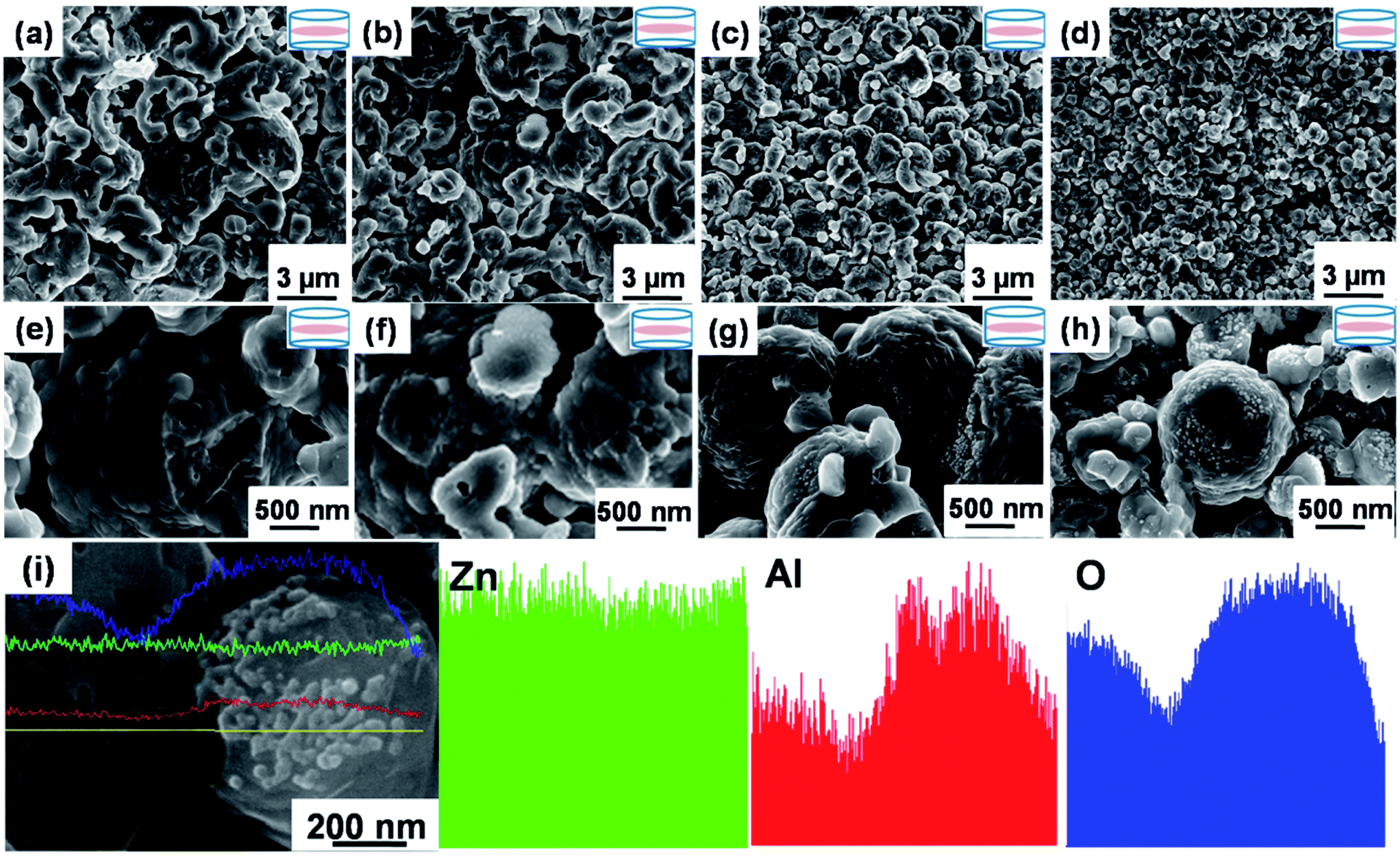 | ||
| Fig. 6 FESEM micrographs of micro/nano-structured Zn1−xAlxO bulks with x = 0 (a and e), 0.01 (b and f), 0.02 (c and g) and 0.04 (d and h); representative EDX line scans of O, Zn, and Al Kα1 X-ray peaks obtained across ZnAl2O4 nanoprecipitates along yellow line in the FESEM micrograph (i) magnified from image (h). | ||
The phase structures of micro/nano-structured powders and bulks were compared as shown in Fig. 7a and b. The corresponding diffraction are well matched to those of wurtzite-structured ZnO (PDF#36-1451). The secondary ZnAl2O4 impurity observed by FESEM micrographs in Fig. 6g and h was un-detected by XRD even as x = 0.04, as their content was below the detection limit of the XRD analysis method. ZnAl2O4 impurity is typically detected by XRD in bulks sintered by solid state reaction (SSR), for example, in air at 1673 K for 10 h with 2% mol Al doping;10 but may be undetectable in the counterpart sintered by SPS below 1223 K for less than 10 min in a vacuum.12,33 We therefore speculated that the short sintering time (only 5 min) and low sintering temperature (below 1223 K) of SPS did not effectively facilitate the formation of ZnAl2O4.
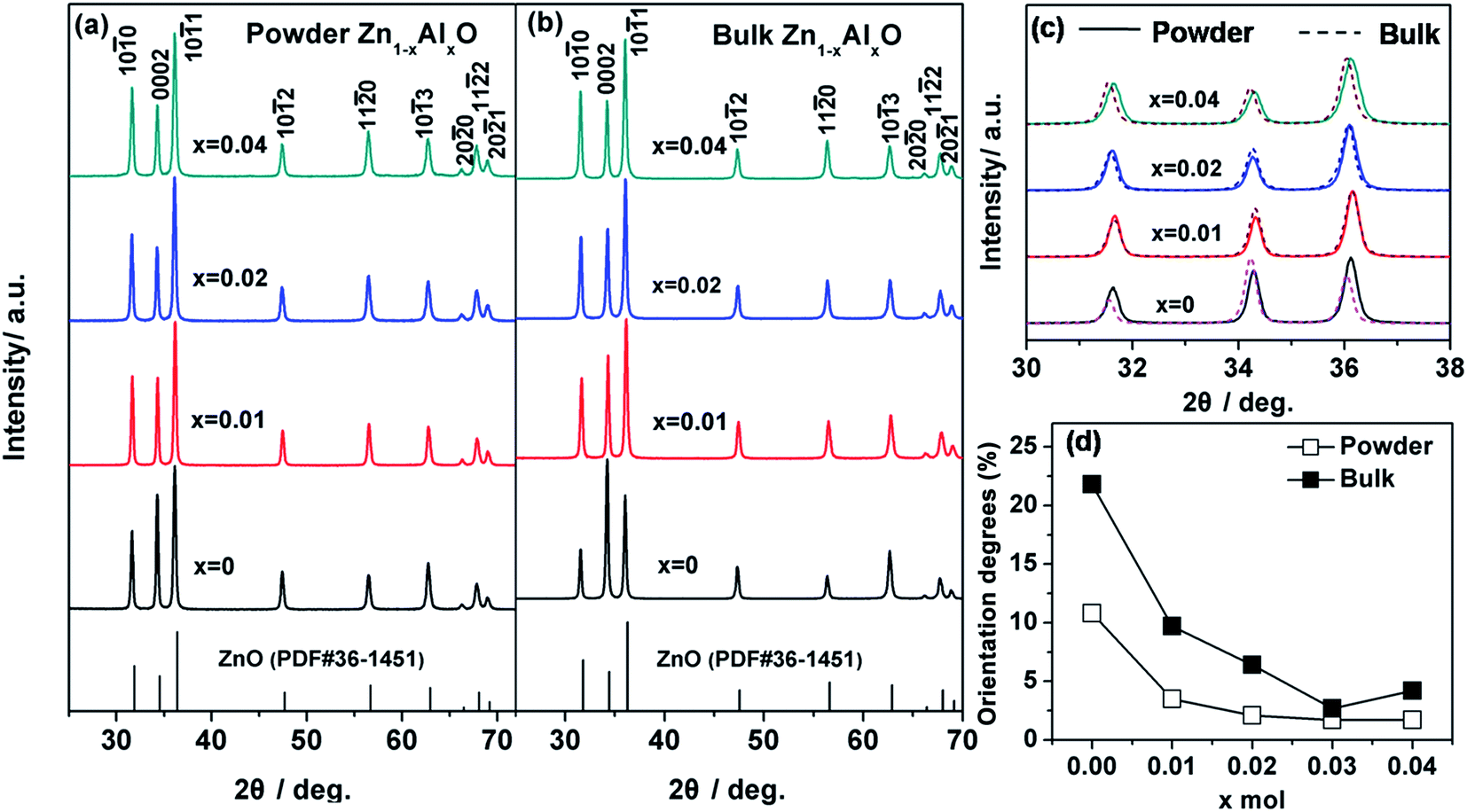 | ||
| Fig. 7 XRD patterns in 25–70° of Zn1−xAlxO (x = 0, 0.01, 0.02, 0.04) powders (a) and bulks (b) with respective XRD patterns in 30–38° (c) and their corresponding texturing degrees (d). | ||
The high solid solubility of Al contributing to the high n (Fig. 2b) also contributed to the decreased formation ZnAl2O4. We did not observe any obvious trend in the main diffraction peaks in our bulks as compared to that of the powders shown in Fig. 7c, indicating delayed grain growth during the SPS process. This is also evidence that the micro/nano-structure of precursor powders was frozen perfectly in their corresponding bulks. Apart from the identical phase structure between powders and bulks, it is noted in Fig. 7a and b that the intensity of the (0002) diffraction peak differed as x differed; this indicated a varied orientation caused by x and the SPS process.
Fig. 7d shows the orientation degree F(000l) calculated by the Lotgering method34 for both powders and bulks as a function of x. The F(000l) value is 10.8% for the micro/nano structured x = 0 powder, which can be ascribed to the formation and growth of rod-like powders along the [0001] direction and the axially restriction by micro-spheres (Fig. 5i). This micro/nano-structural characteristic weakened as x increased (Fig. 5e–h), which reflects the decreased F(000l) value to 3.5%, 2.1%, 1.7%, and 1.7% at x = 0.01, x = 0.02, 0.03, and 0.04. Compared to their corresponding powders, all bulks showed increased F(000l) values to 21.8%, 6.4%, 9.7%, 2.7%, and 4.2% as x = 0, 0.01, 0.02, 0.03, and 0.04, respectively, indicating that the F(000l) orientation in the powder was further enhanced in the corresponding bulk under applied pressure.
ZnO15,16,35 and Bi2S3 36 bulks have been reported to be preferentially oriented in the (hki0) plane perpendicular (⊥) to the pressure direction when rod-like powders grown preferentially at the same [0001] direction are consolidated, as rods readily collapse under applied pressure. Our bulks, which were preferentially oriented in (000l) perpendicular (⊥) to the pressure direction, did not behave this way – we attribute this discrepancy to the micro/nano-structure having slowed the collapse rod-like particles due to spherical restrictions. The decreased F(000l) with x (Fig. 7d) in powders and bulks corresponds to decrease in both the diameter of micro-spheres as well as rod-like and spheroidal particles in the powders (Fig. 5e–h) or bulks (Fig. 6a–h) leading to fewer grain boundaries and less electron scattering. Because higher orientation degree relates to higher μ, we assumed that the increased μ from x = 0 to x = 0.01 bulks (Fig. 2a) contributed predominantly to the reduced decree of misorientation among coherent grain boundaries rather than the F(000l). Ultimately, we concluded that the μ values we obtained in the micro/nano-structured bulks were mainly related to the novel micro/nano-structure itself being conducive to the formation of a nearly coherent crystalline framework for rapid electron transfer.
Conclusions
A unique micro/nano structure was successfully obtained in Zn1−xAlxO (x = 0, 0.02, 0.03, 0.04 mol) bulks prepared via HS and SPS. The nanograins were oriented along the axial direction of micro-spheres with a low misorientation degree between the neighboring grains. Due to the near-coherence of grain boundaries, the micro/nano structured x = 0.02 bulk achieved a remarkably high μ value of 50.7 cm2 V−1 s−1 – close to that of single crystals – as well as a low κ value (2.1 W m−1 K−1) likely arising in the nano-structured bulks due to effective scattering on the boundaries and interfaces. The synergistic optimization of electrical and thermal transport properties led to a high ZT value, 0.36, at 1073 K.The novel micro/nano-structure we established is likely applicable to other TE materials, as well. We also believe that this strategy can work in tandem with other successful TE-enhancement approaches such as modulation doping and band structure engineering.
Acknowledgements
This work was supported by the National Natural Science Foundation of China (grant no. 51272023) and National Basic Research Program of China (grant no. 2013CB632503).References
- D. Kraemer, B. Poudel, H. P. Feng, J. C. Caylor, B. Yu, X. Yan, Y. Ma, X. W. Wang, D. Z. Wang, A. Muto, K. McEnaney, M. Chiesa, Z. F. Ren and G. Chen, Nat. Mater., 2011, 10, 532–538 CrossRef CAS PubMed.
- J. F. Li, W. S. Liu, L. D. Zhao and M. Zhou, NPG Asia Mater., 2010, 2, 152–158 CrossRef.
- M. Zhou, J. F. Li and T. Kita, J. Am. Chem. Soc., 2008, 130, 4527–4532 CrossRef CAS PubMed.
- L. D. Zhao, B. P. Zhang, J. F. Li, M. Zhou, W. S. Liu and J. Liu, J. Alloys Compd., 2008, 455, 259–264 CrossRef CAS.
- J. Elias, M. Bechelany, I. Utke, R. Erni, D. Hosseini, J. Michler and L. Philippe, Nano Energy, 2012, 1, 696–705 CrossRef CAS.
- L. Li, T. Y. Zhai, Y. Bando and D. Golberg, Nano Energy, 2012, 1, 91–106 CrossRef CAS.
- L. Lin, Y. F. Hu, C. Xu, Y. Zhang, R. Zhang, X. N. Wen and Z. L. Wang, Nano Energy, 2013, 2, 75–81 CrossRef CAS.
- G. C. Yoon, K. S. Shin, M. K. Gupta, K. Y. Lee, J. H. Lee, Z. L. Wang and S. W. Kim, Nano Energy, 2015, 12, 547–555 CrossRef CAS.
- M. Ohtaki, T. Tsubota, K. Eguchi and H. Arai, J. Appl. Phys., 1996, 79, 1816 CrossRef CAS.
- T. Tsubota, M. Ohtaki, K. Eguchi and H. Arai, J. Mater. Chem., 1997, 7, 85–90 RSC.
- P. Jood, R. J. Mehta, Y. L. Zhang, G. Peleckis, X. L. Wang, R. W. Siegel, T. Borca-Tasciuc, S. X. Dou and G. Ramanath, Nano Lett., 2011, 11, 4337–4342 CrossRef CAS PubMed.
- W. H. Nam, Y. S. Lim, S. M. Choi, W. S. Seo and J. Y. Lee, J. Mater. Chem., 2012, 22, 14633–14638 RSC.
- L. Han, N. Van Nong, W. Zhang, L. T. Hung, T. Holgate, K. Tashiro, M. Ohtaki, N. Pryds and S. Linderoth, RSC Adv., 2014, 4, 12353–12361 RSC.
- D. S. Chen, Y. Zhao, Y. Chen, B. Wang, H. Y. Chen, J. Zhou and Z. Liang, ACS Appl. Mater. Interfaces, 2015, 7, 3224–3230 CAS.
- T. Sahoo, M. Kim, J. H. Baek, S. R. Jeon, J. S. Kim, Y. T. Yu, C. R. Lee and I. H. Lee, Mater. Res. Bull., 2011, 46, 525–530 CrossRef CAS.
- D. B. Zhang, B. P. Zhang, D. S. Ye and Y. B. Zhu, Ceram. Int., 2015, 41, 14627–14634 CrossRef CAS.
- D. B. Zhang, B. P. Zhang, D. S. Ye, Y. C. Liu and S. Li, J. Alloys Compd., 2016, 656, 784–792 CrossRef CAS.
- H. Zhang, D. Yang, Y. Ji, X. Y. Ma, J. Xu and D. L. Que, J. Phys. Chem. B, 2004, 108, 3955–3958 CrossRef CAS.
- H. Zhang, D. Yang, X. Y. Ma, Y. Ji, J. Xu and D. L. Que, Nanotechnology, 2004, 15, 622–626 CrossRef CAS.
- L. D. Zhao, X. Zhang, H. J. Wu, G. J. Tan, Y. L. Pei, Y. Xiao, C. Chang, D. Wu, H. Chi, L. Zheng, S. K. Gong, C. Uher, J. Q. He and M. G. Kanatzidis, J. Am. Chem. Soc., 2016, 138, 2366–2373 CrossRef CAS PubMed.
- J. G. Lu, Z. Z. Ye, Y. J. Zeng, L. P. Zhu, L. Wang, J. Yuan, B. H. Zhao and Q. L. Liang, J. Appl. Phys., 2006, 100, 73714 CrossRef.
- D. C. Look, D. C. Reynolds, J. R. Sizelove, R. L. Jones, C. W. Litton, G. Cantwell and W. C. Harsch, Solid State Commun., 1998, 105, 399–401 CrossRef CAS.
- K. Ellmer, J. Phys. D: Appl. Phys., 2001, 34, 3097–3108 CrossRef CAS.
- W. H. Nam, B. B. Kim, S. G. Seo, Y. S. Lim, J. Y. Kim, W. S. Seo, W. K. Choi, H. H. Park and J. Y. Lee, Nano Lett., 2014, 14, 5104–5109 CrossRef CAS PubMed.
- F. May and G. J. Snyder, Introduction to Modeling Thermoelectric Transport at High Temperatures, in Thermoelectrics and its Energy Harvesting, ed. D. M. Rowe, CRC Press, Boca Raton, 2012 Search PubMed.
- Y. He, P. Lu, X. Shi, F. F. Xu, T. S. Zhang, G. J. Snyder, C. Uher and L. D. Chen, Adv. Mater., 2015, 27, 3639–3644 CrossRef CAS PubMed.
- C. Xiao, J. Xu, B. X. Cao, K. Li, M. G. Kong and Y. Xie, J. Am. Chem. Soc., 2012, 134, 7971–7977 CrossRef CAS PubMed.
- S. Xu, Z. H. Li, Q. Wang, L. J. Cao, T. M. He and G. T. Zou, J. Alloys Compd., 2008, 465, 56–60 CrossRef CAS.
- R. G. Xie, D. S. Li, H. Zhang, D. R. Yang, M. H. Jiang, T. Sekiguchi, B. D. Liu and Y. S. Bando, J. Phys. Chem. B, 2006, 110, 19147–19153 CrossRef CAS PubMed.
- T. He, D. R. Chen, X. L. Jiao, Y. Y. Xu and Y. X. Gu, Langmuir, 2004, 20, 8404–8408 CrossRef CAS PubMed.
- T. Sugimoto, Y. S. Wang, H. Itoh and A. Muramatsu, Colloids Surf., A, 1998, 134, 265–279 CrossRef CAS.
- B. Cheng and E. T. Samulski, Chem. Commun., 2004, 8, 986 RSC.
- K. H. Kim, S. H. Shim, K. B. Shim, K. Niihara and J. Hojo, J. Am. Ceram. Soc., 2005, 88, 628–632 CrossRef CAS.
- T. Tani, S. Isobe, W. S. Seo and K. Koumoto, J. Mater. Chem., 2001, 11, 2324–2328 RSC.
- J. L. Ning, D. M. Jiang, K. H. Kim and K. B. Shim, Ceram. Int., 2007, 33, 107–114 CrossRef CAS.
- Z. H. Ge, B. P. Zhang, P. P. Shang and J. F. Li, J. Mater. Chem., 2011, 21, 9194–9200 RSC.
| This journal is © The Royal Society of Chemistry 2017 |