
 Open Access Article
 This Open Access Article is licensed under a Creative Commons Attribution-Non Commercial 3.0 Unported Licence
Direct and self-selective synthesis of Ag nanowires on patterned graphene†
Tran Nam Trung ,
Dong-Ok Kim and
Eui-Tae Kim*
,
Dong-Ok Kim and
Eui-Tae Kim*
Department of Materials Science & Engineering, Chungnam National University, Daejeon 305-764, Korea. E-mail: etkim@cnu.ac.kr
First published on 20th March 2017
Abstract
We report the direct and self-selective synthesis of Ag nanowires (NWs) on graphene patterns through a modified citrate reduction reaction approach. High-density NWs were selectively formed only on the graphene areas, whereas NWs were not synthesized on the SiO2/Si and glass substrates. The size and density of the Ag NWs gradually increased with increasing reaction time and AgNO3 concentration. When the Ag NWs were synthesized with 60 mM AgNO3 at 90 °C for 30 min, the average width and length of the NWs were approximately 150 nm and 3 μm, respectively. Graphene–Ag NW hybrids showed excellent light transmittance (91.5% at 550 nm) with low sheet resistance (102 Ω sq−1). These properties can be further optimized by manipulating the size and density of the Ag NWs. This simple and cost-effective process for the fabrication of graphene–Ag NW hybrid electrode patterns is useful for a variety of applications.
Introduction
The composites of metals with one- and two-dimensional carbon nanostructures have been extensively studied for promising applications, such as transparent electrodes, catalysts, and supercapacitors.1–5 In particular, graphene–metal hybrid structures have recently attracted considerable attention for use as flexible transparent electrodes in various device applications such as displays, solar cells and light emitting diodes (LEDs).6–8 Commercial indium–tin-oxide electrode could be replaced by graphene that possesses several very valuable attributes: an extremely high charge carrier mobility of ∼200![[thin space (1/6-em)]](https://www.rsc.org/images/entities/char_2009.gif) 000 cm2 V−1 s−1; a low intrinsic sheet resistance of ∼30 Ω sq−1; and a high visible-light transmittance up to 97.5%.8,9 However, large-area graphene layers that are prepared on metals via chemical vapor deposition (CVD) and are then transferred to desired substrates have shown detrimental carrier transport properties due to carrier scattering by defects such as dislocations, grain boundaries, folds, and cracks.10 Such a relatively low level of electrical conductivity can be significantly enhanced by utilizing metal nanowires (NWs) providing ideal one-dimensional charge transport pathways. Recent theoretical calculation has shown that even sub-percolating metal NWs and nanotubes can be very effective electrical conductance routes on polycrystalline graphene.11 Kholmanov et al.10 experimentally achieved a sheet resistance of 64 Ω sq−1 for graphene–Ag NW hybrid films, whereas a sheet resistance of the counterpart graphene was approximately 1 kΩ sq−1. Lee et al.8 recently reported a flexible graphene–Ag NW electrode with a low sheet resistance of 33 Ω sq−1 and high visible-light transmittance of 94%.
000 cm2 V−1 s−1; a low intrinsic sheet resistance of ∼30 Ω sq−1; and a high visible-light transmittance up to 97.5%.8,9 However, large-area graphene layers that are prepared on metals via chemical vapor deposition (CVD) and are then transferred to desired substrates have shown detrimental carrier transport properties due to carrier scattering by defects such as dislocations, grain boundaries, folds, and cracks.10 Such a relatively low level of electrical conductivity can be significantly enhanced by utilizing metal nanowires (NWs) providing ideal one-dimensional charge transport pathways. Recent theoretical calculation has shown that even sub-percolating metal NWs and nanotubes can be very effective electrical conductance routes on polycrystalline graphene.11 Kholmanov et al.10 experimentally achieved a sheet resistance of 64 Ω sq−1 for graphene–Ag NW hybrid films, whereas a sheet resistance of the counterpart graphene was approximately 1 kΩ sq−1. Lee et al.8 recently reported a flexible graphene–Ag NW electrode with a low sheet resistance of 33 Ω sq−1 and high visible-light transmittance of 94%.
Many methods have been developed to produce graphene–Ag NW hybrids: drop and spin coating, spray casting, Meyer rod casting, and transferring methods.12–14 Those methods, however, possess complexities of fabrication processing that are based on the mechanical assembly of separately pre-synthesized Ag NWs and a graphene matrix. Moreover, the mechanical assembly can inherently result in poor adhesion properties at the NWs–NWs and NWs–graphene junctions, causing high contact resistance and mechanical failure. To solve those problems, further complicate graphene–Ag NWs–graphene sandwich structures and welding and soldering processes at the inter-NW junctions have been studied.15,16 A simple and reliable fabrication method could result from the direct growth of Ag NWs on graphene. Despite extensive study on NWs synthesis via vapor-phase deposition and wet-chemistry approaches, the direct growth of metal NWs on graphene has yet to be reported.
Another important aspect of electrode applications is patterning for a variety of device applications. However, the patterning of graphene–metal NW hybrid films by dry and wet etching is a multi-step and time-consuming task due to the usage of two different adequate plasma gas chemistries and wet etchants for graphene and metal. Although Ag NWs can be selectively casted onto graphene via mechanical-assembly approaches with the assistance of pre-patterned templates such as photoresist, the poor adhesion of Ag NWs and graphene is problematic during the process of removing the templates, which results in only the production of significantly wide-patterned electrodes.
In the present study, we report the direct synthesis of Ag NWs on graphene by employing a concept of electroless deposition in a modified citrate reduction solution. Moreover, our synthesis method produces the self-selective growth of Ag NWs only on pre-patterned graphene areas on SiO2/Si and glass substrates, which provides various electrode patterns in an easy and low-cost manner. Electroless deposition is considered a promising method for the selective growth of metal films on seed layer patterns. There also have been several reports on the electroless deposition of Ag nanoparticles (NPs) and film coating on graphene and carbon nanotubes. However, those methods were mostly based on a surface-catalyzed growth mechanism, which results from functional groups and catalytic metal NPs such as Pd and Ni deposited onto otherwise inert surfaces.17,18 Meanwhile, a citrate reduction reaction was recently introduced to form Ag NPs on graphene with no catalytic metal decoration on the surface. The method offers a mild condition in order to minimize damage to that graphene, which includes the use of a low reaction temperature below 100 °C. Owing to the characteristic weak binding of citrate to the core Ag, a stabilizing agent such as poly-vinylpyrrolidone (PVP) is usually used to enhance the dispersion of Ag colloids. PVP prevents the associated agglomeration of Ag colloids; as a result, only NPs are produced.19–21 In our study, we eliminated the use of any stabilizing agents in order to induce the growth of NW structures rather than NPs.
Results and discussion
High-quality graphene was synthesized on Cu foil using inductively-coupled plasma chemical vapor deposition (ICP CVD). The graphene on the Cu foil was subsequently transferred onto SiO2/Si and glass substrates. Grid patterns of graphene were prepared on substrates by using photolithography and plasma etching, as shown in the insets of Fig. 1(a) and (b). The removal of graphene was confirmed by optical microscopy and Raman spectroscopy. The graphene area showed the typical Raman spectrum of a high-quality pristine graphene with a D to G peak intensity ratio of 0.13 (see ESI, Fig. S1(a)†). High-resolution transmission electron microscopy (HRTEM) study revealed that the graphene film consisted of mainly monolayer and bilayer graphenes (see ESI, Fig. S1(b)†). The HRTEM analysis agreed well with the Raman spectrum, which showed a very small value (<30 cm−1) of the full width at half maximum (FWHM) of the 2D band. Ag NWs were synthesized using 60 mM AgNO3 at 90 °C on the patterns. Na3C6H5O7 was used as a reducing agent. For a 30 min reaction, high-density NWs were selectively formed only on the graphene areas, whereas NWs were not synthesized on the SiO2/Si substrates. The NWs were densely grown and well-connected on narrow (20 μm in width, referred to here as pattern A) and wide graphene areas (200 μm in width, referred to here as pattern B) of grid patterns, as shown in Fig. 1(a) and (b), respectively. The average width and length of the NWs were approximately 150 nm and 3 μm, respectively (Fig. 1(c)).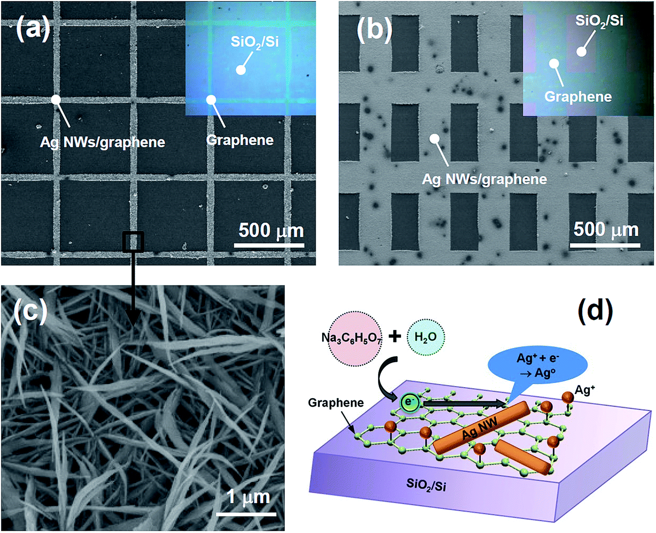 | ||
| Fig. 1 SEM images of Ag NWs synthesized on pre-patterned graphene: (a) pattern A, (b) pattern B, and (c) enlarged Ag NW image. The insets show the microscope images of graphene patterns on SiO2/Si substrates. (d) Schematic diagram of Ag NWs on graphene synthesized using a modified citrate reduction reaction. | ||
The size and density of the NWs were successfully controlled by the synthesis time and the AgNO3 concentration. Fig. 2 shows the scanning electron microscopy (SEM) images of Ag NWs on graphene synthesized at various reaction times (30 s to 30 min) using a fixed AgNO3 concentration of 30 mM. Sparse NPs and NWs of sub-μm length were observed at 30 s of reaction time, as shown in Fig. 2(a). The density and length of the NWs gradually increased with the reaction time. The average width and length of the NWs synthesized with a reaction time of 10 min were approximately 100 nm and 1 μm, respectively (Fig. 2(c)). At a 30 min reaction, the width and length of the NWs reached approximately 100–150 nm and 2 μm, respectively (Fig. 2(d)). The 2 μm-long NWs were well cross-linked with each other and covered the graphene surface uniformly, as shown in Fig. 3(a). With an increase in AgNO3 concentration to 60 mM, the density and size of the NWs significantly increased (Fig. 3(b)). The average length was approximately 3 μm. However, the NW-like shape was dramatically changed to nanosheets at a very high AgNO3 concentration of 300 mM, as shown in Fig. 3(c).
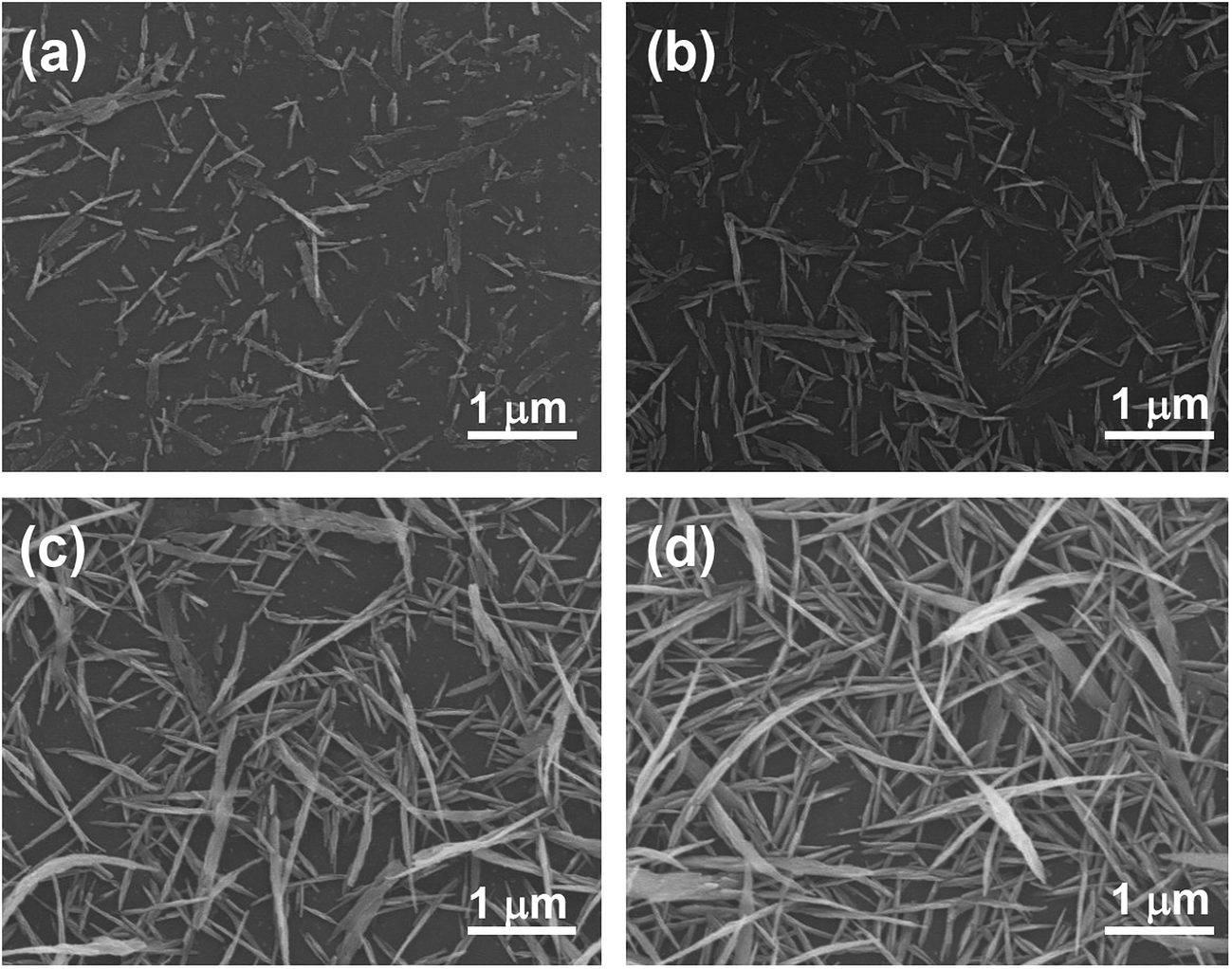 | ||
| Fig. 2 SEM images of Ag NWs synthesized on graphene at 30 mM AgNO3 and 90 °C with different reaction times: (a) 30 s, (b) 2 min, (c) 10 min, and (d) 30 min. | ||
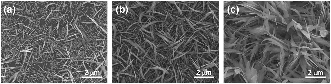 | ||
| Fig. 3 SEM images of Ag NWs synthesized on graphene at 90 °C for 30 min with different AgNO3 concentrations: (a) 30 mM, (b) 60 mM, and (c) 300 mM. | ||
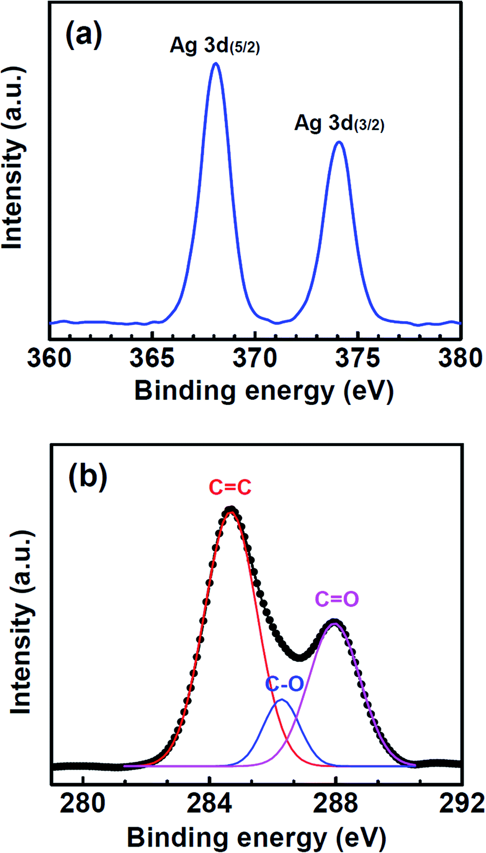
The microstructure of the NWs was investigated by HRTEM, as shown in Fig. 4. The NWs had Ag polycrystalline structure that is less than 100 nm in size. However, Ag2O nanocrystallites were also partially observed. X-ray photoelectron spectroscopy (XPS) study was employed to further understand the chemical states of the NWs and the graphene. With the as-synthesized graphene–Ag NW sample, the Ag 3d5/2 and 3d3/2 peaks were clearly observed at binding energies of 368.1 and 374.1 eV, respectively (Fig. 5(a)). The 368.1 eV of the Ag 3d5/2 peak was in good agreement with the previously reported value (368.0 eV) of Ag0, whereas the corresponding values of AgO and Ag2O were 367.3 and 367.7 eV, respectively.22 This result strongly supports the assertion that the Ag chemical state of NWs consists mainly of metal Ag. The C 1s core level XPS spectrum showed a main peak at 284.5 eV along with a strong shoulder peak on the high binding-energy side (Fig. 5(b)). The deconvolution of the C 1s peak showed three types of carbon bonds: non-functionalized C![[double bond, length as m-dash]](https://www.rsc.org/images/entities/char_e001.gif) C (284.5 eV), hydroxyl carbon C–O (286.2 eV), and carboxylate carbon O–CO (288.0 eV).23,24 We noted that the as-transferred graphene on SiO2/Si substrate showed only a single XPS peak at 284.5 eV (see ESI, Fig. S1(c)†). The typical Raman spectrum of high-quality pristine graphene was also consistent with the XPS result (Fig. S1(a)†). Thus, a significant amount of those functional groups was adsorbed onto the graphene in the reduction reaction solution.
C (284.5 eV), hydroxyl carbon C–O (286.2 eV), and carboxylate carbon O–CO (288.0 eV).23,24 We noted that the as-transferred graphene on SiO2/Si substrate showed only a single XPS peak at 284.5 eV (see ESI, Fig. S1(c)†). The typical Raman spectrum of high-quality pristine graphene was also consistent with the XPS result (Fig. S1(a)†). Thus, a significant amount of those functional groups was adsorbed onto the graphene in the reduction reaction solution.
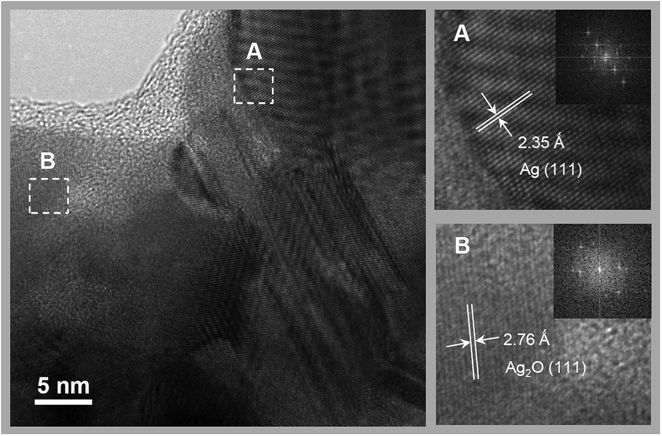 | ||
| Fig. 4 HRTEM images of as-synthesized Ag NWs. The insets show the Fourier transform patterns of lattice images. | ||
 | ||
| Fig. 5 XPS spectra of as-synthesized Ag NWs: (a) Ag 3d and (b) C 1s core levels. | ||
The functional groups on the graphene can act as effective trapping sites for the Ag ions that are attracted by the electrostatic interaction.23 Then, the graphene layer plays a critical role in the growth of Ag NWs by providing excellent path for electrons, as illustrated in Fig. 1(d). The mechanism of the citrate reduction reaction could be expressed as follows: 4Ag+ + Na3C6H5O7 + 2H2O → 4Ag + C6H5O7H3 + 3Na+ + H+ + O2, which can be separated into two reactions made up of an oxidation reaction on the anode (Na3C6H5O7 + 2H2O → C6H5O7H3 + 3Na+ + H+ + O2 + 4e−) and a reduction reaction on the cathode (Ag+ + e− → Ag0). Electrons generated in the oxidation reaction can move freely on the conducting graphene and will quickly reduce the chemi- and physi-absorbed Ag ions. By contrast, the reduction reaction on insulated SiO2 was unfavorable. It is noteworthy that the initially synthesized Ag NWs appeared as very thin sheets and flakes that were strongly attached to the graphene (Fig. 2(a)), while the Ag sediments collected in solution appeared to be only spherical particles (see ESI, Fig. S2†). Those results show how the initial growth of Ag NWs is strongly affected by the Ag ions anchored on graphene. Once precipitated, the Ag clusters and NWs on graphene served as the catalyst for further reduction reactions. Such an autocatalytic reaction can be more enhanced on the sharp tips and along the edges of the Ag NWs due to their high surface energy,18,25 resulting in large-aspect-ratio NWs. In particular, the sharp tips will be the most favorable reduction sites for Ag+ ions because of their highest surface energy nature. However, at a very high Ag+ ion concentration, the autocatalytic reaction rates along the edges will be comparable to those on the tips. As a result, Ag NW seeds developed into Ag sheets and flakes at a high AgNO3 concentration of 300 mM, as shown in Fig. 3(c).
To maximize the conductivity of the graphene–Ag NW hybrid films, the Ag2O nanocrystallites partially existing in NWs and the functional-group-modified graphene film were reduced via thermal annealing under a mixture of H2 and Ar gas flow. HRTEM analysis confirmed that the NWs were completely reduced to pure metal Ag, as shown in Fig. 6. The diffraction patterns were in good agreement with the typical pattern of a face-centered-cubic Ag polycrystals (Fig. 6(a)), which were also consistent with X-ray diffraction (XRD) pattern result (see ESI, Fig. S3†). The crystallinity of NWs was enhanced as well. Fig. 6(b) shows the scanning TEM (STEM) image and the corresponding energy-dispersive spectroscopy (EDS) mapping images of Ag and O elements. The O elements of the NWs were detected as the background limit, indicating below the detection limit of the TEM EDS. The XPS analysis was also consistent with HRTEM results (see ESI, Fig. S4†). The Ag 3d5/2 and 3d3/2 peaks were observed at 368.4 and 374.4 eV, respectively. Moreover, the FWHM (1.2 eV) of the Ag 3d5/2 peak became narrower than that (1.7 eV) of the as-grown NWs, indicating that Ag2O was reduced. After reduction treatment at 300 °C, the functional groups on the graphene were also significantly desorbed (Fig. S4†). The quantitative XPS analysis indicated that the annealed NW sample possessed much lower O concentration (27 at%) than that (49 at%) of the as-grown NW sample. The Ag and C concentrations of the annealed NW sample were 43 at.% and 30 at.%, respectively.
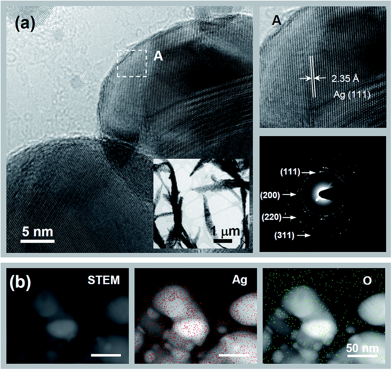 | ||
| Fig. 6 (a) HRTEM images and selective-area diffraction pattern of annealed Ag NWs. The inset shows a low-magnification TEM image. (b) STEM image and the corresponding EDS elemental map for Ag and O composition. | ||
The graphene–Ag NW hybrid film reduced at 300 °C showed an excellent sheet electrical resistance of 54 Ω sq−1, by comparison with pristine graphene film that yielded a sheet resistance of 1.2 kΩ sq−1 (Fig. 7(b)). However, the light transmittance of the graphene–Ag NW hybrid film was as low as 60% at 550 nm (Fig. 7(a)). The pristine graphene film showed an extremely high light transmittance of 97.2% at 550 nm, corresponding to approximately one layer of ideal graphene film. The result was consistent with the Raman spectrum and HRTEM results of the pristine graphene film (Fig. S1†). Such a relatively low light transmittance of the graphene–Ag NW hybrid film is attributed to the highly dense Ag NWs that were synthesized at 60 mM of AgNO3 for 30 min (see ESI, Fig. S5†). Depending on the density of Ag NWs, it is generally accepted that the sheet resistance of graphene–Ag NW films represents a trade off with the low level of light transmittance. Note that our synthesis method allows control of the density and size of Ag NWs via the growth time and AgNO3 concentration, as discussed earlier. Nevertheless, we investigated the effect of graphene–Ag NW patterns as an alternative way to enhance light transmittance with the least sacrifice of sheet resistance. In fact, one of the great merits of our synthesis method involves the easy fabrication of various patterns of graphene–Ag NW electrodes through the simple and self-selective growth of Ag NWs on pre-patterned graphene. For pattern B shown in Fig. 1(b), the light transmittance was dramatically increased to 82% at 550 nm, while the sheet resistance was only slightly increased to 66 Ω sq−1. For pattern A shown in Fig. 1(a), the light transmittance reached 91.5% at 550 nm, despite a low sheet resistance of 102 Ω sq−1. The performance is comparable to that of mechanically-assembled graphene–Ag NW electrodes8,10,14 (see ESI, Fig. S6†). Moreover, it is noteworthy that the ability to directly grow Ag NWs on graphene provides a simple and cost-effective method for the fabrication of graphene-based transparent electrodes.
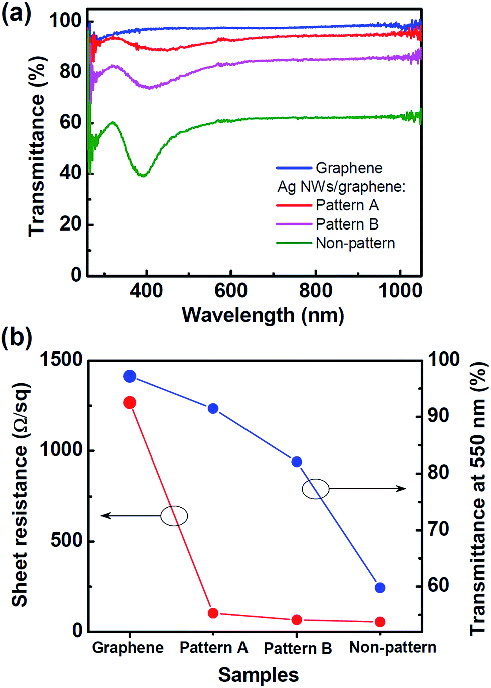 | ||
| Fig. 7 (a) Light transmittance spectra and (b) sheet resistance and light transmittance at 550 nm of pristine graphene, and pattern A, pattern B, and non-patterned samples of graphene–Ag NW films. | ||
Experimental
Preparation of patterned graphene
Graphene was synthesized on Cu foil (Alfa Aesar) by ICP CVD. The graphene on the Cu foil was subsequently transferred to SiO2/Si and glass substrates. Details of the graphene synthesis and transferring process were previously reported.26 The desirable patterns of graphene were formed on the SiO2/Si substrate via UV photolithography and plasma etching: a square grid pattern with a lines width of 20 μm and a pitch of 500 μm (pattern A shown in the inset in Fig. 1(a)) and a rectangular grid pattern with a lines width of 200 μm and a pitch of 500 μm (pattern B shown in the inset in Fig. 1(b)). Graphene was successfully etched by Ar plasma using a RF power of 150 W at room temperature for 15 min.Synthesis of Ag NW on graphene
Ag NWs were synthesized on graphene via a reduction of AgNO3 (99.0%, Sigma Aldrich) and trisodium citrate (Na3C6H5O7, 99.0%, Sigma Aldrich). Desired concentrations of the AgNO3 and 40 mM of Na3C6H5O7 were dissolved in deionized (DI) water. A graphene substrate (1 × 1 cm2) was immersed into the AgNO3 solution (20 ml) at 70 °C and was kept for 10 min. Then, 5 ml of Na3C6H5O7 solution was added drop-wise over a period of 10 min. Subsequently, the mixture was heated to 90 °C to synthesize Ag NWs. Then, colorless AgNO3 solution became lightly opaque yellowish (see ESI, Fig. S7†). The graphene substrate was removed after the desired reaction time, rinsed several times with DI water, and dried under ambient air. In order to deoxidize the Ag oxide components of as-synthesized NWs, the samples were annealed at 300 °C for 30 min under a mixture of Ar and H2 (10%) gas flow.Characterization
The morphology of the NWs was observed using a field-emission SEM (Hitachi S-4800) operated at 10 kV. The crystal structures and microstructures of the NWs were investigated using a high-resolution TEM (Tecnai G2 F30 S-Twin) operated at 300 kV and an XRD (Rigaku diffractometer with Cu Kα radiation) operated at 40 kV and 100 mA. Graphene films were characterized using Raman spectroscopy (UniRam spectrometer with an excitation line at 532 nm and cooled CCD detector). The samples were also characterized using an XPS (Thermo Scientific MultiLab 2000 spectrometer) and an optical transmission spectroscopy (Scinco S-3100). To measure electrical resistivities, two parallel electrodes of Ti (10 nm)/Au (100 nm) were prepared on graphene–Ag NW films through DC sputtering deposition with a shadow mask. Current–voltage properties were measured in the range of −2.5 V and +2.5 V using a semiconductor parameter analyzer (HP4145B).Conclusion
We report the direct and self-selective growth of Ag NWs on the pre-patterned graphene of SiO2/Si and glass substrates via a modified citrate reduction reaction approach. The selective growth of Ag NW on graphene patterns can be attributed to a reduction in the reaction of Ag ions trapped by functional groups on conductive graphene followed by a further autocatalytic reaction, whereas reduction reactions can be restricted on insulated SiO2/Si and glass. Patterned graphene–Ag NW hybrid films showed excellent light transmittance of 91.5% at 550 nm and a low sheet resistance of 102 Ω sq−1. Furthermore, the transparent electrode properties can be further optimized by appropriate patterns and by the size and density of the Ag NWs, which was successfully controlled by reaction time and AgNO3 concentration. Our approach provides simple and cost-effective fabrication of both patterned and non-patterned graphene–Ag NW hybrids, which are promising candidates as transparent conducting films for a variety of device applications, such as displays, solar cells, and LEDs.Acknowledgements
This study was supported by Basic Research Program through the National Research Foundation of Korea (NRF) funded by the Ministry of Education (NRF-2015R1D1A1A01059069).References
- D. S. Hecht, L. Hu and G. Irvin, Adv. Mater., 2011, 23, 1482–1513 CrossRef CAS PubMed.
- X. Huang, X. Qi, F. Boey and H. Zhang, Chem. Soc. Rev., 2012, 41, 666–686 RSC.
- M. F. L. De Volder, S. H. Tawfick, R. H. Baughman and A. J. Hart, Science, 2013, 339, 535–539 CrossRef CAS PubMed.
- L. Dong, Z. Chen, D. Yang and H. Lu, RSC Adv., 2013, 3, 21183–21191 RSC.
- Y. Xu and J. Liu, Small, 2016, 12, 1400–1419 CrossRef CAS PubMed.
- Y. Ahn, Y. Jeong and Y. Lee, ACS Appl. Mater. Interfaces, 2012, 4, 6410–6414 CAS.
- T. Hoon Seo, B. Kyoung Kim, G. Shin, C. Lee, M. Jong Kim, H. Kim and E.-K. Suh, Appl. Phys. Lett., 2013, 103, 051105 CrossRef.
- M.-S. Lee, K. Lee, S.-Y. Kim, H. Lee, J. Park, K.-H. Choi, H.-K. Kim, D.-G. Kim, D.-Y. Lee, S. Nam and J.-U. Park, Nano Lett., 2013, 13, 2814–2821 CrossRef CAS PubMed.
- R. R. Nair, P. Blake, A. N. Grigorenko, K. S. Novoselov, T. J. Booth, T. Stauber, N. M. R. Peres and A. K. Geim, Science, 2008, 320, 1308 CrossRef CAS PubMed.
- I. N. Kholmanov, C. W. Magnuson, A. E. Aliev, H. Li, B. Zhang, J. W. Suk, L. L. Zhang, E. Peng, S. H. Mousavi, A. B. Khanikaev, R. Piner, G. Shvets and R. S. Ruoff, Nano Lett., 2012, 12, 5679–5683 CrossRef CAS PubMed.
- C. Jeong, P. Nair, M. Khan, M. Lundstrom and M. A. Alam, Nano Lett., 2011, 11, 5020–5025 CrossRef CAS PubMed.
- I. K. Moon, J. I. Kim, H. Lee, K. Hur, W. C. Kim and H. Lee, Sci. Rep., 2013, 3, 1112 Search PubMed.
- K. Naito, N. Yoshinaga, E. Tsutsumi and Y. Akasaka, Synth. Met., 2013, 175, 42–46 CrossRef CAS.
- H.-W. Tien, S.-T. Hsiao, W.-H. Liao, Y.-H. Yu, F.-C. Lin, Y.-S. Wang, S.-M. Li and C.-C. M. Ma, Carbon, 2013, 58, 198–207 CrossRef CAS.
- B.-T. Liu and H.-L. Kuo, Carbon, 2013, 63, 390–396 CrossRef CAS.
- J. Liang, L. Li, K. Tong, Z. Ren, W. Hu, X. Niu, Y. Chen and Q. Pei, ACS Nano, 2014, 8, 1590–1600 CrossRef CAS PubMed.
- Y. H. Feng Yi, J. Mater. Sci., 2004, 39, 3241–3243 CrossRef.
- D. Durhuus, M. V. Larsen, A. Andryieuski, R. Malureanu, F. Pizzocchero, P. Bøggild and A. V. Lavrinenko, J. Electrochem. Soc., 2015, 162, D213–D217 CrossRef CAS.
- T. Wu, H. Shen, L. Sun, B. Cheng, B. Liu and J. Shen, ACS Appl. Mater. Interfaces, 2012, 4, 2041–2047 CAS.
- Y.-L. Huang, A. Baji, H.-W. Tien, Y.-K. Yang, S.-Y. Yang, S.-Y. Wu, C.-C. M. Ma, H.-Y. Liu, Y.-W. Mai and N.-H. Wang, Carbon, 2012, 50, 3473–3481 CrossRef CAS.
- H. Wang, X. Qiao, J. Chen, X. Wang and S. Ding, Mater. Chem. Phys., 2005, 94, 449–453 CrossRef CAS.
- G. B. Hoflund, Z. F. Hazos and G. N. Salaita, Phys. Rev. B: Condens. Matter Mater. Phys., 2000, 62, 11126–11133 CrossRef CAS.
- S. A. You, O. S. Kwon and J. Jang, J. Mater. Chem., 2012, 22, 17805–17812 RSC.
- H.-W. Tien, Y.-L. Huang, S.-Y. Yang, J.-Y. Wang and C.-C. M. Ma, Carbon, 2011, 49, 1550–1560 CrossRef CAS.
- Z. Fan, X. Huang, C. Tan and H. Zhang, Chem. Sci., 2015, 6, 95–111 RSC.
- L. V. Nang and E.-T. Kim, J. Electrochem. Soc., 2012, 159, K93–K96 CrossRef CAS.
Footnote |
| † Electronic supplementary information (ESI) available. See DOI: 10.1039/c6ra28389f |
| This journal is © The Royal Society of Chemistry 2017 |