
 Open Access Article
 This Open Access Article is licensed under a Creative Commons Attribution-Non Commercial 3.0 Unported Licence
Photovoltaic enhancement of bismuth halide hybrid perovskite by N-methyl pyrrolidone-assisted morphology conversion†
Ashish Kulkarni,
Trilok Singh *,
Masashi Ikegami and
Tsutomu Miyasaka*
*,
Masashi Ikegami and
Tsutomu Miyasaka*
Graduate School of Engineering, Toin University of Yokohama, 1614 Kuroganecho, Aoba, Yokohama 225-8503, Japan. E-mail: trilok@toin.ac.jp; miyasaka@toin.ac.jp; Web: http://www.cc.toin.ac.jp/sc/miyasaka/
First published on 31st January 2017
Abstract
Low toxicity and highly stable methylammonium bismuth iodide (MBI) ((CH3NH3)3Bi2I9) as a solution-processable photovoltaic absorber produces hexagonal non-uniform morphology leading to poor interfacial contacts with the electron and hole transporting layers. Herein, we tuned the morphology of MBI perovskite by bringing in a small amount of N-methyl-2-pyrrolidone (NMP) as a morphology controller into the MBI–DMF solution. The incorporation of various concentrations of NMP into the precursor solution was found to control the rate of crystallization. An optimal low concentration of 2.5% NMP added to the MBI–DMF precursor solution showed a 50% enhancement in short-circuit current (Jsc). The device showed power conversion efficiencies up to 0.31% with high reproducibility. Moreover, the devices were quite stable when exposed to an ambient atmosphere (relative humidity of 50–60%) for 30 days.
Ever since our pioneering work on perovskite solar cells in a liquid junction that achieved 3.8% power conversion efficiency (PCE)1 the perovskite photovoltaic research has gained enormous attention worldwide2,3 with a certified efficiency climb up to 22.1% in just 7 years.4 Such high efficiency in these devices is attributed to long diffusion length5 and high mobility6 of charge carriers. Simple solution processes adopted for perovskite preparation offer wider choices to control various parameters to engineer the devices.7 However, the toxicity of lead (Pb) and device instability stand as major obstacles for industrialization of this rising material. To improve stability various attempts like replacing methylammonium iodide (MAI) with formamidinium iodide (FAI),8 using insulating Al2O3 instead of UV-sensitive TiO2,9 developing novel hole transporting material (HTM),10 interfacial engineering,11 and developing 2-D based perovskites12 have been made. While some work on stability of Pb based perovskite has shown promising results, replacement of the toxic Pb with other non-toxic metals still remains a big challenge. Although tin (Sn) based perovskite cells have been reported to show PCE up to 10% the problem associated with it is the instability of Sn(II), which gets readily oxidized to Sn(IV) when exposed to air.13,14 Moreover, commercialization of Sn(II) based perovskite can be acutely more toxic than lead(II) because the oxidation of Sn(II) to Sn(IV) can cause reaction with the organism, releasing HI as byproduct, leading to serious damage.15 Recently, copper (Cu) has also been used to replace lead in perovskite structure ((CH3NH3)2CuClxBr4−x). But, its low absorption coefficient and heavy mass of holes limit the device efficiency to low value (0.02%).16
Bismuth (Bi) is the only non-toxic 6p-block element having outer lone pair of 6s2 electron same as lead.17 Recently, researchers have reported promising optoelectronic and photovoltaic properties of methylammonium bismuth iodide (MBI) ((CH3NH3)3Bi2I9) achieving 0.1% efficiency, both in normal and inverted structure, with long term stability.17–19 In previous report, we demonstrated the effect of under layer on the growth of bismuth perovskite and found that growth on anatase TiO2 mesoporous under layer, compared to brookite mesoporous and compact TiO2 (planar architecture) under layer, facilitates better interfacial contacts of MBI with their adjacent connecting layers. As a result, an efficiency of ∼0.2% was achieved with TiO2 anatase porous layer.20 In all reports, MBI films processed by simple solution methods formed hexagonal flakes of MBI, leading to its non-uniform dendritic morphology on porous TiO2.17–20 The key challenges encountered in one-step MBI perovskite spin coating process is to control rapid crystallization of MBI perovskite leading to non homogenous MBI flakes. This is readily evidenced for MBI by the spontaneous formation of an orange perovskite layer, after spin-coating process, whereas in case of lead perovskite complete crystallization of CH3NH3PbI3 is much slower and is achieved on thermal treatment. This difference indicates faster reaction of BiI3, in comparison to PbI2 or PbCl2, with MAI (CH3NH3I−) to form perovskite. As a result, rough surface of MBI perovskite with many pinholes leads to poor device performance. Thus, tuning of morphology is an essential to improve the device performance of MBI perovskite.18–20 Recently, Hoye et al. showed uniform morphology and superior carrier transport property in vapour-processed MBI film although its photovoltaic property was not clarified.21 However, it is of critical importance to develop low cost and rapid solution process in order to obtain smooth and uniform layer of MBI perovskite.
In this article we have investigated the morphological evolution of MBI perovskite via NMP incorporation into MBI and DMF solution and its effect on device performance. NMP which forms complex with lead perovskite, has been used earlier to tune the morphology and obtain highly reproducible device performance in lead based perovskite.22,23 Also, Travis et al. reported the coordination of NMP with bismuth iodide complex24 and from the UV-vis absorption spectra of MBI dissolved in pure NMP, the absorption band at ∼360 nm can be seen (Fig. S1a†) and is different from the absorption spectra of MBI film (Fig. S1b†) which evidently signifies the formation of some complex similar to that of MAPbI3·NMP23 and/or Bi(dppn)I3·NMP.24 Because of high boiling point and low vapour pressure, NMP slowed down the evaporation of solvent mixture during the spin-coating process and facilitated slow crystallization with uniform film formation of MBI perovskite.
In the samples made from solution without NMP additive, we observed no change in colour of the perovskite layer before and after heating at 110 °C for 90 min due to fast crystallization. In contrast, colour of the NMP treated (all concentrations) MBI layer changed from transparent to orange during heating process at the same temperature. The transparent colour of the coated film (before heating) of NMP–DMF MBI might be an intermediate solvated phase formed during perovskite deposition process, similar to lead based perovskite forming complexes with DMSO and NMP.23 This intermediate assisted crystallization is expected to change the morphology of final film which has been evidently observed in scanning electron micrographs (SEM). From Fig. 1a, it is evident that the MBI perovskite without additive has grown into hexagonal flake structure (non-uniform morphology) exposing large area of porous TiO2 through large number of micro-pores, which is in good agreement with the previous reports.17,18,20 In case of NMP guided MBI perovskite (Fig. 1b–d) the change in the morphology has been observed with increasing the concentration of NMP additive. In lower concentration of NMP (1.25% or 12.5 μL mL−1 of precursor solution), MBI perovskite grows into large crystals (Fig. 1b), however this morphology has not observed uniformly over the substrate as shown in Fig. S2.† This indicates that the amount of NMP additive is not sufficiently enough to tune the morphology effectively. Further increasing the concentration of NMP (2.5% or 25 μL mL−1 of precursor solution), the morphology changed drastically (Fig. 1c). In this case the perovskite grain growth is different in comparison to previous 2 cases (non-additive and lower concentration of NMP); the perovskite covered the mesoporous TiO2 layer uniformly. The grain size increased with further increase in the concentration of NMP additive (50 μL mL−1 of precursor solution) as shown in Fig. 1d. The change in the grain growth with NMP concentration is attributed to the change in solubility/interaction of precursor material with the solvent molecule as evident from UV-vis spectra (Fig. S1a†). It has been observed that the colour of precursor solution (MBI–DMF) changes from transparent red to intense red colour with the addition of NMP. Further the rate of evaporation of NMP is slower than the DMF which causes the change in the morphology of MBI films. Although a detail investigation is required and is under progress.
 | ||
| Fig. 1 Top surface SEM images of MBI perovskites without (a) and with different concentration of NMP additives (b–d). | ||
The XRD pattern of MBI films, deposited on mesoporous TiO2 under layer, under different processing conditions are shown in Fig. 2. From the diffraction pattern of non-additive based MBI films we can see a doublet peak at 2θ = ∼12°, which is assigned to MBI perovskite,18,20,25 and its intensity increases with the addition of higher concentration of NMP as shown in zoomed inset figure. In addition to it, intensity of small peak at 2θ = ∼24° also increases with the addition of NMP indicating slight change in the orientation of MBI crystals. From this it is significantly evident that NMP-free MBI films showed poor crystallinity on mesoporous TiO2 layer and with the addition of NMP its crystallinity improved which is suspected due to proper dissolution/interaction of precursor material with addition of NMP, into the main solvent DMF as the colour of the solution changes from red to intense red upon addition of NMP, although detail investigation is required and will be reported separately. The optical absorption spectra showed absorption band around 500 nm for both treated and untreated MBI films, however, a slight increase in absorption is observed for NMP treated (25 μL mL−1) MBI films probably due to the uniform and dense films formation (Fig. S1b†).
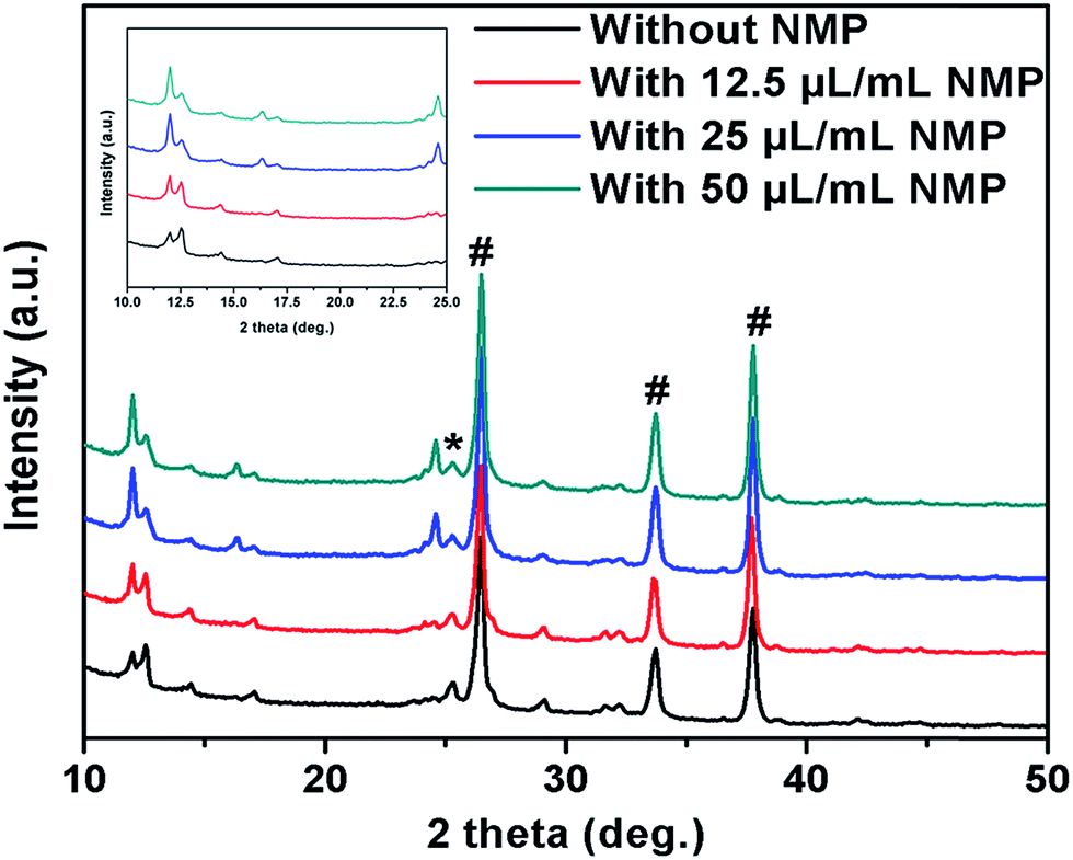 | ||
| Fig. 2 XRD diffraction pattern of MBI layer without and with different concentration of NMP on mesoporous TiO2 coated FTO substrates (# corresponds to FTO peaks and * corresponds to TiO2). | ||
In order to check the influence of tuned morphology and improved crystallization, devices were fabricated by spin coating the MBI solution (with and without additives) on mesostructured substrates and were compared. Detail experimental conditions for device fabrication are given in ESI.† Fig. 3a and b compares the average current density–voltage (J–V) characteristics (Table 1) and external quantum conversion efficiency (EQE) spectra of best performing devices, measured under simulated sunlight intensity of AM1.5 (100 mW cm−2). In all cases studied device showed small hysteresis in J–V characteristic curve which can be due to unbalanced electron and hole flux at the interface of electron- and hole transporting layers26 originating from the energy level mismatch between MBI and its neighboring charge transporting layers.17,20 As can be seen from the histogram plot (Fig. 3c) short circuit photocurrent density (Jsc) of the NMP-free device varied from 0.58 mA cm−2 to 0.68 mA cm−2 with majority of samples showing Jsc of ∼0.62 mA cm−2. With the addition of 1.25% NMP (12.5 μL mL−1) there has been a slight increment in Jsc ranging from 0.6 mA cm−2 to 0.74 mA cm−2. In contrast, addition of 2.5% of NMP drastically improved Jsc to a range from 0.88 mA cm−2 to 1 mA cm−2. Based on the fact of crystallinity and morphology improvement, this increment in Jsc is attributed to better coverage and crystallinity of MBI layer formed on TiO2 scaffold. With further increasing the NMP concentration to 5.0% (50 μL mL−1) the Jsc decreased probably due to the non-smooth region of MBI perovskite layer over the substrate as evidenced in SEM image (Fig. S3†). The EQE spectra of pristine and additive based MBI perovskite have same EQE edge up to ∼650 nm which indicated similar spectral response, however, the EQE increased in visible region for 2.5% NMP-based MBI perovskite. From PCE histogram plot (Fig. 3d), non-additive based MBI perovskite device showed PCE ranging from 0.13% to 0.2% and the PCE of device with 12.5 μL and 50 μL of NMP in 1 mL precursor solution also showed PCE in the same range. Interestingly, device containing MBI perovskite treated with 25 μL of NMP showed PCE ranging from 0.28% to 0.31% with majority of samples showing 0.3% PCE.
 | ||
| Fig. 3 (a) Average J–V curves, (b) IPCE spectra, (c) Jsc and (d) PCE histogram plot of devices containing MBI perovskite without and with different concentration of NMP. | ||
| Case studied | Jsc (mA cm−2) | Voc (V) | FF | PCE (%) |
|---|---|---|---|---|
| Without additive | 0.68 | 0.53 | 0.53 | 0.19 |
| With 12.5 μL NMP | 0.7 | 0.51 | 0.51 | 0.18 |
| With 25 μL NMP | 0.94 | 0.51 | 0.61 | 0.31 |
| With 50 μL NMP | 0.65 | 0.51 | 0.52 | 0.18 |
Long term stability of MBI based devices are investigated by exposing (without encapsulation) to relative 50–60% humidity for 30 days. Device PCE are quite stable (Fig. 4) and NMP treated samples showed improved stability (88% sustained) compared to pristine (66% sustained) which is attributed to high crystallinity of MBI crystals as evidenced from XRD measurement as well as high stable oxidation state of bismuth.17–21
 | ||
| Fig. 4 Long term stability of non-encapsulated MBI devices exposed to 50–60% humidity atmosphere without and with NMP additives. | ||
We could develop a solvent engineering process to prepare uniform MBI absorber for fabrication of non-toxic, highly stable perovskite solar cells. However, device performance is largely behind those of lead perovskite solar cells. Even though MBI perovskite absorbs up to 650 nm it encompasses high carrier density of around ∼1016 cm−3, which are 7 orders of magnitude higher than lead based perovskite.17 Presence of such high density of background charge carriers are mainly responsible for such low Jsc and performance, resulting from bulk recombination within the MBI perovskite, also leading to lower Voc. Hao et al. showed that by tuning and controlling the morphology of tin based perovskite, its background charge carrier density are reduced27 and it is also reported that improving the morphology of MBI can help to reduce the background carrier density18 and our finding reveals that these background charge carriers are slightly reduced to some extent with the addition of NMP indicating that the background charge carrier densities are not highly affected by tuning the morphology unlike tin based perovskite. The exact reason for the slight reduction of background carrier charges, with the addition of NMP, is still unknown but herein we suspect it due to the uniformity and slight change in orientation of MBI film, as revealed by SEM and XRD pattern (Fig. 1 and 2). This further directs the research towards addition of additives and dopants which can reduce the background charge carrier densities similar to the addition of SnF2 in tin based perovskite.14 In addition to the intrinsic property of MBI, the device performance also depends on the charge collecting materials surrounding the MBI in aspects of interfacial contacts and energy level matching.17,20 Non-additive MBI samples, on mesoporous TiO2 layer, showed poor crystallinity as evidenced from XRD plot (Fig. 2). This also suggests choice of suitable electron transporting layer (ETL) and also hole transporting layer (HTL) due to the energy level mismatch between MBI and spiro-OMeTAD, leading to lower Voc.
To summarize, addition of different concentration of NMP into the precursor solution of MBI perovskite, facilitated slow and uniform crystallization resulting in improved morphology and crystallinity of MBI perovskite. The improved morphology of MBI at a particular concentration of 25 μL NMP in 1 mL of precursor solution resulted in enhancement in Jsc and its concomitant enhancement in PCE to 0.31%. Additionally, devices with NMP treated MBI perovskite are highly stable up to 30 days with exposure to relative 50–60% humidity atmosphere. This study opens up the possibilities of tuning the morphology and stability of MBI perovskite. It also directs research towards minimization of the background carrier density and selection of suitable charge collecting materials for further enhancement of efficiency of MBI perovskite solar cells.
Conflict of interest
The authors declare no competing financial interest.Acknowledgements
This study was supported by Japan Science and Technology Agency (JST) Advanced Low Carbon Technology R&D program (ALCA). T. M. thanks the support of Japanese Society for Promotion of Science (JSPS) Grant-in-Aid for Scientific Research B Grant Number 26289265. A. K. thanks Miss Bhumika Chaudhary for her discussion and help in experiments. T. S. thanks to Japanese Society for Promotion of Science (JSPS) for foreign post-doctoral fellowship.References
- A. Kojima, K. Teshima, Y. Shirai and T. Miyasaka, J. Am. Chem. Soc., 2009, 131, 6050 CrossRef CAS PubMed.
- T. Miyasaka, Chem. Lett., 2015, 44, 720 CrossRef CAS.
- T. Singh, J. Singh and T. Miyasaka, ChemSusChem, 2016, 9, 2559 CrossRef CAS PubMed.
- Best solar cell efficiency chart, available at http://www.nrel.gov/ncpv/images/efficiency_chart.jpg, accessed on, 7th Nov. 2016.
- S. D. Stranks, G. E. Eperon, G. Grancini, C. Menelaou, M. J. P Alcocer, T. Leijtens, L. M. Herz, A. Petrozza and H. J. Snaith, Science, 2013, 342, 341 CrossRef CAS PubMed.
- G. C. Xing, N. Mathews, S. Y. Sun, S. S. Lim, Y. M. Lam, M. Grätzel, S. Mhaisalkar and T. C. Sum, Science, 2013, 342, 344 CrossRef CAS PubMed.
- S. Y. Sun, T. Salim, N. Mathews, M. Duchamp, C. Boothroyd, G. C. Xing, T. C. Sum and Y. M. Lam, Energy Environ. Sci., 2014, 7, 399 CAS.
- N. J. Jeon, J. H. Noh, W. S. Yang, Y. C. Kim, S. Ryu, J. Seo and S. I. Seok, Nature, 2015, 517, 476 CrossRef CAS PubMed.
- M. L. Lee, J. Teuscher, T. Miyasaka, T. N. Murakami and H. J. Snaith, Science, 2012, 338, 643 CrossRef CAS PubMed.
- P. Ganesan, K. Fu, P. Gao, I. Raabe, K. Schenk, R. Scopelliti, J. Luo, L. H. Hong, M. Grätzel and M. K. Nazeeruddin, Energy Environ. Sci., 2015, 8, 1986 CAS.
- A. Kulkarni, A. Jena, H.-W. Chen, Y. Sanehira, M. Ikegami and T. Miyasaka, Sol. Energy, 2016, 136, 379 CrossRef CAS.
- D. H Cao, C. C. Stoumpos, O. K. Farha, J. T. Hupp and M. G. Kanatzidis, J. Am. Chem. Soc., 2015, 137(24), 7843 CrossRef PubMed.
- F. Hao, C. C. Stoumpos, D. H. Cao, R. P. H. Chang and M. G. Kanatzidis, Nat. Photonics, 2014, 8, 489 CrossRef CAS.
- M. H. Kumar, S. Dharani, W. L. Leong, P. P. Boix, R. R. Prabhakar, T. Baikie, C. Shi, H. Ding, R. Ramesh, M. Asta, M. Graetzel, S. G. Mhaisalkar and N. Mathews, Adv. Mater., 2014, 26(41), 7122 CrossRef CAS PubMed.
- A. Babayigit, A. Ethirajan, M. Muller and B. T. Conings, Nat. Mater., 2016, 15, 247 CrossRef CAS PubMed.
- D. Cortecchia, H. Dewi, J. Yin, A. Bruno, S. Chen, T. Baikie, P. Boix, M. Graetzel, S. Mhaisalkar, C. Soci and N. Mathews, Inorg. Chem., 2016, 55, 1044 CrossRef CAS PubMed.
- M. Lyu, J.-H. Yun, M. Cai, Y. Jiao, P. V. Bernhardt, M. Zhang, Q. Wang, A. Du, H. Wang, G. Liu and L. Wang, Nano Res., 2016, 9, 692 CrossRef CAS.
- B.-W. Park, B. Philippe, X. Zhang, H. Ransmo, G. Boschloo and E. M. J. Johansson, Adv. Mater., 2015, 27, 6806 CrossRef CAS PubMed.
- S. Öz, J. C. Hebig, F. E. Jung, T. Singh, A. Lepcha, S. Olthof, J. Flohre, Y. Gao, R. German, P. H. M. van Loosdrecht, K. Meerholz, T. Kirchartz and S. Mathur, Solar Energy Materials and Solar Cells, 2016, 158, 195 CrossRef.
- T. Singh, A. Kulkarni, M. Ikegami and T. Miyasaka, ACS Appl. Mater. Interfaces, 2016, 8(23), 14542 CAS.
- R. L. Z. Hoye, R. E. Barndt, A. Osherov, V. Stevanović, S. D. Stranks, M. W. B. Wilson, H. Kim, A. J. Akey, J. D. Perkins, R. C. Kurchin, J. R. Poindexter, E. N. Wang, M. G. Bawendi, V. Bulović and T. Buonassisi, Chem.–Eur. J., 2016, 22, 2605 CrossRef CAS PubMed.
- Y.-J. Jeon, S. Lee, R. Kang, J.-E. Kim, J.-S. Yeo, S.-H. Lee, S.-S. Kim, J.-M. Yun and D.-Y. Kim, Sci. Rep., 2014, 4, 6945 CrossRef PubMed.
- Y. Jo, K. S. Oh, M. Kim, K.-H. Kim, H. Lee, C.-W. Lee and D. S. Kim, Adv. Mater. Interfaces, 2016, 3, 1500768 CrossRef.
- W. Travis, C. E. Knapp, C. N. Savory, A. L. Ganose, P. Kafourou, X. Song, Z. Sharif, J. M. Cockcroft, D. O. Scanlon, H. Bronstein and R. G. Palgrave, Inorg. Chem., 2016, 55, 3393 CrossRef CAS PubMed.
- K. Eckhardt, V. Bon, J. Getzschmann, J. Grothe, F. M. Wisser and S. Kaskel, Chem. Commun., 2016, 52, 3058 RSC.
- J. H. Heo, H. J. Han, D. Kim, T. K. Ahn and S. H. Im, Energy Environ. Sci., 2015, 8, 1602 CAS.
- F. Hao, C. S. Stoumpos, P. Guo, N. Zhou, T. J. Marks, R. H. P. Chang and M. G. Kanatzidis, J. Am. Chem. Soc., 2015, 137, 11445 CrossRef CAS PubMed.
Footnote |
| † Electronic supplementary information (ESI) available: Experimental procedure, top surface SEM images, UV-vis, J–V curve are provided. See DOI: 10.1039/c6ra28190g |
| This journal is © The Royal Society of Chemistry 2017 |