DOI:
10.1039/C6RA28180J
(Paper)
RSC Adv., 2017,
7, 12382-12390
A study on the synthesis, longitudinal optical phonon–plasmon coupling and electronic structure of Al doped ZnS nanorods†
Received
14th December 2016
, Accepted 8th February 2017
First published on 21st February 2017
Abstract
First principles density functional theory (DFT) calculations were employed to study the structural and electronic properties of pure and Al doped ZnS nanorods. The wurtzite-type pure and Al doped ZnS nanorods were synthesized via a hydrothermal method at 175 °C using ethylenediamine as a solvent and complexing ligand. The TEM results reveal that the diameter of the nanorods decreases from 12 to 15 nm with increasing Al doping. It was observed from the UV-Vis spectra of the samples that the energy band gap decreases with Al content. In the Fourier transform infrared (FT-IR) spectra, a noticed splitting of the ZnS peak at 633 cm−1 into three peaks at 489, 613 and 744 cm−1 for the Al doped ZnS nanorods indicates that the Al atom can be partially substituted in the zinc as Al–S–Zn. The atomic concentrations obtained from XPS and EDS are consistent, with XPS demonstrating the successful doping of Al into ZnS. From the XPS, it was observed that the binding energy (BE) values were shifted toward the lower BE side for increasing aluminium content. Raman spectra were obtained for the pure and Al doped ZnS nanorods which exhibit first-order phonon modes at 344.26 and 346.78 for the A1/E1 longitudinal optical phonons, and the bands at 251.14 and 250 cm−1 reveal longitudinal optical phonon–plasmon coupled (LOPC) modes. It was observed that the acceptor level hybridization in Al doped ZnS nanorods occurs due to the overlap of the Al 3s and S 3p states. It was confirmed from XPS and DOS that sulphur vacancies were created due to the doping of Al into the ZnS lattice. It was observed from the band structure of the Al doped ZnS nanorods that the CB and VB bands were almost overlapped in the Brillouin zone at the G-point.
Introduction
In recent years, semiconductor nanostructured materials have attracted great interest attributable to their unique properties which are different from those of bulk materials. At the present time nanoscale semiconductors of group II–VI have received great attention due to their important nonlinear optical properties, luminescence properties, quantum confinement effects, and other important physical and chemical properties. ZnS has two types of structure: hexagonal1 and cubic2 which show wide band gaps of 3.77 eV and 3.72 eV with an exciton binding energy of 40 meV. ZnS has been used for the fabrication of cathode ray tube (CRT) and field emission display (FED) phosphors,3,4 electroluminescent devices, light emitting diodes (LEDs),5 infrared (IR) windows,6 Field Effect Transistors (FETs),7 and sensors.8,9
In the last two decades, much attention has converged on the synthesis of one-dimensional (1D) nanostructured materials, such as nanorods,10,11 nanowires,12,13 nanoribbons,14 and nanotubes.15 These have been synthesized by various techniques such as the chemical co-precipitation method,10 hydrothermal method,16–20 thermal evaporation method,21 pulsed laser deposition,22 electrochemical deposition,23 molecular beam epitaxy (MBE),24 microwave assisted techniques,25 chemical vapor deposition26 etc. This interest is due to their unique properties and applications, which were superior to those of their bulk counterparts. There are various effective methods which have been achieved to develop techniques for the preparation of nanostructures. Recently, metal sulfides have attracted more attention in photocatalysis and antimicrobial activity due to their suitable band gap, catalytic function and toxic nature. Among them ZnS is less toxic and has shown much promise in research activities because of its wide potential applications in nonlinear optical devices, light emitting diodes (LEDs), and solar cells. However, the ZnS nanomaterial is also applicable in photocatalytic reduction because of its electron–hole pair generation capability by photoexcitation without any co-agents. Cubic sphalerite ZnS structures can be obtained under mild conditions and are more stable at room temperature. Hexagonal ZnS structures are obtained at very high temperatures but at low temperature, very few reports are available in the literature.26
In polar semiconductors, the collective oscillations of charge carriers (plasmas) are coupled with longitudinal optical (LO) phonons via the Coulomb interaction. The exploited coupling between longitudinal optical phonons–plasmons in polar semiconductors and the electronic parameters of the material can be extracted via Raman spectroscopy. In polar semiconductors, the long-range electrostatic coulombic force mediates the coupling of LO phonons and the plasmons, which results in the formation of two hybrid excitations of the longitudinal optical phonon–plasmon (LOPC) modes.27 Nevertheless the frequencies of the LOPC modes follow the well-known dispersion relation in an isotropic polar crystal, which has been established for uniaxial crystals like wurtzite ZnO.27
Because of interest in the electronic properties of ordered semiconductors, computational quantum chemical methods such as density functional theory (DFT) have been developed. DFT is one of the most successful approaches to calculate the (ground state) properties of many-electron systems from first principles. DFT was used to collect information from chemistry and physics for the calculation of the electronic structure of atoms and molecules, and it has also been very popular in computational solid-state physics. The exchange–correlation potential describes the effects of the Pauli principle and the Coulomb potential beyond the pure electrostatic interaction of the electrons. A common approximation is the so-called local density approximation (LDA) which locally substitutes the exchange–correlation energy density of an inhomogeneous system by that of an electron gas evaluated at the local density. LDA fails in situations where the density undergoes rapid changes such as in molecules. An improvement to this can be made by considering the gradient of the electron density, the so-called Generalized Gradient Approximation (GGA).28,29
The ZnS band structure can be modulated with certain efforts to meet special characteristics or functions through the doping of different elements: semiconducting materials for the reduction of the band gap and improvements in the electronic structure through the creation of vacancies. These changes help to enhance the response to visible light and the photocatalytic activity.44,57
In this work, we carefully investigate the structural and electronic properties of pure and Al doped ZnS nanorods using experimental techniques as well as first-principles calculations. Also we have investigated the longitudinal optical phonon–plasmon coupled modes from a Raman study of as-synthesized samples. Highly crystalline pure and Al doped ZnS nanorods were synthesized via a hydrothermal method at a temperature of 175 °C. The TEM study candidly demonstrates that the samples exhibit a nanorod morphology.
Experimental details
Preparation of samples
A hydrothermal method was used to synthesize the pure and Al doped ZnS nanorods. In a typical synthesis process a 100 ml Teflon-lined stainless steel autoclave was used. All of the chemicals were of analytical grade and were used without any further purification. The reaction was carried out as appropriate amounts of zinc nitrate (1 − x mmol), aluminium nitrate (x = 0.00, 0.04 mmol) and thiourea (2 mmol) were dissolved in 75 ml deionized (DI) water and ethylenediamine (1![[thin space (1/6-em)]](https://www.rsc.org/images/entities/char_2009.gif) :1 ratio) solution. Then two solutions of the same amount were prepared, these solutions were stirred for 20 min using magnetic stirrer at room temperature and these dispersed solutions were transferred in two autoclaves separately. Then these autoclaves were sealed and kept in a furnace at a temperature of 175 °C for 8 hours, and then allowed to cool naturally. Then the obtained product was centrifuged, washed with ethanol and DI water and then filtered. This final product was dried in a vacuum for 2 hours at 60 °C.
:1 ratio) solution. Then two solutions of the same amount were prepared, these solutions were stirred for 20 min using magnetic stirrer at room temperature and these dispersed solutions were transferred in two autoclaves separately. Then these autoclaves were sealed and kept in a furnace at a temperature of 175 °C for 8 hours, and then allowed to cool naturally. Then the obtained product was centrifuged, washed with ethanol and DI water and then filtered. This final product was dried in a vacuum for 2 hours at 60 °C.
Characterization of samples
As synthesized samples were characterized using different characterization techniques. XRD patterns were recorded using a Bruker AXS D8 Advance powder diffractometer (CuKα1 X-ray tube). Fourier transform infrared (FTIR) transmittance spectra were obtained with a Bruker Vertex 70 spectrometer. UV-Vis absorption spectra were acquired using a Perkin Elmer lambda-950 UV-Vis spectrophotometer. Electron Spectroscopy for Chemical Analysis (ESCA) was performed using an X-ray photon energy of Al Kα: 1486.61 eV, 13 kV, and 300 W from SPECS Surface Nano Analysis GmbH, Germany. Transmission electron microscopy (TEM) measurements were undertaken at an accelerating voltage of 200 kV and selected-area electron diffraction (SAED) patterns were acquired with a Tecnai G2 20 at an acceleration voltage at 200 kV. The energy dispersive spectra (EDS) were collected using a JEOL JSM-6360 SEM.
DFT computational details
The first principle calculations were performed on the basis of density functional theory using the Vienna Ab initio Simulation Package (VASP). The Perdew–Burke–Ernzerhof28,29 (PBE) implementation of the generalized gradient approximation (GGA) was used as the exchange–correlation functional together with the projector-augmented wave (PAW) potential for description of the interactions of the core electrons. The kinetic energy for the cutoff of the plane-wave basis set was set to 500 eV. A 2 × 2 × 2 Γ-centred k-point mesh generated from the Monkhorst–Pack scheme was utilized for all calculations and integrations over the Brillouin zones of the ZnS and Al doped ZnS nanorods, providing a spacing of 0.02 Å−1. The relaxation convergence of energy was taken as 1.0 × 10⁻⁵ eV. The same set of k-points was used in the calculation of the density of states (DOS). The DOS of each system was modelled from the fully geometry optimized state. The hexagonal structure for the pure and Al doped ZnS nanorods was constructed on the basis of supercells containing 32 atoms. Using an experimental finding we have modelled the wurtzite-type morphology for pure and Al doped ZnS nanorods along the [0001] direction. A Methfessel–Paxton smearing method and normal algorithm (blocked Davidson) was used for all calculations with a smearing width of 0.15 eV.
Results and discussion
X-ray diffraction study
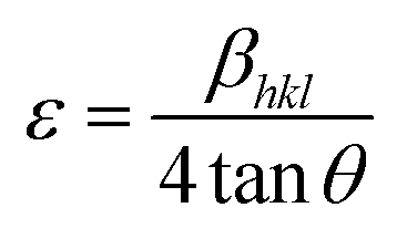
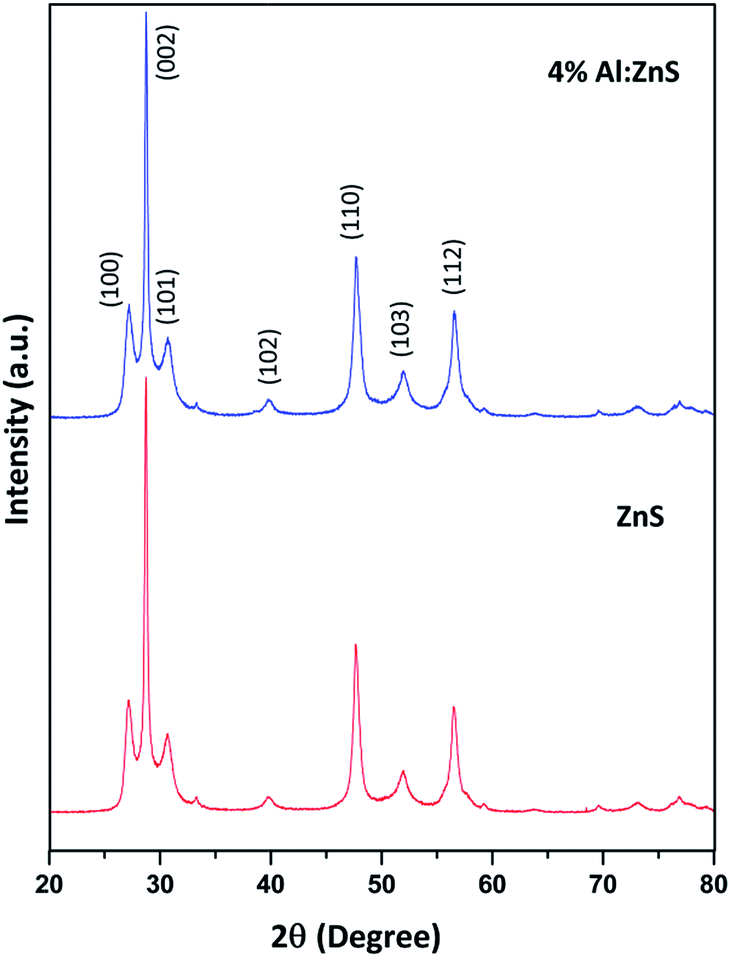
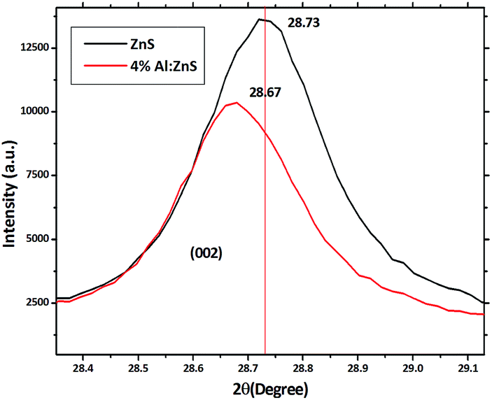
The XRD patterns of the pure and Al doped ZnS nanorods can be seen in Fig. 1. All the diffraction peaks can be readily indexed to the hexagonal wurtzite phase structure, which are consistent with the standard card (JCPDS no. 36-1450). The X-ray diffraction patterns were recorded by using CuKα1 radiation with λ = 1.5406 Å. No secondary phases were observed in the as-synthesized samples. It is possible to predict the growth direction from the comparison of the full width at half maximum (FWHM) of different XRD peaks. Here the (002) diffraction peak intensity is very high and narrower in width than the other peaks which suggests a preferential growth direction along the c-axis, which is further demonstrated below by our TEM study. Also the typical (002) diffraction peak shifted towards the lower angle, as shown in Fig. 2. This shift towards a lower angle was believed to result from the incorporation of Al ions into the ZnS lattice and due to variation in the lattice constant which can be attributed to the non-uniform substitution of Al3+ ions into the zinc ion site as the radius of the Al3+ ion (67.5 pm) is smaller than that of the Zn2+ ion (75 pm). The lattice constants ‘a’ increased and ‘c’ decreased with Al content. A variation in the lattice parameters indicates that a number of Al atoms have been successfully incorporated into the Al doped ZnS host, which is consistent with the relations of Vegard’s law, as summarized in Table 1. Furthermore, an abnormal increase of the lattice constant ‘a’ of the Al doped ZnS sample can be regarded as the surface tension induced by its typical morphology. As explained earlier, due to the smaller size of the Al3+ ions compared to that of the Zn2+ ions, incorporation of Al atoms into ZnS leads to a slight change in the lattice constants of ZnS, resulting in an enhancement in the micro-strain for the Al doped ZnS nanorods. Lattice parameters obtained from XRD data and chemical compositions from XPS and EDS are summarized in the Table 1. The c/a ratio suggests a hexagonal closed packed structure. It is known that when the bonding character is more ionic then the c/a ratio moves towards the ideal values. In our case c/a ratio values are well matched to the ideal value of 1.6333. The u-parameter arises from the c-axis cation displacement which is caused by deviation of the anion position from its ideal value of 0.375, in our case it is found that the values are in agreement with ideal values.30a Further the strains in the nanorods were calculated from the XRD data using the Stokes–Wilson relation (1), which shows that the micro-strain was increased with Al content.30a| |
 | (1) |
where ε is strain in the samples and βhkl is the full width at half maximum at angle 2θ on the XRD patterns of samples.
 |
| | Fig. 1 XRD patterns of the pure and Al doped ZnS nanorods evincing their hexagonal structures. | |
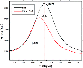 |
| | Fig. 2 Magnified plot of Fig. 1 showing a shift in the (002) peak position towards the lower angle side. | |
Table 1 The lattice parameters from the XRD data, nanorod diameter from the TEM data, and atomic% (at%) of elements from the XPS and EDS data for the pure and Al doped ZnS nanorods
| Samples (x) |
Lattice constants |
Volume of unit cell (Å) |
X-ray density (g m−3) |
c/a ratio |
u-Parameter |
Strain |
TEM diameter (nm) |
XPS (at%) |
EDS (at%) |
| a (Å) |
c (Å) |
Zn |
Al |
S |
Zn |
Al |
S |
| 0.00 |
3.7869 |
6.2088 |
77.109 |
4.1984 |
1.639 |
0.3735 |
0.00162 |
12 |
50.7 |
0.00 |
49.2 |
50.34 |
0.00 |
49.66 |
| 0.04 |
3.7904 |
6.2025 |
77.206 |
4.10379 |
1.637 |
0.3740 |
0.00169 |
15 |
49.58 |
2.01 |
46.07 |
51.41 |
2.22 |
46.37 |
UV-visible absorption spectroscopy
The UV-Vis absorbance spectra of the pure and doped ZnS nanorods were recorded using wavelengths from 200 to 800 nm as shown in Fig. 3. The absorbance peaks were observed at 368 and 371 nm for the pure and Al doped ZnS nanorods respectively. A red shift was observed at the absorption edge to the smaller wavelength side, due to the exchange interaction between the d electrons of the aluminum ions and the s and p electrons of the host electron band. It is well known that ZnS has a direct band gap therefore, the value of n is 1/2 as the transition from the valence band to conduction band is direct. The energy band gap was calculated using the Tauc equation30b (2).where α is the absorption coefficient, hν is the photon energy, A is a band edge sharpness constant and Eg is the energy band gap of the sample. It is found to be 3.51 and 3.43 eV for pure and Al doped ZnS nanorods. The pure and Al doped ZnS samples show red shifts comparable to bulk ZnS (3.77).1 Here, the band gap decreases as the aluminum doping content increases.
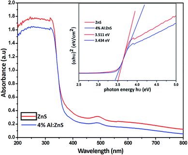 |
| | Fig. 3 UV-Vis absorbance spectra of pure and Al doped ZnS nanorods, inset shows the corresponding Tauc plot for the evaluation of the energy band gap. | |
FT-IR study
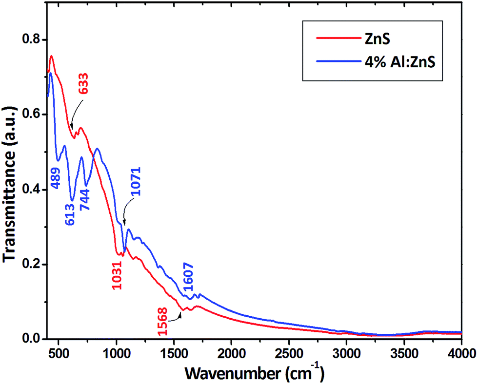
The FT-IR spectra for the as-synthesized samples are shown in Fig. 4. The sharp and strong peaks show that the samples were highly crystalline in nature. The crystallinity was increased with the doping of Al. The characteristic ZnS vibration peaks can be seen at 400–650 cm−1 as shown in Fig. 4.30b–32 The strong and narrow peak at 489 cm−1 corresponds to a weak S–S stretching vibration observed for the Al doped ZnS nanorods. A broad peak at 3350 cm−1 was not found for either sample; this peak is assigned to O–H stretching which can result from small quantities of absorbed water (H2O) in the samples, meaning that the samples here are moisture free. The peaks in the FT-IR spectra of the pure and Al doped ZnS nanorods at 633 and 613 cm−1 can be assigned to the δ(C![[double bond, length as m-dash]](https://www.rsc.org/images/entities/char_e001.gif) S) functional group of thiourea, whereas the peaks at 1050 to 1143 cm−1 are attributed to the stretching mode of ν(CS) for thiourea and the formation of microstructures in the samples.33,34 The bands at 1565 to 1646 cm−1 are due to the –CO stretching mode arising from the adsorption of atmospheric CO2 on the surface of the samples.35–37 The presence of sulfur vacancies in our Al doped ZnS samples confirmed by the results of our FT-IR studies also implies the high emission intensity of electron transfer from the sulfur vacancies to the zinc vacancies. It is noticed that the FT-IR spectrum of the 4% Al doped ZnS nanorods shows similar peaks with respect to that of the pure ZnS nanorods and in addition to that some noticeable new peaks at 489, 613 and 744 cm−1 may be due to the emergence of a resonance interaction due to the differences in the vibrational modes of the zinc and aluminium sulfide ions. This indicates that the Al3+ ions can be partially substituted between the zinc ions as Al–S–Zn, which may be responsible for the splitting of the original ZnS peak at 633 cm−1 into three new peaks, i.e., 489, 613 and 744 cm−1. It was confirmed from the band structure (Fig. 8(a and c))that the distance between the valence band and conduction bands was altered due to the partial substitution of Al ions by Zn ions. The band values are in good agreement with the reported literature.31–37
S) functional group of thiourea, whereas the peaks at 1050 to 1143 cm−1 are attributed to the stretching mode of ν(CS) for thiourea and the formation of microstructures in the samples.33,34 The bands at 1565 to 1646 cm−1 are due to the –CO stretching mode arising from the adsorption of atmospheric CO2 on the surface of the samples.35–37 The presence of sulfur vacancies in our Al doped ZnS samples confirmed by the results of our FT-IR studies also implies the high emission intensity of electron transfer from the sulfur vacancies to the zinc vacancies. It is noticed that the FT-IR spectrum of the 4% Al doped ZnS nanorods shows similar peaks with respect to that of the pure ZnS nanorods and in addition to that some noticeable new peaks at 489, 613 and 744 cm−1 may be due to the emergence of a resonance interaction due to the differences in the vibrational modes of the zinc and aluminium sulfide ions. This indicates that the Al3+ ions can be partially substituted between the zinc ions as Al–S–Zn, which may be responsible for the splitting of the original ZnS peak at 633 cm−1 into three new peaks, i.e., 489, 613 and 744 cm−1. It was confirmed from the band structure (Fig. 8(a and c))that the distance between the valence band and conduction bands was altered due to the partial substitution of Al ions by Zn ions. The band values are in good agreement with the reported literature.31–37
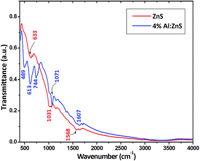 |
| | Fig. 4 Transmittance FTIR spectra of the pure and Al doped ZnS nanorods. | |
XPS study
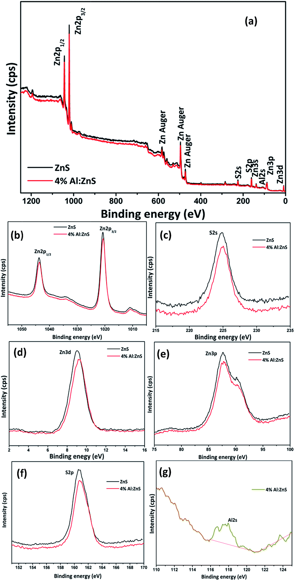
The chemical states of the Zn2+, S2− and Al3+ in the samples were investigated using XPS. The XPS analysis of samples was performed in the range of 0–1250 eV and the survey spectrum is shown Fig. 5(a). It confirms that Zn, S and Al were present in the synthesized samples. No contaminant species were detected within the sensitivity range of the technique. The binding-energy data have been standardized to an energy scale that assumes adventitious carbon C 1s at 284.6 eV. The BE for pure ZnS was observed for Zn 2p1/2 and Zn 2p3/2 at 1043.76 and 1020.73 eV respectively, while for Al doped ZnS the binding energy values were obtained for Zn 2p1/2 and Zn 2p3/2 at 1043.67 and 1020.62 eV respectively. Due to the doping effect the binding energy values shifted gradually to a lower energy. This is also attributed to the presence of some S vacancies.44 From the spectra of Zn 2p in Fig. 5(b), spin–orbit splitting of Zn 2p3/2 and Zn 2p1/2 was found at 23.03, 23.05 eV for pure and Al doped ZnS which suggests the existence of Zn2+.38,39 From Fig. 5(c), for the S 2p peak it was observed that there was overlapping of the spin–orbit doublets. The binding energies of S 2p for the as-synthesized samples are centered at 160.71 and 160.82 eV which are characteristic values of metal sulfide (S2−) species.40–42 The appearance of all the binding energy values for Zn 2p and S 2p are in accordance with previously reported studies.40–42 In Fig. 5(g) the binding energy appears for Al 2s at 177.65 eV corresponding to the +3 oxidation state of Al. The BE values of the pure and 4% Al doped ZnS nanorods for the Zn 3d spectra were found to be 9.027 and 9.3015 eV and for the S 2s spectra were detected as 160.71 and 160.82 eV respectively. Also, the spectra of Zn 3p was found to contain BE values for Zn 3p3/2 at 87.65 and 87.78 and Zn 3p1/2 at 90.28 and 90.32 eV for pure and Al doped ZnS nanorods.43 The detailed elemental compositions were extracted from the XPS and it was found that the at% for S was 49.2 and 46.07; at% for Zn was 50.7 and 49.58 and at% for Al was 0.00 and 2.01 for the pure and Al doped ZnS nanorods respectively.
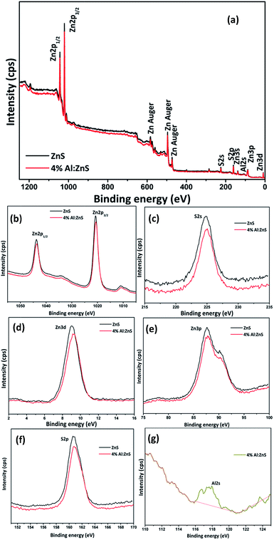 |
| | Fig. 5 (a) Survey, (b) Zn 2p, (c) S 2s, (d) Zn 3d, (e) Zn 3p, (f) S 2p and (g) Al 2s spectra of the pure and Al doped ZnS nanorods. | |
Morphological investigation
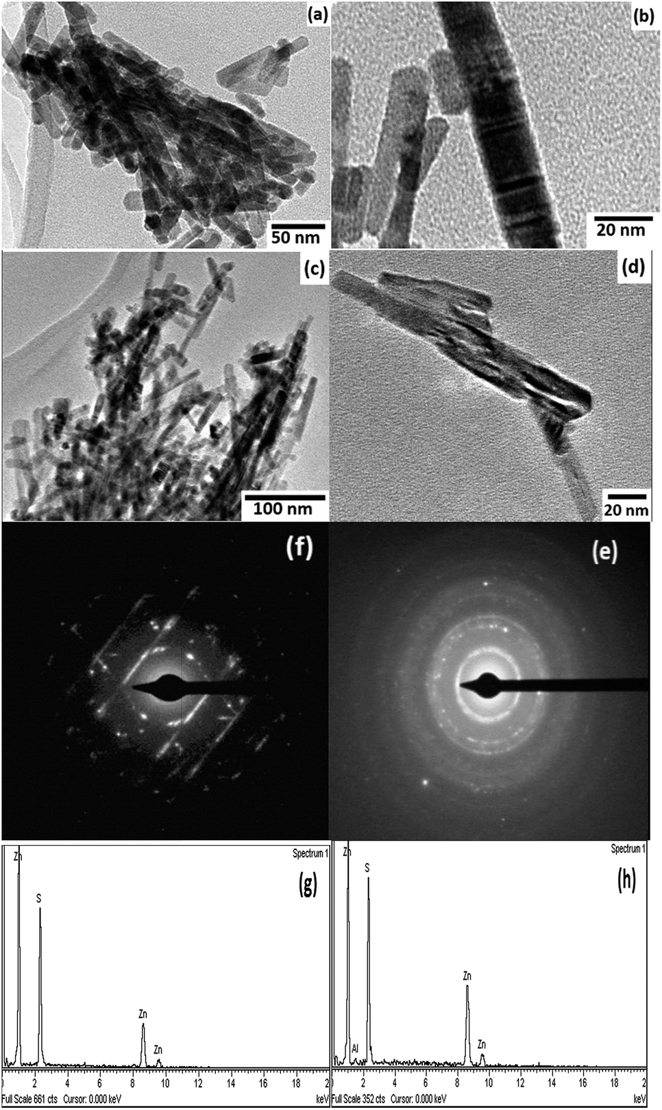
Transmission electron microscopy (TEM) was employed to investigate the structural morphology of the pure and Al doped ZnS samples. TEM images of the samples are shown in Fig. 6(a–d). The TEM micrographs show that the nanorods have uniform diameters. The average diameters for the pure and Al doped ZnS nanorods were found to be 12 nm and 15 nm, respectively, with lengths in the range of tens of nanometers. It was explicitly observed that the diameters of the nanorods were increased with increasing Al content. The selected area electron diffraction (SAED) patterns are depicted in Fig. 6(e and f). The SAED patterns in Fig. 6(e and f) of the samples show concentric rings which demonstrates the polycrystalline nature of the hexagonal structure. Furthermore, the chemical compositions of the pure and Al doped ZnS nanorods were observed from EDS spectra as follows: at% of Zn = 50.34 and 51.41, at% of S = 49.66 and 46.37 and at% of Al = 0.00 and 2.22 for the pure and Al doped ZnS nanorods respectively.
 |
| | Fig. 6 The different magnified TEM images (a) and (b) for pure and (c) and (d) for Al doped ZnS nanorods, (e), (f) and (g), (h) are SAED and EDS patterns of the corresponding pure and Al doped ZnS nanorods, respectively. | |
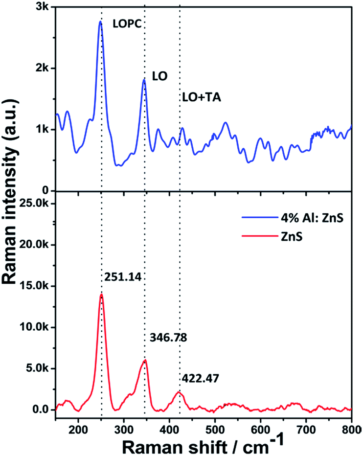
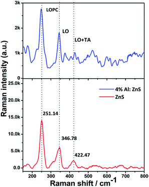
Raman study
Raman shift measurements of the as-synthesized samples were carried out using a red helium–neon (He–Ne) laser with an excitation laser wavelength of 633 nm to study the effects of aluminium substitution in the ZnS nanorods. The room-temperature Raman spectra for the as-synthesized nanorods are shown in Fig. 7. It is known that the wurtzite structure of ZnS belongs to the symmetric space group C46ν (P63mc) in the primitive cell. The zone-centre optical phonon can be classified as the following irreducible representation,| | |
Γopt = A1 + E1 + 2E2 + 2B1
| (3) |
where the A1 and E1 modes are polar modes and are both Raman and infrared active, the E2 modes are nonpolar and Raman active and the B1 modes are silent modes. The A1 and E1 symmetry splits into two components viz. transverse optical (TO) and longitudinal optical (LO), and both of them are highly isotropic, A1(TO) = E1(TO) and A1(LO) = E1(LO), which is a characteristic feature of the wurtzite ZnS. The previously reported values were compared with our experimental values and are given in Table 2.
 |
| | Fig. 7 Room-temperature Raman spectra of pure and 4% Al doped ZnS nanorods, which evince the first-order LO phonon modes. The genuine feature spectral line observed at ∼251 cm−1 for LOPC mode. | |
Table 2 Assignment of Raman modes of ZnS nanorods in air at room temperature. Frequency given in cm−1
| Assignment |
In this work |
Reported |
| Pure ZnS |
Al doped ZnS |
| LA |
Not observed |
Not observed |
110 (ref. 50) |
| 2TA |
Not observed |
Not observed |
139,54 176 (ref. 54) |
| LA |
Not observed |
Not observed |
216,51 217,47,48 219 (ref. 47) |
| LOPC |
251.14 |
250 |
258 (ref. 49) |
| A1/E1(TO) |
Not observed |
Not observed |
269,51 272,44 273,48 276 (ref. 47) |
| E2(TO) |
Not observed |
Not observed |
282,51 284 (ref. 44) |
| A1/E1(LO) |
344.26 |
346.78 |
346.4,51 349.6 (ref. 44) |
| 350,44,47 351,48 352 (ref. 45) |
| SO |
Not observed |
Not observed |
332.9,44 335 (ref. 51) |
| LO + TA |
422.47 |
421 |
418,44 422 (ref. 51) |
| TO + TA |
|
|
386.6 (ref. 44) |
| 2TO |
Not observed |
Not observed |
615,51 617 (ref. 47) |
| TO + LA |
Not observed |
Not observed |
633,51 642 (ref. 47) |
| 2LO |
Not observed |
Not observed |
668,51 673 (ref. 47) |
The longitudinal optical (LO) peaks have been reported to centre at around 350 cm−1 for both the hexagonal and cubic structures of ZnS, and correspond to zone-center (Γ point of the Brillouin zone) phonons.45 Herein, the LO peak was observed at 344.26 cm−1 for the pure ZnS nanorods and 346.78 cm−1 for the 4% Al doped ZnS nanorods. This corroborates that the as synthesized nanorods exhibit a peak shift towards low energy as compared to the Raman spectrum of bulk hexagonal ZnS of LO at 352 cm−1.45,46 The peaks at 251.14 and 250 are due to the polar nature of the wurtzite nanorods. Kumar et al.50 reported coupling between the longitudinal phonons and the charge density modes, namely the L+ and L− modes. As the charge carrier concentration in the semiconductor increases, the frequency of the L+ mode increases from the bulk LO mode frequency and the frequency of the L− mode increases from zero to the mode frequency.50 Hence the peaks at 251.14 and 250 cm−1 observed in the present samples can be tentatively attributed to the LO phonon–plasmon coupled (LOPC) L− mode.50,53 It may be due to the formation of a small portion of the intermediate state due to the incomplete conversion during the synthesis process.54,55 It can be seen from Fig. 7 that the LO mode is more altered while the peak position of the LOPC mode has shifted to lower frequencies with increasing aluminium content. Another reason for the red-shift is that the introduction of host lattice defects such as sulfur and zinc vacancies is due to doping of Al ions into the ZnS lattice. From the DFT calculations, the total density of states shows that sulfur vacancies were created, as the metal ions were doped into the ZnS lattice. In addition, second-order Raman scattering was seen in the range of 350–450 cm−1. This second-order scattering consists of a longitudinal optical + transverse acoustic (LO + TA) phonon mode at ∼422.47 and 421 cm−1 for the pure and Al doped ZnS nanorods. It is similar to the 2LA phonon response. Multi-phonon responses in the range of 350–450 cm−1 are hardly seen because of the strong plasmon background fluctuations in polar semiconducting systems, resulting in two different LOPC modes. It was also observed that the Raman intensity decreases with Al doping in ZnS sites.45–52
Density functional theory
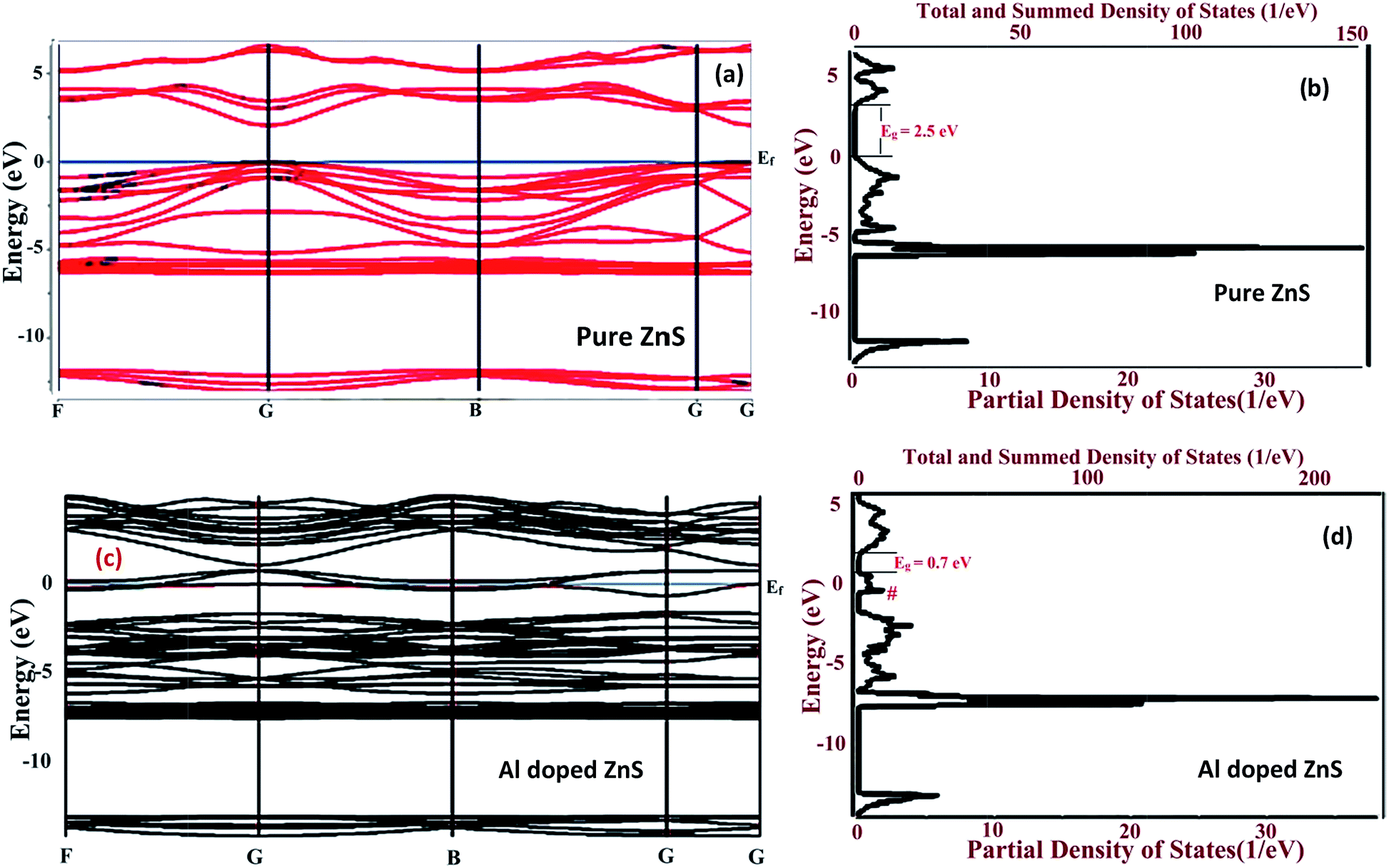
To assure the accuracy of our computational method, we have performed a series of calculations for cell optimization. The structural optimization was first performed for the wurtzite structure of the pure and Al doped ZnS nanorods with the lattice parameters a = 3.8497 and c = 6.3139 Å after optimization, which are in good agreement with XRD results for pure ZnS as a = 3.7869 and c = 6.2088 Å and for Al doped ZnS as a = 3.7904, c = 6.2025 Å. Fig. 8(a and c) illustrates the band structure of the pure and Al doped ZnS nanorods within the GGA-PBE approximation. The Brillouin zone integrations are carried out along the F, G, B, G, G high symmetry path for the pure and Al doped ZnS as shown in Fig. 8(a and c). Supercells of pure and Al doped ZnS nanorods are given in the ESI Fig. S1.† The electronic properties of the wurtzite pure and Al doped ZnS nanorods were investigated and the ZnS nanorods were found to be direct band gap semiconductors. The energy band gap was estimated to be 2.35 eV at the high symmetry G-point in the Brillouin zone for pure ZnS. Lashgari et al.59 reported that for 3D wurtzite-ZnS, the bandgap is 2.14 eV and 2D wurtzite-ZnS has a band gap of 2.77 eV at the PBE-GGA level of theory, also Meng et al.60 reported that bulk W-ZnS has a band gap of 2.09 eV, and our obtained optical gaps are comparable with these results. At the zero position in the band structures of the compounds in Fig. 8(a) and (c) is the Fermi energy level (Ef). From Fig. 8(c) for Al doped ZnS, the calculated band gap values decreased compared to those in Fig. 8(a) (pure ZnS) due to the some levels passing through the Ef. This indicates that Al doped in ZnS acts as an acceptor impurity. Comparing the energy band gap from the TDOS of 2.5 eV for the pure and 0.7 eV for Al doped ZnS nanorods are shown in Fig. 8(b and d). It reveals that the band gap decreases after reporting Al, also at the side of the top of the valence band there are redundant carrier cavity pairs that induced an acceptor band near the Ef.57 Our results from the band structure of ZnS nanorods are in accordance with the results obtained theoretically by Yeh et al.,56 but experimental UV-Vis band gap values were found to be greater than both of the theoretical values in both cases. There are very few reports on Al doped ZnS samples found elsewhere, therefore we obtained very interesting and novel results using DFT calculations. It is well known that the effect of the surface on the physical properties is very important on the nanoscale. The band gap predication from DFT calculations always exists as the result of the well-known limitation for the determination of accurate energy band properties of materials.51 To study the effect of Al on the ZnS lattice, first-principles calculations on the electronic properties of the wurtzite nanorods were performed. The DOS plots for Al doped ZnS, shown in Fig. 8(d), reveal the presence or creation of an S vacancy in 32 atoms per 2 × 2 × 2 supercell of the hexagonal structure. The presence of S vacancy states, which cause visible light absorption,44 may also be helpful in increasing the photocatalytic activity. The narrow band gap and the acceptor states in the band gap are very beneficial for improving the visible-light absorption and photocatalysis.57
 |
| | Fig. 8 (a) and (c) Plots of the band structure, and (b) and (d) plots of total density of states of pure and Al doped ZnS nanorods of the hexagonal structure, (b) for hexagonal Zns, 32 atoms per 2 × 2 × 2 supercell without S vacancies, (d) for Al doped ZnS, 32 atoms per 2 × 2 × 2 supercell with one S vacancy (# indicates the S vacancy). | |
The total density of states (TDOS) of the pure and Al doped ZnS nanorods is shown in Fig. 8(a and c). Doping with Al introduces additional states from the Al 3s and 3p states. It was also observed from the band structure of the Al doped ZnS nanorods that the conduction band (CB) and the valence band (VB) are almost overlapped in the Brillouin zone at the G-point. The Al-related states are well hybridized with the CB and do not extend below the CBM. It was explicitly corroborated that the 3s state contributes more to the TDOS at the CB as compared to 3p states and the same trend was followed for Zn.58
Conclusions
Pure and Al doped ZnS nanorods were synthesized through a hydrothermal method at low temperature (175 °C). The samples have hexagonal closed packed structures. The energy band gap of the pure and Al doped ZnS nanorods shows more red shift as compared to the bulk ZnS band gap. The atomic compositions obtained from XPS and EDS are consistent. XPS revealed the successful doping of Al3+ into the ZnS lattice. The energy band gap was decreased with Al content. From the XPS, it was observed that the binding energy (BE) values were shifted towards the lower BE side for increasing aluminium content and this supports the formation of sulphur vacancies. It was confirmed that chemical species of pure and Al doped ZnS nanorods were detected from FTIR spectra. It has been observed from TEM image analysis that the morphology of the samples are nanorod-like structures. SAED patterns evidence that the as-synthesized samples persist in a hexagonal structure, as evidenced further by TEM and XRD. The Raman spectra obtained from pure and Al doped ZnS nanorods exhibit first-order phonon modes at 344.26 and 346.78 cm−1 corresponding to A1/E1 longitudinal optical phonons and the modes at 251.14 and 250 cm−1 reveal the presence of LO phonon–plasmon coupled (LOPC) modes. It was also confirmed by the LOPC mode that wurtzite ZnS has a polar nature. From DFT calculations, we know that the Al acts as an acceptor impurity, with a narrow band gap, which are very beneficial for improving the visible-light absorption and photocatalytic properties. From DFT, the calculated band gap of the Al doped ZnS nanorods is much smaller than that of the pure ZnS nanorods. It was observed from the band structure of the Al doped ZnS nanorods that the CB and VB approximately overlap at the G-point in the Brillouin zone. It was observed that the acceptor level hybridization in the Al doped ZnS nanorods occurs due to the overlapping of the Al 3s and S 3p states. In the analysis of the electronic structures, an acceptor band is induced because of doping of Al into the ZnS nanorods. The Al acts as an acceptor impurity, has a narrow band gap, and facilitates the creation of sulphur vacancies in the nanorods.
Acknowledgements
The authors are appreciative to UGC-DAE CSR, Indore for financial assistance through Project No. UGC-DAE, CSR-I/CSR-66/2012-13/270. They are also thankful to Dr T. Shripathi and Dr N. P. Lalla, UGC-DAE CSR, Indore for providing XPS and TEM facilities and Prof. S. S. Shah for his assistance.
References
- H. Ong and R. Chang, Appl. Phys. Lett., 2001, 79, 3612 CrossRef CAS.
- T. Tran, W. Park, W. Tong, M. Kyi, B. Wagner and C. Summers, J. Appl. Phys., 1997, 81, 2803 CrossRef CAS.
- Z. Zhong, Science, 2003, 302, 1377–1379 CrossRef CAS PubMed.
- Y. Cui, Z. Zhong, D. Wang, W. Wang and C. Lieber, Nano Lett., 2003, 3, 149–152 CrossRef CAS.
- P. Calandra, M. Goffredi and V. Liveri, Colloids Surf., A, 1999, 160, 9–13 CrossRef CAS.
- Y. Cui, Science, 2001, 293, 1289–1292 CrossRef CAS PubMed.
- Z. Chen, L. Cheng, H. Xu, J. Liu, J. Zou, T. Sekiguchi, G. Lu and H. Cheng, Adv. Mater., 2010, 22, 2376–2380 CrossRef CAS PubMed.
- Q. Wang, B. Liu, X. Wang, S. Ran, L. Wang, D. Chen and G. Shen, J. Mater. Chem., 2012, 22, 21647 RSC.
- M. Ruedas-Rama, A. Orte, E. Hall, J. Alvarez-Pez and E. Talavera-Rodriguez, Biophys. J., 2011, 100, 468a–469a CrossRef.
- S. Acharya, N. Maheshwari, L. Tatikondewar, A. Kshirsagar and S. Kulkarni, Cryst. Growth Des., 2013, 13, 1369–1376 CAS.
- M. Limaye, S. Gokhale, S. Acharya and S. Kulkarni, Nanotechnology, 2008, 19, 415602 CrossRef PubMed.
- D. Wu, Y. Jiang, Y. Zhang, Y. Yu, Z. Zhu, X. Lan, F. Li, C. Wu, L. Wang and L. Luo, J. Mater. Chem., 2012, 22, 23272 RSC.
- J. Kim, S. Kim, D. Kim, K. Oh, W. Hong, T. Bae and H. Chung, J. Nanomater., 2016, 2016, 1–6 Search PubMed.
- U. Gawai, H. Khawal, T. Shripathi and B. Dole, CrystEngComm, 2016, 18, 1439–1445 RSC.
- S. Kar and S. Chaudhuri, J. Phys. Chem. B, 2005, 109, 3298–3302 CrossRef CAS PubMed.
- S. Acharya, S. Bhoga and K. Singh, Integr. Ferroelectr., 2010, 116, 16–22 CrossRef CAS.
- S. Pahari, A. Sinhamahapatra, N. Sutradhar, H. Bajaj and A. Panda, Chem. Commun., 2012, 48, 850–852 RSC.
- W. Xuan-Rong, Y. Qiao-Zhen, Z. Yong-Xiang and L. Yan-Luo, J. Inorg. Mater., 2016, 31, 473 CrossRef.
- M. Wei, J. Yang, Y. Yan, J. Cao, Q. Zuo, H. Fu, B. Wang and L. Fan, Superlattices Microstruct., 2013, 54, 181–187 CrossRef CAS.
- J. Cao, L. Fan, J. Yang, Y. Yan, M. Wei, L. Yang, B. Feng, D. Han, B. Wang and H. Fu, Superlattices Microstruct., 2013, 57, 58–65 CrossRef CAS.
- M. Lu, L. Chen, W. Mai and Z. Wang, Appl. Phys. Lett., 2008, 93, 242503 CrossRef.
- X. Xu, G. Fei, W. Yu, X. Wang, L. Chen and L. Zhang, Nanotechnology, 2005, 17, 426–429 CrossRef.
- R. Chen, D. Li, B. Liu, Z. Peng, G. Gurzadyan, Q. Xiong and H. Sun, Nano Lett., 2010, 10, 4956–4961 CrossRef CAS PubMed.
- C. Bradford, C. O’Donnell, B. Urbaszek, A. Balocchi, C. Morhain, K. Prior and B. Cavenett, J. Cryst. Growth, 2001, 228, 634–638 CrossRef.
- P. Calandra, M. Goffredi and V. L. Turco, Colloids Surf., A, 1999, 160, 9–13 CrossRef CAS.
- U. Gawai, H. Khawal, M. Bodke, K. Pandey, U. Deshpande, N. Lalla and B. Dole, RSC Adv., 2016, 6, 50479–50486 RSC.
- A.-J. Cheng, Y. Tzeng, H. Xu, S. Alur, Y. Wang, M. Park, T. Wu, C. Shannon, D.-J. Kim and D. Wang, J. Appl. Phys., 2009, 105, 073104 CrossRef.
- P. E. Blohl, Phys. Rev. B: Condens. Matter Mater. Phys., 1994, 50, 17953 CrossRef.
- J. P. Perdew, K. Burke and M. Ernzerhof, Phys. Rev. Lett., 1996, 77, 3865 CrossRef CAS PubMed.
-
(a) J. U. Brehm, M. Winterer and H. Hahn, J. Appl. Phys., 2006, 100, 064311 CrossRef;
(b) J. Tauc, R. Grigorovici and A. Vancu, Phys. Status Solidi, 1966, 15, 627 CrossRef CAS.
-
(a) M. Diaconu, H. Schmidt, A. Poppl, R. Bottcher, J. Hoentsch, A. Rahm, H. Hochmuth, M. Lorenz and M. Grundmann, Superlattices Microstruct., 2005, 38, 413 CrossRef CAS;
(b) M. Salavati-Niasari, F. Davar and M. Loghman-Estarki, J. Alloys Compd., 2010, 494, 199–204 CrossRef CAS.
- S. Ummartyotin, N. Bunnak, J. Juntaro, M. Sain and H. Manuspiya, Solid State Sci., 2012, 14, 299–304 CrossRef CAS.
- A. Mandal, A. Dandapat and G. De, Analyst, 2012, 137, 765–772 RSC.
- S. Qadri, E. Skelton, D. Hsu, A. Dinsmore, J. Yang, H. Gray and B. Ratna, Phys. Rev. B: Condens. Matter Mater. Phys., 1999, 60, 9191–9193 CrossRef CAS.
- J. Wang, T. You, H. Feng, K. Chen and B. Xu, J. Cryst. Growth, 2013, 374, 60–64 CrossRef CAS.
- T. Y. Yesu, R. Anita and B. Kavita, Int. J. Appl. Sci. Eng. Res., 2012, 1, 2 Search PubMed.
- M. Lu, L. Chen, W. Mai and Z. L. Wang, Appl. Phys. Lett., 2008, 93, 242503 CrossRef.
- B. Strohmeier, J. Catal., 1984, 86, 266–279 CrossRef CAS.
- L. Dake, D. Baer and J. Zachara, Surf. Interface Anal., 1989, 14, 71–75 CrossRef CAS.
- B. Strohmeier, Surf. Sci. Spectra, 1994, 3, 128 CrossRef CAS.
- J. Yang, H. Liu, W. Martens and R. Frost, J. Phys. Chem. C, 2010, 114, 111–119 CAS.
- A. Bocquet and A. Fujimori, J. Electron Spectrosc. Relat. Phenom., 1996, 82, 87–124 CrossRef CAS.
- C. Powell and A. Jablonski, Surf. Interface Anal., 2002, 33, 211–229 CrossRef CAS.
- G. Wang, B. Huang, Z. Li, Z. Lou, Z. Wang, Y. Dai and M. Whangbo, Sci. Rep., 2015, 5, 8544 CrossRef CAS PubMed.
- J. Kim, H. Rho, J. Kim, Y. Choi and J. Park, J. Raman Spectrosc., 2012, 43, 906–910 CrossRef CAS.
- S. Jimenez-Sandoval, A. Lopez-Rivera and J. C. Irwin, Phys. Rev. B: Condens. Matter Mater. Phys., 2003, 68(5), 054303 CrossRef.
- H. Lu, S. Chu and C. Chang, J. Cryst. Growth, 2005, 280, 173–178 CrossRef CAS.
- Y. Ebisuzaki and M. Nicol, J. Phys. Chem. Solids, 1972, 33, 763–766 CrossRef CAS.
- O. Brafman and S. Mitra, Phys. Rev., 1968, 171, 931–934 CrossRef CAS.
- S. Kumar, M. Khadar, S. Dhara, T. Ravindran and K. Nair, Nucl. Instrum. Methods Phys. Res., Sect. B, 2006, 251, 435–440 CrossRef CAS.
- W. Nilsen, Phys. Rev., 1969, 182, 838–850 CrossRef CAS.
- Q. Xiong, J. Wang, O. Reese, L. Lew Yan Voon and P. Eklund, Nano Lett., 2004, 4, 1991–1996 CrossRef CAS.
- G. Smith, T. Juhasz, W. Bron and Y. Levinson, Phys. Rev. Lett., 1992, 68, 2366–2369 CrossRef CAS PubMed.
- H. Zhang, Q. Chen, H. Zhang, W. Rui, Q. Ding, Y. Cao, W. Zhong, K. Shen, J. Du, D. Xiang and Q. Xu, J. Supercond. Novel Magn., 2015, 28, 1389–1393 CrossRef CAS.
- Z. Hu, X. Duan, M. Gao, Q. Chen and L.-M. Peng, J. Phys. Chem. C, 2007, 111, 2987–2991 CAS.
- C. Y. Yeh, S. H. Wei and A. Zunger, Phys. Rev. B: Condens. Matter Mater. Phys., 1994, 50, 2715 CrossRef CAS.
- P. Hasnip, K. Refson, M. Probert, J. Yates, S. Clark and C. Pickard, Philos. Trans. R. Soc., A, 2014, 372, 20130270 CrossRef PubMed.
- J. Cooper, S. Gul, S. Lindley, J. Yano and J. Zhang, ACS Appl. Mater. Interfaces, 2015, 7, 10055–10066 CAS.
- H. Lashgari, A. Boochani, A. Shekaari, S. Solaymani, E. Sartipi and R. Mendi, Appl. Surf. Sci., 2010, 369, 76–81 CrossRef.
- X. Meng, H. Xiao, X. Wen, W. A. Goddard, S. Li and G. Qui, Phys. Chem. Chem. Phys., 2013, 15, 1937–1939 Search PubMed.
Footnote |
| † Electronic supplementary information (ESI) available: Supercells of pure and Al doped ZnS nanorods are given in Fig. S1. See DOI: 10.1039/c6ra28180j |
|
| This journal is © The Royal Society of Chemistry 2017 |
Click here to see how this site uses Cookies. View our privacy policy here. 
 Open Access Article
 This Open Access Article is licensed under a
  *a
*a