
 Open Access Article
 This Open Access Article is licensed under a
 Creative Commons Attribution 3.0 Unported Licence
The structures and diffusion behaviors of point defects and their influences on the electronic properties of 2D stanene
Limeng Shen,
Mu Lan,
Xi Zhang and
Gang Xiang *
*
College of Physical Science and Technology, Sichuan University, Chengdu, 61006, China. E-mail: gxiang@scu.edu.cn
First published on 2nd February 2017
Abstract
During the synthesis of stanene monolayers, defects are inevitably present and always affect the properties. Here we used ab initio calculations to systemically investigate the structures, diffusion behaviors and related properties of several kinds of typical point defects, including the Stone–Wales (SW) defect, single vacancy (SV-1(55|66) and SV-2(3|555)) and double vacancy (DV-1(5|8|5) and DV-2(555|777)) defects. Scanning tunneling microscopy (STM) images were also simulated to help experimentalists identify these defects in stanene. The investigation of structures and diffusion behaviors of the defects revealed that SW can be easily recovered by annealing due to its low reverse barrier, both SV-1(55|66) and SV-2(3|555) are the most stable SVs, the energetically favored DV-1(5|8|5) can be formed from two SVs coalescing together, and DV-2(555|777) can arise from DV-1(5|8|5) via bond rotation by overcoming a diffusion barrier of 0.89 eV. The point defects exhibit nontrivial influences on the electronic properties of stanene: SW can open a direct gap in the energy band without harm to the high-velocity carriers, SV-1(55|66) makes stanene metallic, and SV-2(3|555), DV-1(5|8|5) and DV-2(555|777) may change stanene to an indirect or direct band gap semiconductor. Spin orbit coupling (SOC) effects have visible influences on the electronic bands, specifically the band gaps. Our theoretical results may provide valuable insights into the identification of point defects in further experiments and the understanding of their effects on the electronic properties and potential applications of stanene.
1. Introduction
Research into two dimensional (2D) layered materials,1–5 such as graphene,6 silicene,7 h-BN,8 boron sheets,9 phosphorene,10 and MoS2 (ref. 11) has attracted much attention in recent decades due to their exotic electronic properties along with high specific surface area. Although the great success of graphene has inspired the “graphene age” in the fields of physics, chemistry and materials science and engineering, the zero gap and the negligible spin orbit coupling (SOC) of graphene are not desirable for applications such as magnetic semiconductors, topological insulators and optoelectronic materials. Meanwhile, as analogues of graphene, other group IV 2D materials have triggered enormous interest.12–17 Researchers have discovered new 2D hexagonal materials with an open gap for other elements of group IV: for instance, silicene12–14 and germanene,15–17 which are 2D counterparts of silicon and germanium bulk, respectively, have been fabricated in the laboratory; and recently, stanene, 2D tin of group IV, were grown on Bi2Te3(111) through molecular beam epitaxy (MBE) method by F. Zhu et al.18 Moreover, theoretical calculation has predicted that monolayer stanene could also epitaxially grow on Ag(111) substrate.19Stanene has most of its structural and electronic features similar to its counterparts in group IV.20,21 Further theoretical studies indicate that, unlike graphene, a low-buckle configuration of stanene is more stable compared to the planar geometry, owing to the weak π–π bonding between the tin atoms. The buckling enhances the overlap between π and σ orbitals and stabilizes the system. Ab initio calculations indicate that free-standing stanene is a zero band gap semiconductor in the absence of SOC. The inclusion of SOC leads to a band gap of about 0.1 eV, and appropriate chemical functionalization results in a gap as large as 0.3 eV,22–24 making stanene a promising material to realize the 2D quantum spin Hall (QSH) insulator that has time-reversal symmetry protected gapless helical edge states on the boundary.25 Furthermore, stanene could also exhibit enhanced thermoelectricity,26 topological superconductivity.27 and the near-room-temperature quantum anomalous Hall (QAH) effect.28 These properties of stanene could lead to further potential applications in spintronics and fault-tolerant quantum computation.
Structural defects are unavoidable in any materials according to thermodynamics and have been identified in many nanostructures during growth and processing.12,13,29,30 Defects can also be deliberately introduced by physical methods such as stress, irradiation, and chemical treatments.31,32 Naturally, several theoretical calculations have shown the occurrence of either native or physically introduced defects in graphene and silicene,33–40 and these defects have been observed by transmission electron microscopy (TEM) and scanning tunneling microscopy (STM).12,13,32,40–44 Typical point defects studied in graphene and silicene were Stone–Wales (SW) defects and single and double vacancies (SVs and DVs).32–34,37–40,42–45 Depending on the formation energies of these defects and barriers on the diffusion paths, these defects might change to other defects by knock-off atoms, bond rotation, migration, and aggregation.33,37,38,40,41,46 The presence of defects affect the electronic properties32–34,36–39 but retain the nonmagnetic behavior (except SV defects in graphene).47,48 Essentially, a certain amount of defects, such as SW, SV and DV defects, must also exist in stanene. Accordingly, the study of the formation and transformation of the defects as well as their influences on electronic properties of 2D stanene should be significant. It has been reported that SV-2 and DV-1 could tune electronic structures of the stanene,49 however, to the best of our knowledge, little work has been systematically done to study the structures, diffusion behaviours and the influences on the electronic properties of these defective stanene.
In this work, we systematically studied several representative point defects in stanene sheet, including SW, SV and DV defects. Using ab initio simulations, the atomic structures as well as their simulated STM images were obtained. Furthermore, we investigated the formation energies and diffusion paths of these defects and their influences on the electronic properties of stanene, and SOC effects were considered during the study on the electronic properties.
2. Calculation methods
Our first-principles calculations were based on spin-polarized density functional theory (DFT) as implemented in the Vienna ab initio simulation package (VASP).50 The projector augmented wave (PAW) potentials51 were adopted to describe the core electrons and the exchange–correlation functions were described by the generalized gradient approximation (GGA) of Perdew, Burke, and Ernzerhof (PBE).52 During all calculations, the kinetic energy cutoff of 500 eV for the plane wave basis and the convergence criterion of 10−5 eV for total energy were used, while the force was converged within 0.01 eV Å−1.Firstly, the primitive cell of stanene was fully relaxed in terms of lattice constants and atomic positions. A large 5 × 5 supercell (23.36 Å × 23.36 Å) of stanene with a vacuum space of 20 Å in the Z direction was built to investigate the effect of various defects. To obtain the defect diffusion paths and diffusion barrier energies, we employed the climbing image nudged elastic band (cNEB) method.53 For this section, the force criterion was set to 0.03 eV Å−1 for SW diffusion and 0.06 eV Å−1 for DVs diffusion. The Brillouin zone (BZ) sampling was performed using a 3 × 3 × 1 k-point mesh including the Γ point due to the large supercell.
3. Results and discussion
To characterize the stability of defects in stanene, the formation energy Ef is defined as| Ef = Estanene − N × ESn | (1) |
A. Structures with the simulated STM images and their stabilities of point defects
First, several kinds of point defects of stanene, including SW, SV and DV defects, which were typically present in 2D hexagonal materials such as graphene and silicene, were studied in terms of stabilities and structures. Different from the planar structure of graphene, a low buckled structure is more stable for stanene from theoretical predictions and experimental observations,18,22 which is similar to that of silicene. As a result, it is difficult to identify defects in stanene using STM.18 Accordingly, we simulated the STM images of perfect and defective stanene at +1.0 V and −1.0 V bias, as shown in Fig. 1, to help recognize these defects in future experiments.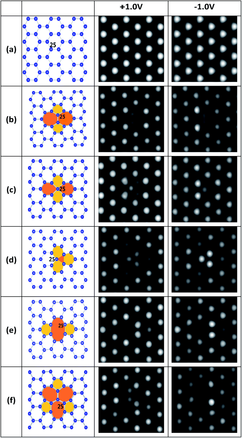 | ||
| Fig. 1 Geometric structures (left plots) and their simulated STM images (right two plots) of perfect and defective stanene at ±1.0 V bias: (a) pristine; (b) SW; (c) SV-1(55|66); (d) SV-2(3|555); (e) DV-1(5|8|5); (f) DV-2(555|777). | ||
To further study the probability of formation and thermodynamic stability of these defects, we computed their formation energies and listed them in Table 1, as well as the values of those in graphene and silicene sheet from the literature33,37–39,54–56 for comparison. Apparently, the formation energies (1.21–1.80 eV) of all these defects in stanene are lower than those in graphene (4.5–8.7 eV) and silicene (2.09–3.77 eV). This is resulted from the fact that binding energy of stanene is smaller (EB = 3.40 eV for stanene vs. EB = 7.90 eV for graphene and EB = 3.96 eV for silicene). Thus, these point defects could be more easily formed in stanene than those in graphene and silicene.
| EB | SW | SV-1 | SV-2 | DV-1 | DV-2 | |
|---|---|---|---|---|---|---|
| Stanene | 3.40 | 1.21 | 1.58 | 1.58 | 1.75 | 1.80 |
| Graphene | 7.9 [ref. 55] | 4.5–5.3 [ref. 33] | 7.38–7.85 [ref. 33, 54 and 56] | — | 7.52–8.7 [ref. 33, 54 and 56] | 6.4–7.5 [ref. 33 and 56] |
| Silicene | 3.96 [ref. 37] | 1.64–2.09 [ref. 37, 38 and 39] | 3.01 [ref. 37] | 3.77 [ref. 37] | 3.24–3.70 [ref. 37 and 39] | 2.74–2.84 [ref. 37 and 39] |
At a finite temperature T, the average equilibrium concentration of point defects in stanene follows the equation
| Ndefect/Nperfect = exp(−Ef/kBT) | (2) |
A local SW defect is formed by a Sn–Sn bond rotation of 90°, as depicted in Fig. 1b. The STM images of SW in stanene are difficult to correlate with the atomic structure, since the defect atoms in different planes are very different from those of graphene showing easier-to-understand STM images.33 Because the two rotation atoms are located in the middle plane of the buckling stanene sheet, two local medium bright spots with a distance of about 2.72 Å can be observed in the STM image.
SVs are very common defects in 2D materials and have been experimentally observed in graphene and silicene.12,13,32,40–44 Two types of SVs in stanene, SV-1(55|66) and SV-2(3|555), are shown in Fig. 1c and d, respectively. SV-1(55|66) includes a sp3 – hybridized central tin atom and our calculation shows that it has a formation energy 3 meV lower than SV-2(3|555) does. Interestingly, starting from removing one atom in pristine stanene, our optimization shows that in this way the most stable single vacancy in stanene is SV-2(3|555) defect, which has three bonding atoms. This is totally different from the most stable SV(5|9) defect in graphene, which has two atoms bonding together,33 or another kind of defect in silicene, which has three dangling atoms.37 The preference of SV-2(3|555) defect with three bonding atoms in stanene may be related to the bigger atomic number of tin atom and closer distance between the tin atoms. Since the formation energies of SV-1(55|66) and SV-2(3|555) are almost same (1.578 eV and 1.581 eV), both of them are the most stable SVs in the stanene, which is very different from those in graphene33 and silicene.37 As for their STM images, SV-1(55|66) is somewhat alike to a SW defect, which has one atom at the mid plane of the buckling stanene sheet. SV-2(3|555) has three local gray atoms in the middle that are a little darker than those original bright atoms. Since one atom is lost, other three atoms around it move to the mid plane with a tiny distance.
There are two types of DVs in stanene, namely DV-1(5|8|5) in Fig. 1e and DV-2(555|777) in Fig. 1f. Both of the DVs can be formed from SVs, owning to a remarkable energy reduction of coalescence of two SVs: the formation energies for DV-1(5|8|5) and DV-2(555|777) are 1.75 eV and 1.80 eV, respectively, which are 1.41 eV and 1.36 eV lower than those of two isolated SVs, respectively. DV-1(5|8|5) is the initial structure after two SVs coalesce together, and DV-2(555|777) can be transformed from DV-1(5|8|5) by bond rotation.32,37,39,40,46 However, different from those in graphene and silicene,33,37 DV-2(555|777) in stanene is not a more energetically favored construction, whose formation energy is 0.05 eV higher than that of DV-1(5|8|5). Considering this tiny value of energy gain, there is still a great possibility to form a DV-2(555|777) defect. The STM image of DV-1(5|8|5) has four bright spots, indicating strongly localized electronic density around these defective atoms, similar to those of graphene and silicene.32,37 And for the image of DV-2(555|777), it can be distinguished by the three big heptagon at ±1.0 V bias and four medium bright atoms arrange in upright “Z” at −1.0 V in the STM image.
In summary, in comparison with graphene and silicene, the formation energies of point defects in stanene are lower. The case of SW in stanene is similar to that of graphene and silicene. Both SV-1(55|66) and SV-2(3|555) are the most stable SVs in the stanene, different from the most stable SV(5|9) in graphene and SV-1(55|66) in silicene. Interestingly, DV-1(5|8|5) is more stable than DV-2(555|777), with a little lower formation energy about 50 meV, which is opposite to those in graphene and silicene.
B. Formation, diffusion and transformation of point defects
Atomic diffusion in 2D monolayer materials often happens, thus the point defects may form, aggregate, separate or transform at a finite temperature, which in nature is dominated by their kinetic diffusion barrier.37,46 In this section, to demonstrate the diffusion behaviors of typical point defects, we simulate the processes of a local SW defect taking shape from pristine stanene and an initial DV-1(5|8|5) defect changing into a DV-2(555|777) defect.The energy profile and the structural images along the diffusion path of a local SW defect forming process are plotted in Fig. 2a. A Sn–Sn bond (highlighted by yellow color) rotation makes the SW defect. The rotation energy barrier site (labeled as TS) is calculated for about 1.23 eV, lower than that in graphene (∼10 eV)33 and silicene (2.64 eV),37 implying a greater probability to get a local SW defect in stanene. It is noteworthy that the reverse barrier from SW back to pristine stanene is only about 0.02 eV, smaller than that in graphene and silicene likewise.33,37 Therefore, a pristine stanene would overcome 1.23 eV energy barrier and then become a local SW defective stanene; in turn, a SW defect is also easy to be recovered, due to the reverse transition barrier is as low as 0.02 eV. Based on this, we could speculate that the SW defect in stanene can be recovered by annealing at a suitable temperature experimentally.
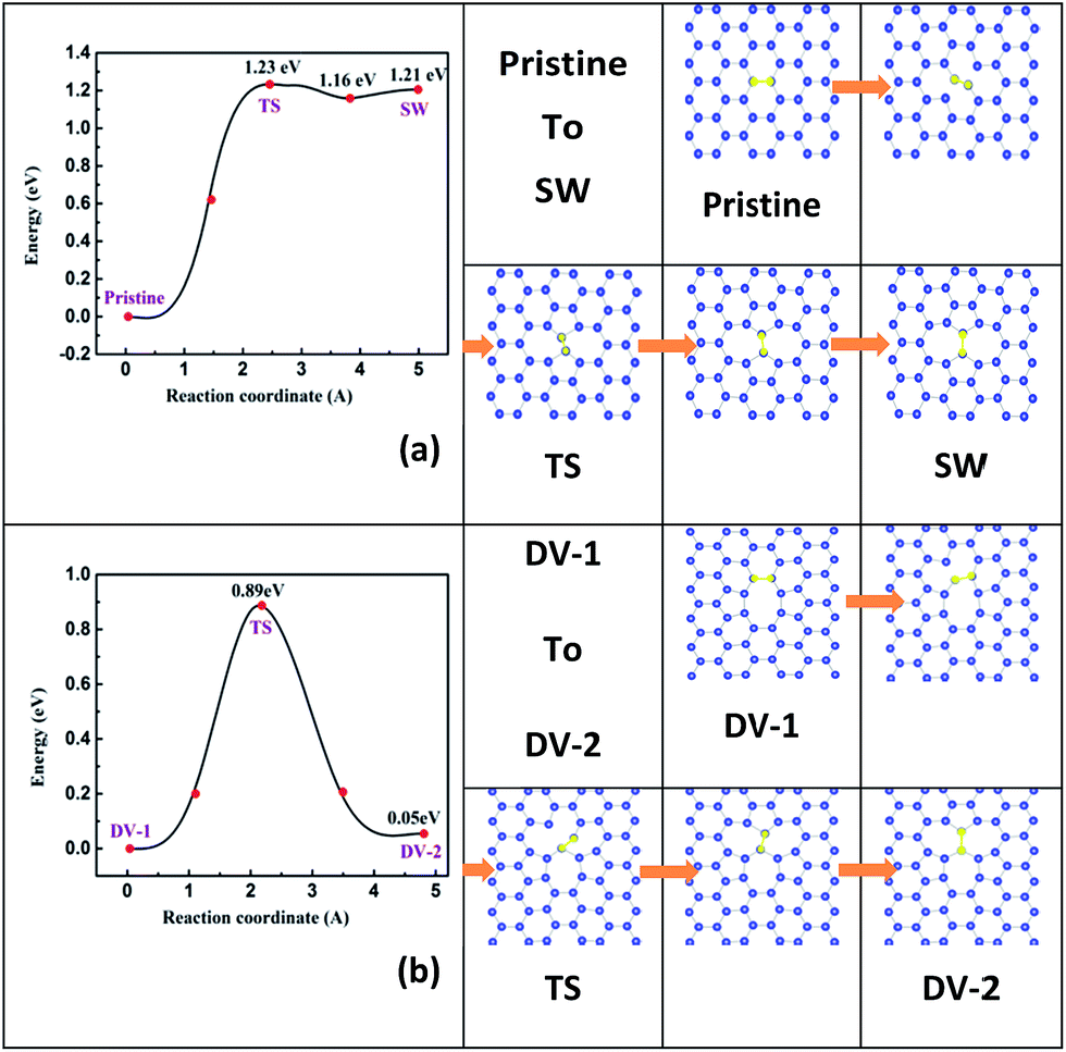 | ||
| Fig. 2 Energy barrier in diffusion path for (a) diffusion process from pristine stanene to SW defective stanene; and (b) from DV-1(5|8|5) to DV-2(555|777) defective stanene. Structural images along the diffusion path are plotted on the right panels. | ||
The detailed schema of a DV-1(5|8|5) turns to a DV-2(555|777) is shown in Fig. 2b. As mentioned before, DV-1(5|8|5) is the energetically favored site in stanene DVs, which is different from those in graphene and silicene.33,37 However, by climbing over a maximal barrier of 0.89 eV, DV-1(5|8|5) might diffuse to a DV-2(555|777). Furthermore, the energy difference between DV-2(555|777) and DV-1(5|8|5) is only about 0.05 eV. In a word, there is still some possibility of DV-2(555|777) arising in stanene at room temperature.
C. Electronic properties of defective stanene
The electronic band structure and partial charge density of the conduction band minimum (CBM) and valence band maximum (VBM) are showed in Fig. 3. The pristine stanene monolayer is shown in Fig. 3a. Two energy bands cross linearly at the K (and K′ = −K) point. Thus, stanene is a QSH insulator, similar to graphene. The π and π* band form the so-called “Dirac cone”.22 Notably, inclusion of SOC opens an 80.0 meV band gap at K point. It is well known that the existence of local defects do affect the electronic properties significantly in graphene and silicene.32 As well in stanene,49 the study of the local electronic properties of typical point defects is important for adopting a systematic way to create a picture of the defective stanene.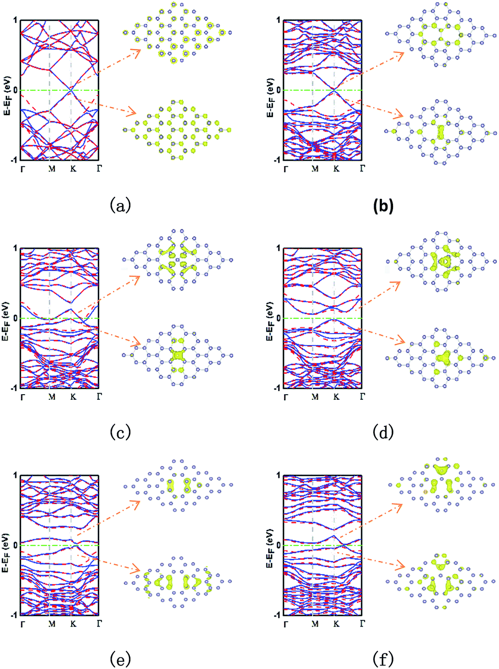 | ||
| Fig. 3 Electronic band structures (left) and partial charge density of CBM and VBM (right) of pristine and defective stanene: (a) pristine; (b) SW; (c) SV-1(55|66); (d) SV-2(3|555); (e) DV-1(5|8|5); (f) DV-2(555|777). The electronic band structures without SOC are plotted by blue solid curve and with SOC by red dash curve. | ||
Fig. 3b shows for the SW defect. In comparison with that of pristine stanene, the SW defect increases the band gap by a small value of about 20.2 meV through breaking the hexagonal symmetry, and this value is enlarged to 63.5 meV, when SOC is induced. It is interesting that the stanene with a SW defect almost retains the linear dispersion relationship near the Fermi level. Thus, we could presume that a stanene lattice with a small amount of SW defects can open a small gap with little harm to the high-velocity carriers. This result may have potentials of application in ultrafast microelectronic devices.
The stanene with SV-1(55|66) defect is metallic, whose band structure shows two mildly zigzag bands crossing the Fermi level presenting a strongly localized character, as shown in Fig. 3c. When it comes to SV-2(3|555), it also has a significant effect on the band structure of stanene, as shown in Fig. 3d. The three bonding atoms induce an indirect band gap between M point and K point about 77.4 meV (72.5 meV with SOC). Furthermore, the band at K point in VBM is similar to that in SW, but more localized.
In the case of DV-1(5|8|5), two nearly flat bands above and below the Fermi level bring a 30.8 meV (47.7 meV with SOC) indirect band gap at two points with a little distance between K point and Γ point, and completely destroy the Dirac point, as shown in Fig. 3e. Particularly, the band in VBM almost touches the Fermi level with just 4 meV short. As to the DV-2(555|777) (Fig. 3f), the band structure is similar to that in the case of SV-1(55|66), but slightly squashed and up shifted. One nearly flat band in VBM touches the Fermi level at a point between K point and Γ point and another band in CBM is above the Fermi level with 12.9 meV (19.8 meV with SOC) at same point, resulting in a direct band semiconductor. Meanwhile, the linear dispersion of pristine stanene at the Fermi level is disappeared. In general, SOC has visible influences on the electronic bands, specifically the band gaps, but does not change the band dispersions remarkably.
Moreover, the different phenomena of the STM images and configurations of electronic band can be understood by the projected density of states (PDOS) of some neighboring stanene atoms in perfect and defective stanene, as shown in Fig. 4. The selected neighboring stanene atoms are labeled in Fig. 1 with serial number of atoms. It is found that the energy bands nearby the Fermi level are mainly contributed by 5py orbitals of the atoms. For pristine stanene, the PDOS image is almost symmetrical, thus there are symmetrical bright spots in the STM images at −1.0 V bias (valence bands) and +1.0 V bias (conduction bands). And for defective stanene, the neighboring atoms around the defects almost all contribute to the valence bands and conduction bands, thus the neighboring atoms can be observed and recognized in STM images with both −1 V bias and +1 V bias. It is worth noting that the total DOS image is very similar between SV-1(55|66) and SV-2(3|555), as well as 5s, 5px and 5pz orbitals of selected atoms in PDOS, indicating that different electronic properties between two SVs are mainly due to the variations of influences from the 5py orbitals. In addition, when SOC is considered for calculating the total DOS of stanene around the Fermi level, there is little distinction between the calculation with SOC and without SOC, which is consistent with the inapparent influence of SOC on electronic band dispersions.
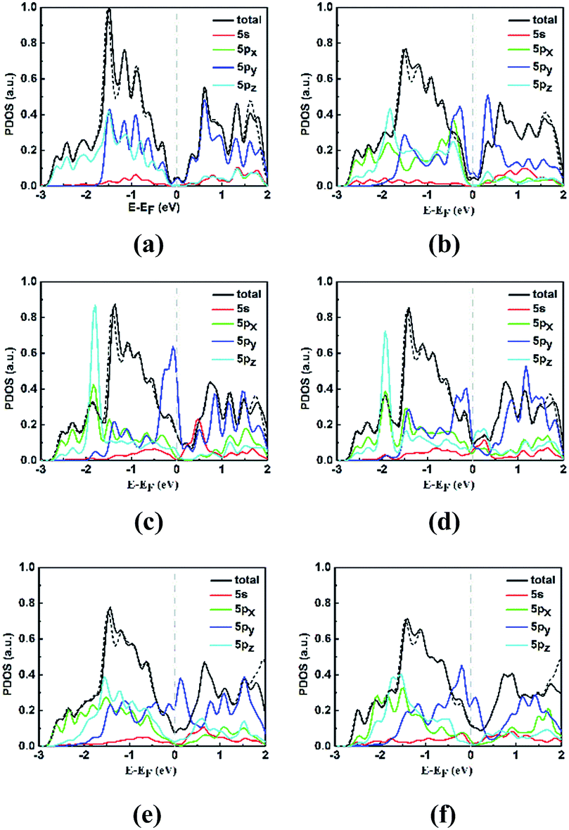 | ||
| Fig. 4 Projected density of states of pristine and defective stanene, black solid (dash) curve is for total density of states without SOC (with SOC) (reduced by one hundred times for view convenience), red, green, blue and cyan curve is for 5s, 5px, 5py and 5pz orbitals of selected atoms, respectively, all without SOC, and gray line indicates the Fermi level: (a) pristine; (b) SW; (c) SV-1(55|66); (d) SV-2(3|555); (e) DV-1(5|8|5); (f) DV-2(555|777). | ||
4. Conclusions
In this paper, we performed DFT calculations to investigate the structures and diffusion behaviors of several typical point defects and their influences on the electronic properties of stanene. Besides, the STM images were also simulated to help experimentalists identify these defects in stanene. The formation energies of these defects in stanene range from 1.21 eV to 1.80 eV, all lower than those in graphene and silicene. In the case of SVs, both SV-1(55|66) and SV-2(3|555) are the most stable ones in the stanene. As for DVs, the initial structure DV-1(5|8|5) can come from two SV-1(55|66)s coalesce together by releasing an energy of 1.41 eV, DV-2(555|777) can arise from a DV-1(5|8|5) via bond rotation by overcoming a barrier of 0.89 eV. Generation of a SW defect need to overcome an energy barrier of 1.23 eV, however it may be easily eliminated by an inverse bond rotation with activation energy of only 0.02 eV. The point defects have obvious influences on the electronic properties of stanene sheets. SW defects can open a small direct gap about 20.2 meV in energy bands and still retain the high velocity of carriers of pristine stanene. SVs would turn the semimetallic stanene into a metal or a semiconductor with an indirect band gap. DV-1(5|8|5) may open an indirect gap about 13 meV. When it comes to DV-2(555|777), the band structure exhibits direct band gap semiconducting behavior, but not at K point. Besides, SOC effects influence the electronic properties of perfect and defective stanene, specifically the band gaps. Our theoretical calculation may supply insights into the identification of point defects in further experiments and the cognition of their effects on the electronic properties and potential applications of stanene.Acknowledgements
This work was supported by the Natural Science Foundation of China (NSFC) through grant number 51671137.Notes and references
- K. S. Novoselov, D. Jiang, F. Schedin, T. J. Booth, V. V. Khotkevich, S. V. Morozov and A. K. Geim, Proc. Natl. Acad. Sci. U. S. A., 2005, 102, 10451 CrossRef CAS PubMed.
- R. Mas-Balleste, C. Gomez-Navarro, J. Gomez-Herrero and F. Zamora, Nanoscale, 2011, 3, 20 RSC.
- M. Osada and T. Sasaki, Adv. Mater., 2012, 24, 210 CrossRef CAS PubMed.
- M. Xu, T. Liang, M. Shi and H. Chen, Chem. Rev., 2013, 113, 3766 CrossRef CAS PubMed.
- S. Lebègue, T. Björkman, M. Klintenberg, R. M. Nieminen and O. Eriksson, Phys. Rev. X, 2013, 3, 031002 Search PubMed.
- K. S. Novoselov, A. K. Geim, S. V. Morozov, D. Jiang, Y. Zhang, S. V. Dubonos, I. V. Grigorieva and A. A. Firsov, Science, 2004, 306, 666 CrossRef CAS PubMed.
- S. Cahangirov, M. Topsakal, E. Aktűrk, H. Şahin and S. Ciraci, Phys. Rev. Lett., 2009, 102, 236804 CrossRef CAS PubMed.
- K. Watanabe, T. Taniguchi and H. Kanda, Nat. Mater., 2004, 3, 404 CrossRef CAS PubMed.
- X. Yang, Y. Ding and J. Ni, Phys. Rev. B: Condens. Matter Mater. Phys., 2008, 77, 041402 CrossRef.
- H. Liu, A. T. Neal, Z. Zhu, Z. Luo, X. Xu, D. Tománek and P. D. Ye, ACS Nano, 2014, 8, 4033 CrossRef CAS PubMed.
- B. Radisavljevic, A. Radenovic, J. Brivio, V. Giacometti and A. Kis, Nat. Nanotechnol., 2011, 6, 147 CrossRef CAS PubMed.
- B. Feng, Z. Ding, S. Meng, Y. Yao, X. He, P. Cheng, L. Chen and K. Wu, Nano Lett., 2012, 12, 3507 CrossRef CAS PubMed.
- P. Vogt, P. De Padova, C. Quaresima, J. Avila, E. Frantzeskakis, M. C. Asensio, A. Resta, B. Ealet and G. Le Lay, Phys. Rev. Lett., 2012, 108, 155501 CrossRef PubMed.
- C.-L. Lin, R. Arafune, K. Kawahara, N. Tsukahara, E. Minamitani, Y. Kim, N. Takagi and M. Kawai, Appl. Phys. Express, 2012, 5, 045802 CrossRef.
- M. E. Dávila, L. Xian, S. Cahangirov, A. Rubio and G. Le Lay, New J. Phys., 2014, 16, 095002 CrossRef.
- E. Bianco, S. Butler, S. Jiang, O. D. Restrepo, W. Windl and J. E. Goldberger, ACS Nano, 2013, 7, 4414 CrossRef CAS PubMed.
- S. Jiang, S. Butler, E. Bianco, O. D. Restrepo, W. Windl and J. E. Goldberger, Nat. Commun., 2014, 5, 3389 Search PubMed.
- F. F. Zhu, W. J. Chen, Y. Xu, C. L. Gao, D. D. Guan, C. H. Liu, D. Qian, S. C. Zhang and J. F. Jia, Nat. Mater., 2015, 14, 1020 CrossRef CAS PubMed.
- J. Gao, G. Zhang and Y. W. Zhang, Sci. Rep., 2016, 6, 29107 CrossRef CAS PubMed.
- S. Balendhran, S. Walia, H. Nili, S. Sriram and M. Bhaskaran, Small, 2015, 11, 640 CrossRef CAS PubMed.
- B. v. d. Broek, M. Houssa, E. Scalise, G. Pourtois, V. V. Afanas‘ev and A. Stesmans, 2D Materials, 2014, 1, 021004 CrossRef.
- Y. Xu, B. Yan, H. J. Zhang, J. Wang, G. Xu, P. Tang, W. Duan and S. C. Zhang, Phys. Rev. Lett., 2013, 111, 136804 CrossRef PubMed.
- C. C. Liu, H. Jiang and Y. Yao, Phys. Rev. B: Condens. Matter Mater. Phys., 2011, 84, 195430 CrossRef.
- G. F. Zhang, Y. Li and C. Wu, Phys. Rev. B: Condens. Matter Mater. Phys., 2014, 90, 075114 CrossRef.
- H. Huang, Z. Wang, N. Luo, Z. Liu, R. Lü, J. Wu and W. Duan, Phys. Rev. B: Condens. Matter Mater. Phys., 2015, 92, 075138 CrossRef.
- Y. Xu, Z. Gan and S. C. Zhang, Phys. Rev. Lett., 2014, 112, 226801 CrossRef PubMed.
- J. Wang, Y. Xu and S.-C. Zhang, Phys. Rev. B: Condens. Matter Mater. Phys., 2014, 90, 054503 CrossRef.
- S. C. Wu, G. Shan and B. Yan, Phys. Rev. Lett., 2014, 113, 256401 CrossRef PubMed.
- T. Niu, M. Zhou, J. Zhang, Y. Feng and W. Chen, J. Am. Chem. Soc., 2013, 135, 8409 CrossRef CAS PubMed.
- H. S. Song, S. L. Li, H. Miyazaki, S. Sato, K. Hayashi, A. Yamada, N. Yokoyama and K. Tsukagoshi, Sci. Rep., 2012, 2, 337 CAS.
- H. P. Komsa, J. Kotakoski, S. Kurasch, O. Lehtinen, U. Kaiser and A. V. Krasheninnikov, Phys. Rev. Lett., 2012, 109, 035503 CrossRef PubMed.
- M. M. Ugeda, I. Brihuega, F. Hiebel, P. Mallet, J.-Y. Veuillen, J. M. Gómez-Rodríguez and F. Ynduráin, Phys. Rev. B: Condens. Matter Mater. Phys., 2012, 85, 121402 CrossRef.
- F. Banhart, J. Kotakoski and A. V. Krasheninnikov, ACS Nano, 2011, 5, 26 CrossRef CAS PubMed.
- J. H. Chen, L. Li, W. G. Cullen, E. D. Williams and M. S. Fuhrer, Nat. Phys., 2011, 7, 535 CrossRef CAS.
- J. Zhang, J. Zhao and J. Lu, ACS Nano, 2012, 6, 2704 CrossRef CAS PubMed.
- S. Li, Y. Wu, Y. Tu, Y. Wang, T. Jiang, W. Liu and Y. Zhao, Sci. Rep., 2015, 5, 7881 CrossRef PubMed.
- J. Gao, J. Zhang, H. Liu, Q. Zhang and J. Zhao, Nanoscale, 2013, 5, 9785 RSC.
- H. Sahin, J. Sivek, S. Li, B. Partoens and F. M. Peeters, Phys. Rev. B: Condens. Matter Mater. Phys., 2013, 88, 045434 CrossRef.
- S. Haldar, R. G. Amorim, B. Sanyal, R. H. Scheicher and A. R. Rocha, RSC Adv., 2016, 6, 6702 RSC.
- H. Liu, H. Feng, Y. Du, J. Chen, K. Wu and J. Zhao, 2D Materials, 2016, 3, 025034 CrossRef.
- J. C. Meyer, C. Kisielowski, R. Erni, M. D. Rossell, M. F. Crommie and A. Zettl, Nano Lett., 2008, 8, 3582 CrossRef CAS PubMed.
- M. H. Gass, U. Bangert, A. L. Bleloch, P. Wang, R. R. Nair and A. K. Geim, Nat. Nanotechnol., 2008, 3, 676 CrossRef CAS PubMed.
- J. Kotakoski, A. V. Krasheninnikov, U. Kaiser and J. C. Meyer, Phys. Rev. Lett., 2011, 106, 105505 CrossRef CAS PubMed.
- H. Jamgotchian, Y. Colignon, N. Hamzaoui, B. Ealet, J. Y. Hoarau, B. Aufray and J. P. Biberian, J. Phys.: Condens. Matter, 2012, 24, 172001 CrossRef CAS PubMed.
- J. Ma, D. Alfè, A. Michaelides and E. Wang, Phys. Rev. B: Condens. Matter Mater. Phys., 2009, 80, 033407 CrossRef.
- G. D. Lee, C. Z. Wang, E. Yoon, N. M. Hwang, D. Y. Kim and K. M. Ho, Phys. Rev. Lett., 2005, 95, 205501 CrossRef PubMed.
- P. O. Lehtinen, A. S. Foster, Y. Ma, A. V. Krasheninnikov and R. M. Nieminen, Phys. Rev. Lett., 2004, 93, 187202 CrossRef CAS PubMed.
- P. O. Lehtinen, A. S. Foster, A. Ayuela, A. Krasheninnikov, K. Nordlund and R. M. Nieminen, Phys. Rev. Lett., 2003, 91, 017202 CrossRef CAS PubMed.
- W. Xiong, C. Xia, T. Wang, J. Du, Y. Peng, X. Zhao and Y. Jia, Phys. Chem. Chem. Phys., 2016, 18, 28759 RSC.
- G. Kresse and J. Furthmüller, Comput. Mater. Sci., 1996, 6, 15 CrossRef CAS.
- P. E. Blöchl, Phys. Rev. B: Condens. Matter Mater. Phys., 1994, 50, 17953 CrossRef.
- J. P. Perdew, K. Burke and M. Ernzerhof, Phys. Rev. Lett., 1996, 77, 3865 CrossRef CAS PubMed.
- G. Henkelman, B. P. Uberuaga and H. Jónsson, J. Chem. Phys., 2000, 113, 9901 CrossRef CAS.
- H. Zhang, M. Zhao, X. Yang, H. Xia, X. Liu and Y. Xia, Diamond Relat. Mater., 2010, 19, 1240 CrossRef CAS.
- J. M. H. Kroes, M. A. Akhukov, J. H. Los, N. Pineau and A. Fasolino, Phys. Rev. B: Condens. Matter Mater. Phys., 2011, 83, 165411 CrossRef.
- J. Kotakoski, A. V. Krasheninnikov and K. Nordlund, Phys. Rev. B: Condens. Matter Mater. Phys., 2006, 74, 245420 CrossRef.
| This journal is © The Royal Society of Chemistry 2017 |