DOI:
10.1039/C6RA28074A
(Communication)
RSC Adv., 2017,
7, 5514-5518
Design and characterization of methoxy modified organic semiconductors based on phenyl[1]benzothieno[3,2-b][1]benzothiophene†
Received
12th December 2016
, Accepted 3rd January 2017
First published on 17th January 2017
Abstract
Two environmentally and thermally stable [1]benzothieno[3,2-b][1]benzothiophene (BTBT) derivatives, BOP-BTBT and DBOP-BTBT are successfully synthesized and analyzed as active layers in organic thin film transistors. The effects of methoxy on BTBT based OTFT materials are reported for the first time. The experimental results show an excellent optimization influence of methoxy group on the OTFT performance with an improved hole transport mobility up to 0.63 cm2 V−1 s−1 (BOP-BTBT) and 3.57 cm2 V−1 s−1 (DBOP-BTBT). Meantime the mono- and bis-substituted derivatives are compared in terms of their physical properties and device performance. We find that the threshold voltage decreases when more methoxy groups are introduced.
Introduction
Organic thin film transistors (OTFTs) have attracted much attention due to their potential applications in optoelectronic devices including sensors, electronic paper, transparent circuits and low-cost and flexible displays.1 In recent decades, enormous progress has been made in organic semiconductors (OSCs) and different kinds of OSCs with mobility exceeding 1 cm2 V−1 s−1, higher than that of amorphous silicon, have been developed.2 Among the most efficient OSCs, [1]benzothieno[3,2-b][1]benzothiophene (BTBT) derivatives show excellent OTFT performance because of the strong intermolecular interactions between sulfur atoms and large electron cloud overlap between OSC molecules. In 2006, BTBT core was used in organic semiconductors for the first time and diphenyl-substituted BTBT (DPh-BTBT) was synthesized. The highest charge mobility of DPh-BTBT achieved was 2.0 cm2 V−1 s−1 which was a dramatically high value at that time.3 In 2007, dialkyl-substituted BTBT was reported with good solubility in normal solvents. When the compound, R![[double bond, length as m-dash]](https://www.rsc.org/images/entities/char_e001.gif) C13H25 showed excellent performance in the solution processed OTFT devices with μ = 2.75 cm2 V−1 s−1 and Ion/Ioff > 107.4 Also in 2007, phenyl ring was fused to BTBT core and formed another star structure DNTT.5 Four years later, naphthyl-fused BTBT was reported called DATT6 and in 2012, mono functionalized BTBT using alkyl chain of C13H25 was studied and high hole mobility over 17.2 cm2 V−1 s−1 was attained by using AlOx/C14-PA as dielectric layer.7 In 2015, 2,7-di-tert-butyl-BTBT was reported as isotropic OTFT material with μ = 17 cm2 V−1 s−1 in single crystal FETs.8 Up to now, almost all BTBT derivatives are modified using alkyl chains and aromatic rings, however, the effect of hetero atoms on the BTBT derivatives is seldom studied.
C13H25 showed excellent performance in the solution processed OTFT devices with μ = 2.75 cm2 V−1 s−1 and Ion/Ioff > 107.4 Also in 2007, phenyl ring was fused to BTBT core and formed another star structure DNTT.5 Four years later, naphthyl-fused BTBT was reported called DATT6 and in 2012, mono functionalized BTBT using alkyl chain of C13H25 was studied and high hole mobility over 17.2 cm2 V−1 s−1 was attained by using AlOx/C14-PA as dielectric layer.7 In 2015, 2,7-di-tert-butyl-BTBT was reported as isotropic OTFT material with μ = 17 cm2 V−1 s−1 in single crystal FETs.8 Up to now, almost all BTBT derivatives are modified using alkyl chains and aromatic rings, however, the effect of hetero atoms on the BTBT derivatives is seldom studied.
BTBT derivatives usually exhibit good air stability due to the low lying highest occupied molecular orbital (HOMO) energy levels. For example, the HOMO level of DPh-BTBT is −5.6 eV.9 Meanwhile, the large difference between the HOMO level of OSCs and the work function of normally used gold source electrode (−5.1 eV) results in an obvious contact resistance between the active layer and the electrode which limits the OTFT device performance, especially in the linear region.10 In order to explore the effects generated by heteroatoms on BTBT derivatives and reduce the contact resistance in relevant devices, electron-donating methoxy group is introduced into phenyl-substituted BTBT. In our previous work,11 we introduced methoxy group into diphenyl-substituted anthracene to obtain high mobility (2.96 cm2 V−1 s−1) semiconductor along with strong fluorescence and isotropic properties. The designed target material is also expected to have excellent isotropic properties.
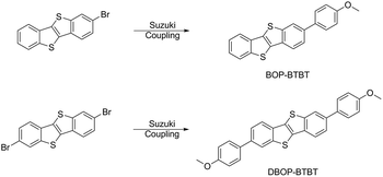
Herein, we successfully synthesize two novel materials, 2-(4-methoxyphenyl)benzo[b]benzo[4,5]thieno[2,3-d]thiophene (BOP-BTBT) and 2,7-bis(4-methoxyphenyl)benzo[b]benzo[4,5]thieno[2,3-d]thiophene (DBOP-BTBT) by Suzuki coupling. Optical and electrical properties of BOP-BTBT and DBOP-BTBT are measured and OTFT devices based on these two materials are successfully fabricated and tested. All the devices show apparently improved FETs performance compared to the phenyl-substituted ones, with an increase in mobility from 0.02 cm2 V−1 s−1 (Ph-BTBT)12 to 0.63 cm2 V−1 s−1 (BOP-BTBT) and from 2.0 cm2 V−1 s−1 (DPh-BTBT) to 3.57 cm2 V−1 s−1 (DBOP-BTBT). Meantime, we find that the threshold voltage decreases when more methoxy groups are introduced into the semiconductor structure.
Results and discussion
Synthesis
The aimed compound is synthesized through Suzuki–Miyaura coupling reaction13 using (4-methoxyphenyl)boronic acid and bromo substituted [1]benzothieno[3,2-b]benzothiophene (BTBT).14 The later one was obtained according to the reported procedure15 (details in ESI†). The coupling reaction mixture was purified through vacuum sublimation three times at 260 °C for BOP-BTBT and 290 °C for DBOP-BTBT, to get pure materials as white powder and pale-yellow powder respectively. Finally, the chemical structures were confirmed by NMR and MS (ESI†). While the DBOP-BTBT was too hard to dissolve, so we used elemental analysis and single crystal X-ray analysis to confirm the structure.
Thermal and photo physical properties
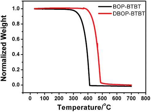
As shown in Fig. 1, BOP-BTBT and DBOP-BTBT exhibit good thermal stability with 5% weight loss at temperatures of 325 °C and 415 °C, respectively, as measured by thermogravimetric analysis (TGA). The bis-substituted derivative is more thermally stable than the mono-substituted derivative. This high decomposition temperature ensures potential OTFT availability under high temperature conditions.
 |
| | Fig. 1 TGA plots of BOP-BTBT and DBOP-BTBT in nitrogen with a heating rate of 10 °C min−1. | |
Thin films of BOP-BTBT and DBOP-BTBT with a thickness of ∼50 nm were vacuum-deposited on quartz substrates for measurement of UV-vis absorption spectra (Fig. 2). BOP-BTBT and DBOP-BTBT exhibit an absorption onset of 400 nm and 420 nm in solid state, respectively, which shows an apparent absorption red-shift compared to that in dichloromethane solution (360 nm and 382 nm). This indicates the strong intermolecular interactions in the thin films. The optical HOMO–LUMO gaps estimated from the absorption edge in thin films are 3.10 eV (BOP-BTBT) and 2.95 eV (DBOP-BTBT). The optical band gap of DBOP-BTBT is narrowed as compared to that of BOP-BTBT, which is consistent with the introduction of electron donating methoxy phenyl units. Based on the calibration of redox potentials of an internal ferrocene reference (Fc/Fc+), the thermally evaporated thin films of the two materials on GCE electrode were subjected to cyclic voltammetry (CV) (Fig. 2). The cyclic voltammetry of DBOP-BTBT in acetonitrile shows onset of the first oxidation potential at +0.69 V vs. Fc/Fc+, corresponding to HOMO energy level of −5.49 eV,16 which is 0.11 eV higher than that of the reported DPh-BTBT (HOMO = −5.6 eV). The results are summarized in Table 1.
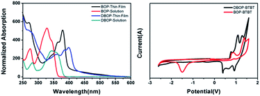 |
| | Fig. 2 The UV-vis absorption spectra and cyclic voltammogram of BOP-BTBT and DBOP-BTBT. | |
Table 1 Electrochemical and optical properties of BOP-BTBT and DBOP-BTBT
| |
E[ox]a (V) |
EHOMOb (eV) |
λtc (nm) |
λsd (nm) |
Ege (eV) |
| Estimated from electrochemical determination versus Fc/Fc+. EHOMO = −(E[onset,ox vs. Fc/Fc+] + 5.1) (eV). Estimated from thin film absorption spectra. Solution absorption spectra in dichloromethane. Energy band gap calculated from the absorption edge of the thin-film. |
| BOP-BTBT |
+0.73 |
−5.53 |
400 |
360 |
3.10 |
| DBOP-BTBT |
+0.69 |
−5.49 |
420 |
382 |
2.95 |
Charge transport properties
To investigate and compare the field-effect properties of the two materials, BOP-BTBT and DBOP-BTBT, organic thin-film transistors with top contact/bottom gate configuration were fabricated by vacuum deposition. The heavily doped silicon wafers with oxide thickness of 300 nm were firstly cleaned with the acetone, deionized water and isopropanol in the ultrasonic bath for 15 minutes, respectively. These substrates were then blown dry with nitrogen gas and further cleaned in oxygen plasma for 15 min. They were then treated in 0.03 g mL−1 concentration of octadecyl trichlorosilane (OTS) solution in toluene at 60 °C for 20 min to form self-assembled monolayer. The OTS-modified SiO2/Si substrates were rinsed with fresh toluene in the sonic bath for 1 min and blown dry with nitrogen gas. The organic active layer was then evaporated onto these substrates to a thickness of approximately 50 nm under the pressure of 1 × 10⁻⁴ Pa for each substrate temperature condition. Gold source and drain electrodes (W/L = 10) were deposited on the organic active layer using a shadow mask. Electrical characteristics of the OTFT devices were measured by Agilent B1500A in the ambient air. The hole mobility (μh) was obtained from the saturation regime using the following equation:
| Ids = Ciμe(W/2L)(Vg − Vth)2 |
In the above equation, Ids, W, L, Vg, Vth and Ci represent the drain-source current, channel width, channel length, gate voltage, threshold voltage and the capacitance per unit area of the gate dielectric layer, respectively.
We tried different substrate temperatures for BOP-BTBT (RT, 60 °C) and DBOP-BTBT (RT, 60 °C, 80 °C, 100 °C, 120 °C). Table 2 summarizes the performance of the thin film transistors fabricated at different substrate temperatures (Tsub).
Table 2 Experimental characteristics of polycrystalline thin film device at different substrate temperatures. All the data are reported in average values from more than 10 devices
| |
Tsub/°C |
Mobility/cm2 V−1 s−1 |
Ion/Ioff |
Average Vth/V |
| DBOP-BTBT |
RT |
0.54–0.68 |
>106 |
−11.4 |
| 60 |
0.66–0.72 |
>106 |
−20.8 |
| 100 |
2.92–3.57 |
>107 |
−25.3 |
| 120 |
1.81–2.15 |
>106 |
−32.2 |
| BOP-BTBT |
RT |
0.51–0.63 |
>106 |
−32.6 |
| 60 |
0.18–0.35 |
>106 |
−35.8 |
The output curves show standard linear and saturation regions. While the feature of injection barriers is not observed in the low-VD region. According to the table, DBOP-BTBT shows better overall OTFT performance than BOP-BTBT, especially at elevated substrate temperatures. When Tsub = RT, mobility of BOP-BTBT and DBOP-BTBT is almost the same around 0.6 cm2 V−1 s−1, which is higher than Ph-BTBT (0.012 cm2 V−1 s−1)12 and DPh-BTBT (0.36 cm2 V−1 s−1). With Tsub increasing, mobility of DBOP-BTBT simultaneously increases up to 3.57 cm2 V−1 s−1 (at Tsub = 100 °C) while mobility of BOP-BTBT drops by half to only 0.28 (at Tsub = 60 °C). The highest mobility obtained from Ph-BTBT12 is only 0.016 cm2 V−1 s−1, an order of magnitude lower than that of BOP-BTBT. The highest hole mobility for DBOP-BTBT is 3.57 cm2 V−1 s−1 with Vth = −25.3 V and the relative Ion/Ioff = 2.13 × 10⁷. This mobility is almost two times higher than that reported for DPh-BTBT (2.0 cm2 V−1 s−1), which was obtained by addition of only two methoxy groups. Noticeably, the Vth of BOP-BTBT is much lower than that of Ph-BTBT (almost −50 V). Also, Vth of DBOP-BTBT (RT, −11.4 V) is lower than BOP-BTBT (RT, −32.6 V) (Fig. 3).
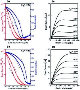 |
| | Fig. 3 Typical OTFT characteristics (transfer and output curves) for BOP-BTBT and DBOP-BTBT thin films grown on the OTS-modified SiO2/Si substrates. (a) and (b) represent BOP-BTBT devices at Tsub = RT. (c) and (d) represent DBOP-BTBT devices at Tsub = 100 °C. | |
Morphological characterizations
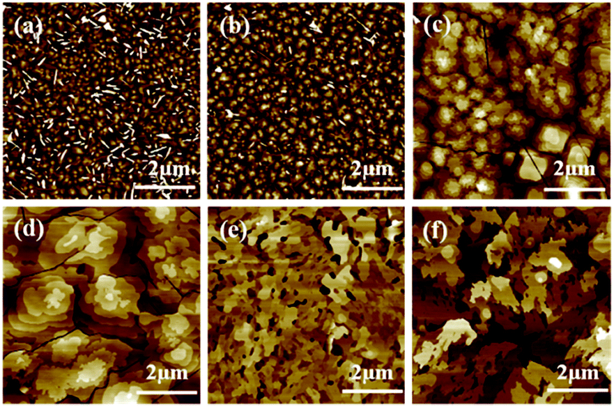
The OTFT performance is greatly affected by the substrate temperature through influencing the grain size, as shown in the atomic force microscopy (AFM) images in Fig. 4. For DBOP-BTBT, the polycrystalline domain size in the thin film deposited at room temperature is only 0.1 μm while the grain size grows to 1–1.5 μm in the films deposited at 100 °C. When DBOP-BTBT is deposited at 120 °C, we get larger but discontinuous polycrystals compared to those at 100 °C with the emergence of deep cracks, which explains the decrease of transistor performance. However, for BOP-BTBT, the polycrystalline domain size is only 0.3 μm at Tsub = RT, but when the substrate is merely heated to 60 °C the grains grow and morphology of the thin films becomes very chaotic which is the cause of the obvious decay in the relative performance of the OTFT devices.
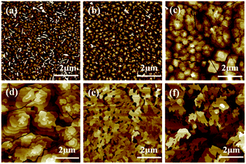 |
| | Fig. 4 AFM images (5 μm) of DBOP-BTBT (a–d) and BOP-BTBT (e and f) based polycrystalline thin-films on the OTS-modified SiO2/Si substrate at various substrate temperatures. (a) RT; (b) 60 °C; (c) 100 °C; (d) 120 °C; (e) RT; (f) 60 °C. | |
X-ray analysis
To investigate the molecular packing, single crystals of DBOP-BTBT (CCDC 1518254) with sufficient quality for X-ray structural analysis were grown by vacuum sublimation under 10−5 Pa. But for BOP-BTBT, sublimation could not form large enough crystals for X-ray structural analysis. Also, the method of slow evaporation of solvents (benzene, chlorobenzene, chloroform) tend to give out twin crystals which could not be used.
Single-crystal X-ray analysis of DBOP-BTBT demonstrate that the compound exhibits a typical herringbone packing structure with crystal parameters of: a = 7.5863 Å, b = 6.0552 Å, c = 46.173 Å and α = β = γ = 90°. The intermolecular distance between two adjacent DBOP-BTBT molecules along the π-stacking direction is only 6.06 Å (6.19 Å for DNTT). The torsion angle of phenyl rings out of BTBT core planes is measured to be 14.75° which indicates an almost planar structure of DBOP-BTBT. Two main kinds of sulfur–sulfur van der Waals interactions exist in a–b plane and the distance between sulfur atoms is 3.40 Å and 3.77 Å. Also, the methoxy group causes strong contacts between O and H with a distance of 2.582 Å between oxygen and hydrogen atoms. This flat molecular structure and multi strong intermolecular interactions lead to dense packing of DBOP-BTBT and higher mobility compared to that reported for DPh-BTBT (Fig. 5).
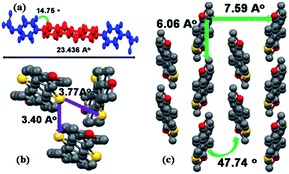 |
| | Fig. 5 Single crystal structure of DBOP-BTBT. (a) Molecular length and torsion angle. (b) Two types of S–S contacts. (c) Herringbone packing. | |
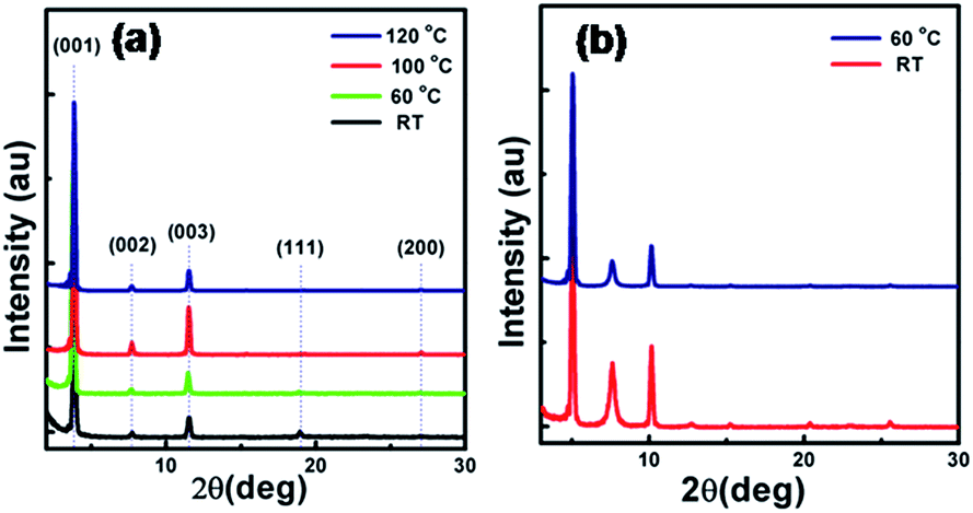
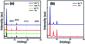
As shown in Fig. 6, the X-ray diffraction (XRD) measurements of the BOP-BTBT and DBOP-BTBT thin films on Si/SiO2 substrates show a series of peaks assignable to (00h) reflections. For DBOP-BTBT, a primary diffraction peak appears at 2θ = 3.80°, with fourth diffraction peak at 2θ = 7.73° and sixth diffraction peak at 2θ = 11.50°. The d-spacing of DBOP-BTBT obtained from the first reflection peak is 23.22 Å, which is very close to the length of DBOP-BTBT molecule (23.436 Å), indicating that DBOP-BTBT molecules are grown perpendicular to the substrate. This inference is further confirmed by the step height of the 2 μm thin film terraces which is 23.11 Å, as shown in Fig. 7. For BOP-BTBT, primary diffraction peak appears at 2θ = 2.53°, indicating that the d-spacing of BOP-BTBT is 34.91 Å, which is much larger than that of DBOP-BTBT. Compared to thin films deposited at room temperature, thin films at 60 °C display stronger diffraction peaks. This reveals that the crystal quality of thin films drops with the increase of substrate temperature.
 |
| | Fig. 6 XRD pattern of the thin films of (b) BOP-BTBT and (a) DBOP-BTBT as deposited at various substrate temperatures. | |
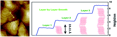 |
| | Fig. 7 The step heights of crystalline terrace layers as measured along the line marked in left and DBOP-BTBT layer-by-layer packing mode in the films. | |
Conclusions
Two environmentally and thermally stable BTBT derivatives BOP-BTBT and DBOP-BTBT are designed and synthesized. This is the first time that methoxy group is introduced into BTBT core. All of the devices show apparently improved FETs performance compared to those based on the phenyl-substituted molecules. An improvement in the mobility from 0.02 cm2 V−1 s−1 (Ph-BTBT) to 0.63 cm2 V−1 s−1 (BOP-BTBT) and from 2.0 cm2 V−1 s−1 (DPh-BTBT) to 3.57 cm2 V−1 s−1 (DBOP-BTBT) has been demonstrated in the fabricated OTFTs. Meantime, through the comparison of derivatives containing different numbers of methoxy group, we find that the threshold voltage decreases with more methoxy groups. Photophysical, morphological and single crystal characterizations explain that the methoxy groups improve the charge transport performance by affecting the HOMO level and intermolecular interactions. The method of introducing methoxy groups into organic semiconductor structures could be a promising molecular design strategy.
Experimental section
General
All chemicals and solvents were analytical reagents unless otherwise noted. All of the reactions were performed under a nitrogen atmosphere in dry solvent. The synthetic route of BOP-BTBT and DBOP-BTBT is shown Scheme 1. Thermo-gravimetric analysis (TGA) was carried out on a TA Instruments TA2950 TGA system at a heating rate of 10 °C min−1 and a nitrogen flow rate of 60 cm3 min−1. Differential scanning calorimetry (DSC) was run on a TA Instrument DSC Q1000 at a heating or cooling rate of 5 °C min−1 under a nitrogen flow. XRD patterns were recorded using a Bruker D8 advance X-ray diffractometer with a Cu Kα source (λ = 1.541 Å). Film morphology was studied with atomic force microscopy (AFM) on a SPA400HV instrument with a SPI 3800 controller (Seiko Instruments).
 |
| | Scheme 1 Synthetic route to BOP-BTBT and DBOP-BTBT. | |
BOP-BTBT. To a 100 mL flask, 1.6 g (5 mmol) 2-bromo-BTBT, 1.28 g (10 mmol) 4-methoxyphenyl boronic acid and Pd(PPh3)4 200 mg was added under nitrogen. Then 15 mL ethanol, 40 mL toluene and 10 mL 2 M K2CO3 aqueous solution was added. The whole system was heated to 120 °C and kept overnight. Then the whole system was cooled down and 50 mL methanol was added. After filtration, the filtrate was washed with water and methanol successively, then dried under vacuum and further purified by sublimation. BOP-BTBT was obtained as a white solid with a yield of 65% (1.12 g). 1H NMR (400 MHz, CDCl3) δ 8.10 (d, 1H), 7.99–7.87 (m, 3H), 7.72–7.66 (m, 3H), 7.52–7.39 (m, 2H), 7.05 (d, 2H), 3.90 (s, 3H).
DBOP-BTBT. This was achieved in the same manner as the synthesis of BOP-BTBT. DBOP-BTBT was obtained as a yellow solid with a yield of 52% (1.4 g). Anal. calcd for C28H20O2S2: C, 74.31; H, 4.45; O, 7.07; S, 14.17. Found: C, 74.22; H, 4.47; S, 14.31.
Acknowledgements
This work was financially supported by the Shenzhen Peacock Program (KQTD2014062714543296), National Natural Science Foundation of China (Grant No. 51603003), Shenzhen Key Laboratory of Organic Optoelectromagnetic Functional Materials of Shenzhen Science and Technology Plan (ZDSYS20140509094114164), Shenzhen Science and Technology Research Grant (JCYJ20140509093817690), Nanshan Innovation Agency Grant (No. KC2015ZDYF0016A), Guangdong Key Research Project (No. 2014B090914003, 2015B090914002), Guangdong Talents Project, National Basic Research Program of China (973 Program, No. 2015CB856500), China Postdoctoral Science Foundation (2015M570892), Natural Science Foundation of Guangdong Province (2014A030313800) and Guangdong Academician Workstation (2013B090400016), Shenzhen Science and Technology Research Grant (JCYJ20160510144254604).
Notes and references
- G. Gelinck, P. Heremans, K. Nomoto and T. D. Anthopoulos, Organic Transistors in Optical Displays and Microelectronic Applications, Adv. Mater., 2010, 22, 3778–3798 CrossRef CAS PubMed.
- J. Mei, Y. Diao, A. L. Appleton, L. Fang and Z. Bao, Integrated Materials Design of Organic Semiconductors for Field-Effect Transistors, J. Am. Chem. Soc., 2013, 135, 6724–6746 CrossRef CAS PubMed.
- K. Takimiya, H. Ebata, K. Sakamoto, T. Izawa, T. Otsubo, T. Otsubo and Y. Kunugi, J. Am. Chem. Soc., 2006, 128(39), 12604–12605 CrossRef CAS PubMed.
- H. Ebata, T. Izawa, E. Miyazaki, K. Takimiya, M. Ikeda, H. Kuwabara and T. Yui, J. Am. Chem. Soc., 2007, 129(21), 15732–15733 CrossRef CAS PubMed.
- T. Yamamoto and K. Takimiya, Facile Synthesis of Highly π-Extended Heteroarenes, Dinaphtho[2,3-b:2′,3′-f]chalcogenopheno[3,2-b]chalcogenophenes, and Their Application to Field-Effect Transistors, J. Am. Chem. Soc., 2007, 129(8), 2224–2225 CrossRef CAS PubMed.
- K. Niimi, S. Shinamura and I. Osaka, et al., Dianthra[2,3-b:2′,3′-f]thieno[3,2-b]thiophene (DATT): Synthesis, Characterization, and FET Characteristics of New π-Extended Heteroarene with Eight Fused Aromatic Rings, J. Am. Chem. Soc., 2011, 133(22), 8732–8739 CrossRef CAS PubMed.
- A. Y. Amin, A. Khassanov and K. Reuter, et al., Low-voltage organic field effect transistors with a 2-tridecyl[1]benzothieno[3,2-b][1]benzothiophene semiconductor layer, J. Am. Chem. Soc., 2012, 134(40), 16548–16550 CrossRef CAS PubMed.
- S. Guillaume, L. Vincent and N. Claude, et al., Bulky end-capped [1]benzothieno[3,2-b]benzothiophenes: reaching high-mobility organic semiconductors by fine tuning of the crystalline solid-state order, Adv. Mater., 2015, 27(19), 3066–3072 CrossRef PubMed.
- H. Yagi, T. Miyazaki, Y. Tokumoto, Y. Aoki, M. Zenki, T. Zaima, S. Okita, T. Yamamoto, E. Miyazaki, K. Takimiya and S. Hino, Ultraviolet Photoelectron Spectra of 2,7-Diphenyl[1]benzothieno-[3,2-b][1]benzothiophene and Dinaphtho[2,3-b:2′,3′-f]thieno[3,2-b]-thiophene, Chem. Phys. Lett., 2013, 563, 55–57 CrossRef CAS.
- M. Kano, T. Minari and K. Tsukagoshi, Improvement of Subthreshold Current Transport by Contact Interface Modification in p-Type Organic Field-Effect Transistors, Appl. Phys. Lett., 2009, 94, 143304 CrossRef.
- L. Yan, Y. Zhao and H. Yu, et al., Influence of heteroatoms on the charge mobility of anthracene derivatives, J. Mater. Chem. C, 2016, 4(16), 3517–3522 RSC.
- Y. He, W. Xu and I. Murtaza, et al., Molecular Phase Engineering of Organic Semiconductors Based on [1]Benzothieno[3,2-b][1]benzothiophene Core, RSC Adv., 2016, 6, 95149–95155 RSC.
- J. Liu, H. Dong and Z. Wang, et al., Thin film field-effect transistors of 2,6-diphenyl anthracene (DPA), Chem. Commun., 2015, 51(59), 11777–11779 RSC.
- S. Y. Zherdeva, A. Barudi, A. Y. Zheltov and B. Stepanov, Zh. Org. Khim., 1980, 16, 430–438 CAS.
-
(a) M. Saito, I. Osaka, E. Miyazaki, K. Takimiya, H. Kuwabara and M. Ikeda, Tetrahedron Lett., 2011, 52(2), 285–288 CrossRef CAS;
(b) B. Košata, V. Kozmík and J. Svoboda, Collect. Czech. Chem. Commun., 2002, 67(5), 645–664 CrossRef;
(c) C. Niebel, Y. Kim, C. Ruzié, J. Karpinska, B. Chattopadhyay, G. Schweicher, A. Richard, V. Lemaur, Y. Olivier, J. Cornil, A. R. Kennedy, Y. Diao, W.-Y. Lee, S. Mannsfeld, Z. Bao and Y. H. Geerts, J. Mater. Chem. C, 2015, 3(3), 674–685 RSC;
(d) S. Inoue, H. Minemawari and J. Tsutsumi, et al., Effects of Substituted Alkyl Chain Length on Solution-Processable Layered Organic Semiconductor Crystals, Chem. Mater., 2015, 27(11), 3809–3812 CrossRef CAS.
- M. Cardona, W. Li, A. E. Kaifer, D. Stockdale and G. C. Bazan, Adv. Mater., 2011, 23(20), 2367–2371 CrossRef PubMed.
Footnote |
| † Electronic supplementary information (ESI) available. CCDC 1518254. For ESI and crystallographic data in CIF or other electronic format see DOI: 10.1039/c6ra28074a |
|
| This journal is © The Royal Society of Chemistry 2017 |
Click here to see how this site uses Cookies. View our privacy policy here. 
 Open Access Article
 This Open Access Article is licensed under a
  *ab
*ab