DOI:
10.1039/C6RA27906F
(Paper)
RSC Adv., 2017,
7, 22578-22586
Effect of erbium concentration on the structural, optical and electrical properties of a Bi4Ti3O12 system
Received
7th December 2016
, Accepted 20th April 2017
First published on 25th April 2017
Abstract
We have studied the influence of erbium doping on the optical and electrical properties of a Bi4Ti3O12 compound. Bi4−xErxTi3O12 (x = 0.0, 0.1, 0.2 and 0.3) samples are prepared by the solid state reaction method. X-ray diffraction (XRD) revealed that our samples are homogenous and crystallize in the orthorhombic system with the Fmmm space group. Absorbance measurement reveals that the peak intensity increases with increasing erbium concentrations and this behavior confirms the good homogeneity of the samples. DC-conductivity measurements show that all samples are characterized by a semiconductor behavior. It is found that electrical conductivity is reduced considerably with increasing erbium content up to x = 0.3. This is due to the decrease in oxygen vacancy density. For the free compound, dc-conductivity is characterized by the appearance of a saturation region at a specific temperature (Tsat = 480 K). For Er doped compounds, Tsat goes beyond 600 K. An AC-conductivity study shows that the conductivity is governed by the jump relaxation model (JRM) and conduction through grain boundaries. We found that the conductivity spectrum of the investigated materials obeys the Jonscher universal double power law. The deduced activation energy increases when increasing the erbium content from Ea = 467 meV for x = 0 to Ea = 670 meV for x = 0.3. Increasing the Er substitution reduces the frequency dispersion of the real part of the dielectric constant ε′. Also, the tan![[thin space (1/6-em)]](https://www.rsc.org/images/entities/char_2009.gif) δ plot indicates that the investigated samples exhibit the characteristics of a relaxor dielectric.
δ plot indicates that the investigated samples exhibit the characteristics of a relaxor dielectric.
1. Introduction
Recently, bismuth layer-structure ferroelectric (BLSF) materials have been attracting intensive attention from several research groups1–3 due to their high Curie temperatures (TC), exceptional thermal stability, excellent resistance to depolarization and fatigue, interesting crystal structures, strong anisotropic characters and peculiar electrical properties.4–6 Also, BLSF compounds are environmentally friendly and are lead (Pb) free. Such properties open up wide potential applications in the electronics industry which include the manufacture of memory devices, sensors, pyroelectric detectors, displays, switching devices, etc.7
The bismuth titanate Bi4Ti3O12 (BIT) is a BLSF element which generated special interest for light up-conversion, visible-light-driven photocatalytic and ferroelectric studies due to its excellent electrical, intensive optical properties and high stability under the harsh photocatalytic reaction conditions.8 BIT shows variety characteristics such as ferroelectric–paraelectric phase transition at the Curie temperature (TC) of 675 °C. Usually, it crystallizes in the polar orthorhombic system.9 The BIT exhibits an anisotropy in its ferroelectricity and electrical conduction which are depending on its structural properties.10 Many studies reported that bismuth titanate compounds have often been synthesized by adding or substitution element in order to ameliorate its electrical properties.11 The effect of introducing trivalent rare earth ions on the physical properties of diverses materials has been reported in the literature.12,13 Among these ions, erbium is found to be a good dopant which affects optical properties.14,15 Recently, it is found that erbium content modifies the electrical properties.3 It is noticed that the electrical properties show a continuous improvement with the increasing Er concentration. Such improvements in the electrical resistivity and reduction in dielectric losses are attributed to the suppression of the oxygen vacancy concentration. However, the correlation between optical and electrical properties is not investigated in detail. Accordingly, the present work presents the investigation of some physical properties of BIT ceramics. The latters have been doped with different erbium content in order to study their optical and electrical properties. Many techniques have been used for the preparation of BIT such as solid state reaction, sol–gel, hydrothermal, metal organic decomposition, coprecipitation and combustion.16–20 It is well known that the solid–state reaction method is expected to be a potential candidate for preparation ceramics materials which is easy to prepare. Using such method, Er doped BIT samples are elaborated. Then, we report in this paper, the effect of erbium doping on the structural, optical and electrical properties of Bi4Ti3O12 system.
2. Experimental details
The Bi4−xErxTi3O12 (x = 0.0, 0.1, 0.2 and 0.3) samples are synthesized using high purity precursors: Bi2O3, TiO2 and Er2O3 (purity > 99.9%) in the desired proportions. To prepare the samples, the conventional solid state reaction method at high temperature is used. The starting materials are weighted in the appropriate stoichiometric amounts then intimately mixed in an agate mortar. The powder is placed in an platinum crucible and calcined at 650 °C and 850 °C for 3 h. Then, the powder is mixed with 2 wt% polyvinyl alcohol (PVA) binder. The obtained product is pressed into pellets of about 1 mm of thickness. Pellets are sintered at 1050 °C for 3 h after various heat-treatments. The sample undergo several cycles of grinding–pelleting–sintering.21 Finally, these pellets are cooled from high temperature to room temperature following the cooling inertia of the furnace (∼8 h).22,23 A great care has been taken over the preparation method, the physical properties depend strongly on the synthesis route and also on the cooling method.
Structural characterizations are carried out by means of X-ray diffraction at room temperature utilizing a powder diffractometer using CuKα radiation (λ = 1.5406 Å). Scanning is performed at room temperature in the diffraction angle range between 2θ = 5° and 80° with a step size of 0.016°. Structural analysis is carried out with Rietveld analysis using Fullprof program.24,25 A scanning electron microscope (SEM) JEOL-JSM-5400 was used to observe the microstructure. Optical reflectance spectra of the films are obtained using an UV-Vis-NIR Shimadzu 3100 spectrophotometer equipped with an integrate sphere. A thin silver film is deposited through a circular mask of 6 mm of diameter on the both side of the pellet. A plane capacitor configuration is obtained and permits the investigation of electrical properties of the synthesized material. Measurements are conducted with an Agilent 4294A analyzer under vacuum and in dark with signal amplitude of 20 mV.
3. Results and discussion
3.1. X-ray diffraction
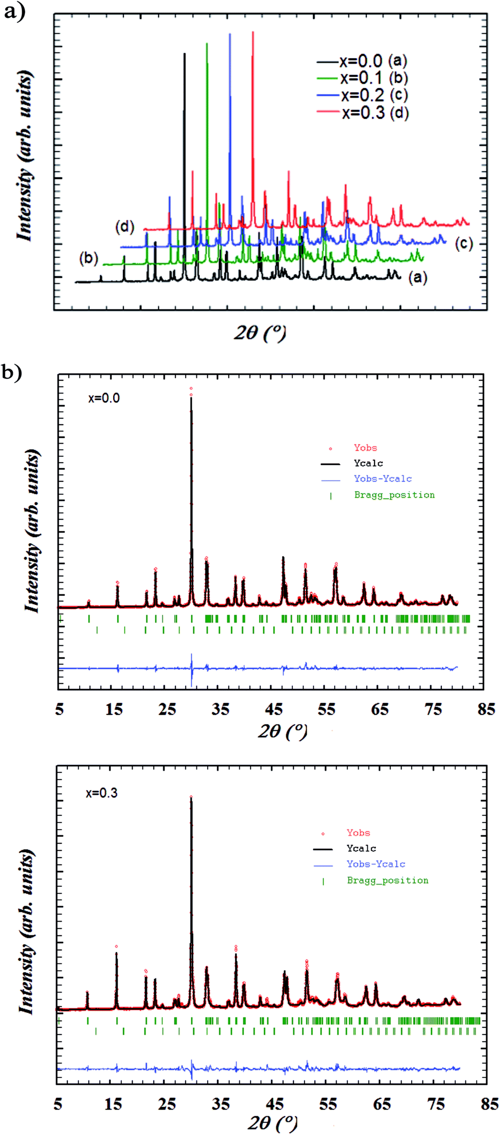
The Bi4−xErxTi3O12 with x = 0, 0.1, 0.2, and 0.3 samples are investigated by X-ray powder diffraction analysis. The XRD patterns of Bi4−xErxTi3O12 compounds registered at room temperature are depicted in Fig. 1a. The phase identification and structural analysis of samples are performed using the FullProf program24,25 and it is found that the samples are crystallized in the orthorhombic structure with Fmmm space group. These patterns reveal the presence of Bi2O3 peaks as the minor secondary phase with space group I23 in addition to the primary phase of Bi4−xErxTi3O12. This may be due to the mobility and segregation of particular bismuth at some places resulting in the formation of secondary phases during the process of calcination. This impurity is identified with X'Pert HighScore Plus software. Given the small concentration of the impurity, we assume that the secondary phase have a small influence on the microstructural development of Bi4−xErxTi3O12 system and have a little effect on the subsequent measurements of physical properties. This secondary phase will have no effect on electrical conductivity as it should be exist as isolated crystallites very spaced. It is important to note that the Bi2O3 is known as an excellent ionic conductor (with ρ ≈ 1 Ω cm at 1073 K26). Then, we investigate the electrical properties in the temperature range 80–700 K. Consequently, in this temperature range, the contribution of the impurity on the conductivity can be neglected. The structural refinement patterns including the observed and calculated profiles as well as the difference profile for the end members, Bi4Ti3O12 and Bi3.7Er0.3Ti3O12, are depicted in Fig. 1. The calculated XRD patterns coincide with the observed patterns as shown in Fig. 1b and c. Summary of structural parameters and the unit cell values obtained for each sample are listed in Table 1. Due to the smaller ionic radius of erbium (0.88 Å) as compared to bismuth (1.03 Å), the unit cell should monotonically decreases. But, in this study, it is observed that the lattice parameters and the unit cell did not show significant monotonic changes. The observed results indicates that the presence of the impurity corroborate the influence of the secondary phase on the structural parameters.
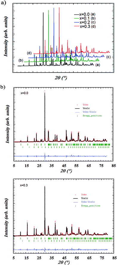 |
| | Fig. 1 (a) XRD patterns of Bi4−xErxTi3O12 ceramics with (0.0 ≤ x ≤ 0.3). (b) X-ray powder diffraction patterns and refinement at room temperature for: (i) x = 0.0 and (ii) x = 0.3. | |
Table 1 Structural data obtained after Rietveld refinement for Bi4−xErxTi3O12 (with 0.0 ≤ x ≤ 0.3)
| compound |
Symmetry |
a (Å) |
b (Å) |
c (Å) |
V (Å)3 |
| x = 0.0 |
Fmmm – orthorhombic |
5.409(1) |
5.446(4) |
32.819(4) |
966.869(1) |
| x = 0.1 |
Fmmm – orthorhombic |
5.410(6) |
5.447(8) |
32.831(7) |
967.745(1) |
| x = 0.2 |
Fmmm – orthorhombic |
5.406(1) |
5.441(1) |
32.809(2) |
965.078(9) |
| x = 0.3 |
Fmmm – orthorhombic |
5.405(9) |
5.442(4) |
32.821(3) |
965.627(7) |
3.2. SEM observations
The pellets used for optical measurements were observed by SEM and typical images are shown in Fig. 2. The white grains are from the residual BaSO4 (used in optical measurement) powder on the pellet surface. Otherwise, we note a compact compound with big size of grain elongated in one direction. This is due to the fact that the growth rate is higher in the direction perpendicular to the c-axis.27 No precipitates or secondary phase were observed. Each pellet was cleaved and the cross section was observed. The images of Fig. 3 show plate-like morphology for all samples. The plate-like grains have a large area, indicating good crystallinity, and are of random orientation.28 These images reveal also few pore and confirm the high density of the sample.
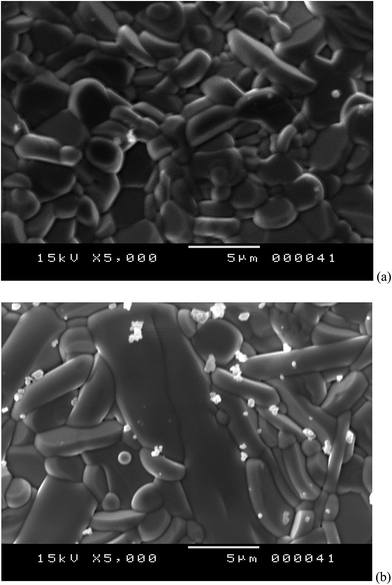 |
| | Fig. 2 SEM photographs of compounds with x = 0 and x = 0.2. | |
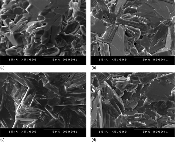 |
| | Fig. 3 Cross section morphology of the compounds obtained by SEM observation. | |
3.3. optical absorbance
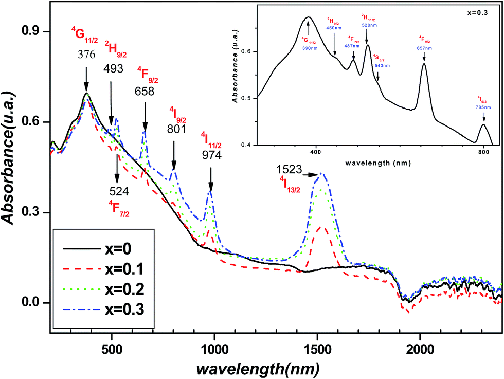
At room temperature, Fig. 4 shows the absorbance spectra, of the investigated compounds, in the range of wavelength between 200 and 2400 nm. For free erbium compound (x = 0.0), the absorbance increases when the wavelength increases from 200 to 376 nm, then, it decreases continually for the longer wavelength. When erbium is introduced several peaks appear in the spectra. These peaks correspond to the transition from the ground state 4I15/2 to excited one. Both positions and attribution, of each peak, are indicated in the Fig. 4 and its inset. The peaks are situated on 1530, 970, 795, 657, 543, 520, 487, 450 and 390 nm and are attributed to the transition to excited states 4I13/2, 4I11/2, 4I9/2, 4F9/2, 4S3/2, 2H11/2, 4F7/2, 2H9/2 and 4G11/2 respectively. Another peak should appear at 406 nm corresponding to the transition to the 4F5/2 state. But, its position is situated in the large absorbance band of the matrix and it can be identified. These obtained spectra are similar to those obtained by Zannen et al.29, in which the transition to 4I13/2 was not explored. The peak intensity increases with the increase of the erbium content. As these spectra are recorded at the same conditions, this behavior means that the peak intensity is correlated to erbium content. Thus, the evolution of the intensity with erbium content is another indicator of the good homogeneity of the samples.
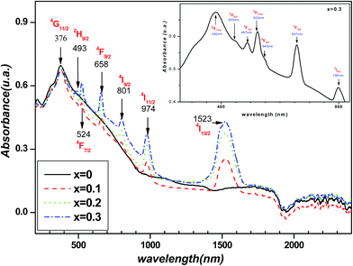 |
| | Fig. 4 Absorbance spectra of Bi4−xErxTi3O12 ceramics with (0.0 ≤ x ≤ 0.3). | |
3.4. AC conductivity
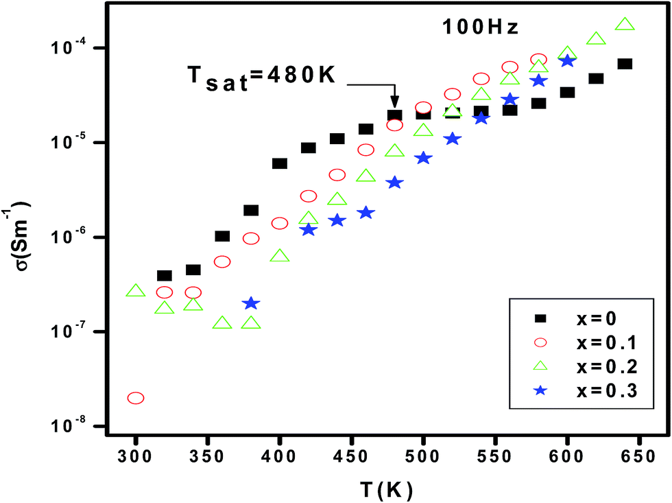
Fig. 5 shows the variation of the electrical conductivity versus temperature for different erbium concentrations. In the whole explored temperature range, Fig. 5 shows that dc-conductance increases with increasing temperature. Consequently, the material exhibits a semiconductor behavior. Also, the conductivity decreases when increasing erbium concentrations from x = 0.0 to x = 0.3 in the temperature range 300–480 K. In ferroelectric perovskite, the element substitution is related to the temperature dependence of conductivity. In such systems, oxygen vacancies are considered to be the most mobile charge carriers30 and mostly in titanates. At higher temperatures, oxygen vacancies will be ionized and release electron which contribute to the conduction. These electrons can be trapped by Ti3+ ions or oxygen vacancies and it can be thermally activated. The value of activation energy can help on distinguishing which trap is efficient. When erbium content increases, the oxygen vacancies are seen to be reduced. As continuous decrease is observed in the measured dc-conductivity for a change in Er content from x = 0.0 to 0.3. For the parent compound, the appearance of a saturation region, at Tsat = 480 K, is observed. When Er is introduced, the Tsat goes beyond the value 480 K. The rise on such specific temperature is related to several effects. In fact, the density of free carriers increases while increasing temperature. The carriers acquired a sufficient thermal energy to exceed the encountered barrier. In addition, the thermal activation contributes to a reduction of the efficiency of the capture of charge traps. At T > 480 K and for the erbium free compound, we suggest that the available density of trapped charge is vanished, then, the saturation region appear at higher temperature. The increase of Tsat increases with introducing erbium can be related to the trapping of charge carriers by defects created by erbium. So, a higher thermal energy is needed to release such carriers. Then, the conductivity increase again and the appearance of the saturation region is expected over the explored temperature range.
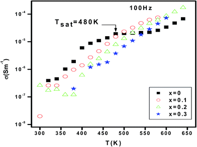 |
| | Fig. 5 Temperature dependence of dc-conductivity of Bi4−xErxTi3O12 ceramics with (0.0 ≤ x ≤ 0.3). | |
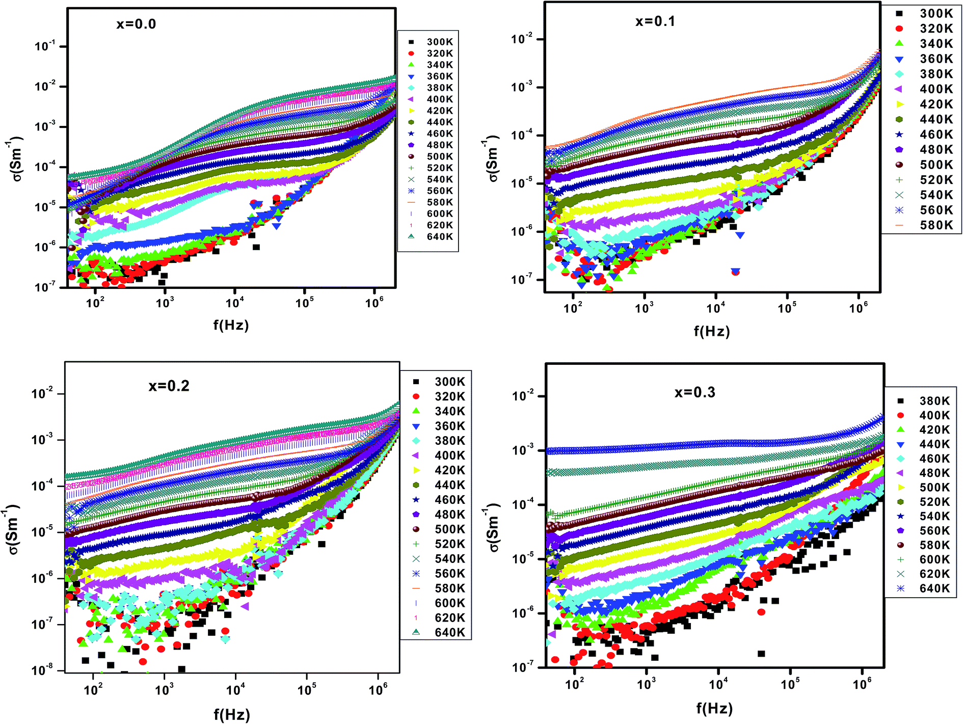
Fig. 6 shows the variation of conductivity versus frequency at different temperatures for x = 0.0, 0.1, 0.2 and 0.3. The conductivity spectrum possesses the following characteristics: (i) at low frequency, a plateau is observed and the conductivity increases with increasing temperature. Such observation indicates that conduction mechanism is thermally activated. (ii) At high temperature region, the conductivity plots are characterized by a change in the slope twice at low and high frequency. The variation of conductivity as a function of frequency is typical of a conductivity which is explained by the jump relaxation model (JRM)31 and conduction through grain boundaries.
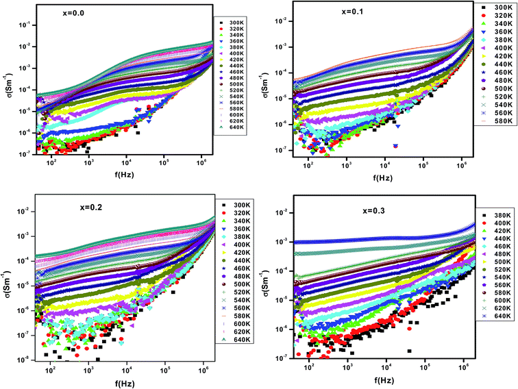 |
| | Fig. 6 Conductivity spectra of Bi4−xErxTi3O12 compounds with x = 0.0, 0.1, 0.2 and 0.3. | |
The JRM introduced by Funke and extended by Elliot,32 to account the ionic conduction in solids, is based on the existence of high probability for a jumping ion to jump back (unsuccessful hop). However, if the neighbourhood becomes relaxed with respect to the ion's position, the ion stays in the new site. In the low-frequency region, the conductivity is associated with successful hops. Beyond the low-frequency region, many hops are unsuccessful and as the frequency increases, more hops are unsuccessful. The change in the ratio of successful to unsuccessful hops results in dispersive conductivity. The JRM suggests that different activation energies are associated with unsuccessful and successful hopping processes. Applying JRM to the frequency response of ac conductivity, the experimental conductivity data are found to be described by the double power law proposed by Jonscher,33
where
σac is the total conductivity,
σdc is the transitional hopping, giving the long-range electrical transport in the long time limit. The coefficient (
A and
B) and the angular frequency exponent (
S1 and
S2) are temperature and material intrinsic property dependent constants
34,35
The dc conductivity is determined from the frequency independent region. Fig. 7 shows the variation of σdc against 1000/T. For oxide materials, the dc-conductivity is usually dependent upon the carrier concentration and mobility. At higher temperature, the conductivity follows the thermally activated transport of Arrhenius type described by the equation:
| σdc = σ0exp(Ea/kBT) |
where
σ0,
Ea, and
kB represent the pre-exponential term, the activation energy of the mobile charge carriers and Boltzmann's constant respectively. The activation energy is calculated from the linear portion of the plot of dc-conductivity
versus 1000/
T (
Fig. 7).
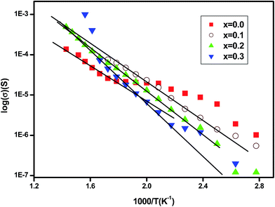 |
| | Fig. 7 Plot of log(σdc) vs. 1000/T. | |
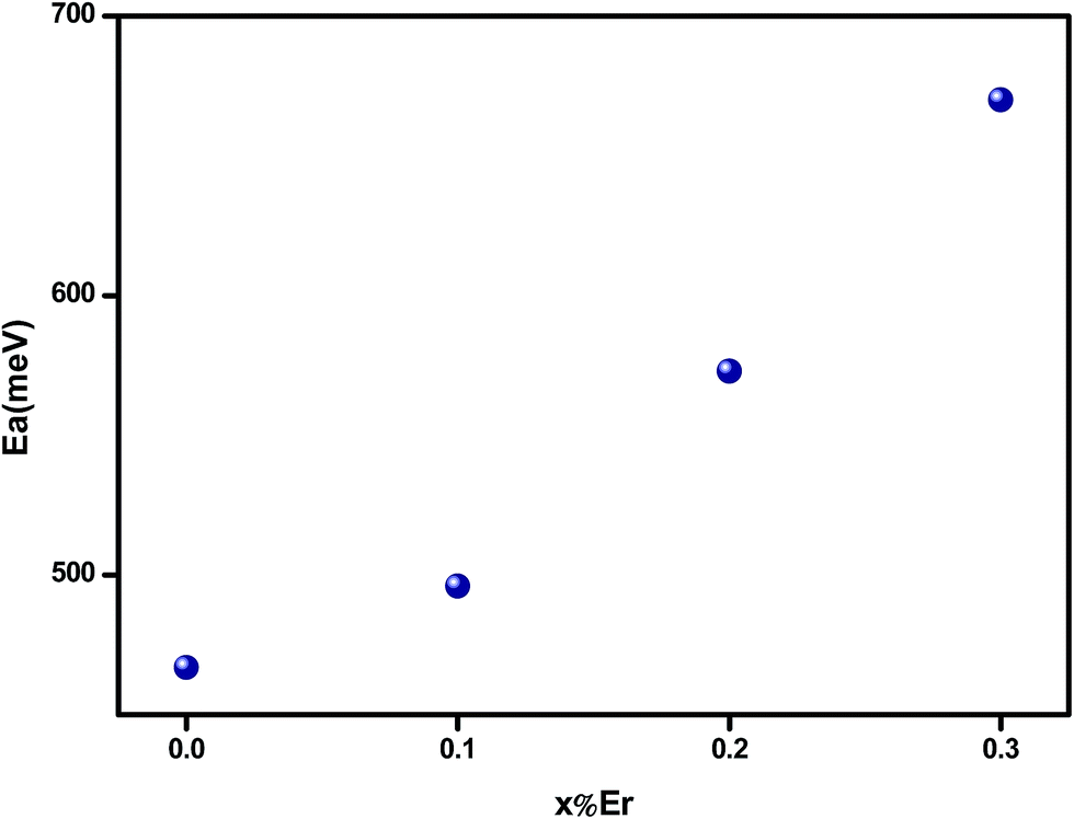
It is found that the activation energy increases with increasing erbium content as shown in Fig. 8. Thus, it can be assumed that the Er ion contributes indirectly in electrical conductivity. In ferroelectric perovskite,30 at higher temperature, the ionization of oxygen vacancies creates conducting electrons which are easily thermally activated. The large values of activation energy and conductivity evolution suggest that the conduction at higher temperature region, for charge carriers, may be oxygen vacancies.36 The rise in activation energy can be related to the reduction on motivating the oxygen vacancies jumping.1
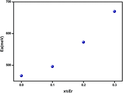 |
| | Fig. 8 Activation energy value for different erbium content. | |
3.5. Dielectric properties
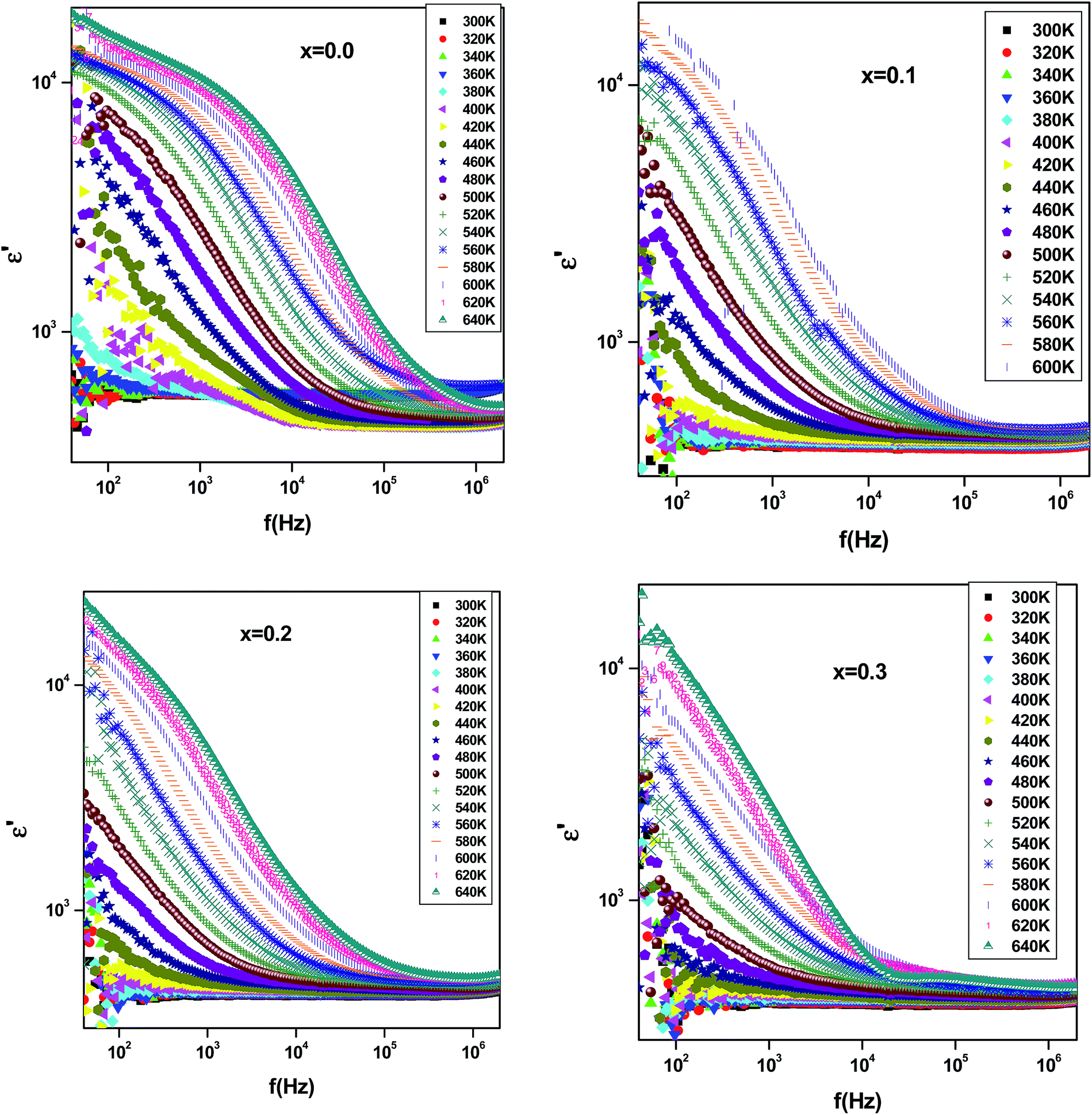
In order to study the effect of substitution with erbium ion on dielectric properties, the variation of dielectric constant ε′ as a function of frequency, for all investigated samples, is shown in Fig. 9. It is observed that dielectric constant decreases with increasing frequency. Such behavior can be related to the contribution of different polarization types (interfacial, dipolar, atomic, ionic, and electronic).37,38 At high frequency region, only dipolar and space charge polarization contribute to polarization leading to a decrease of the dielectric constant. At low frequency, the increase of the dielectric constant can be explained according to the Maxwell–Wagner polarization effect.39,40
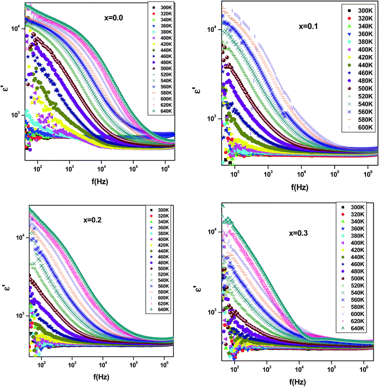 |
| | Fig. 9 Variation of dielectric constant (ε′) with frequency and temperature of Bi4−xErxTi3O12 ceramics with (0.0 ≤ x ≤ 0.3). | |
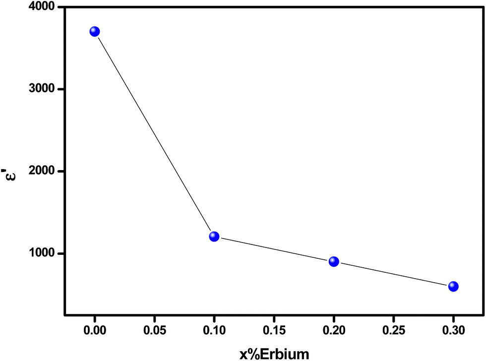
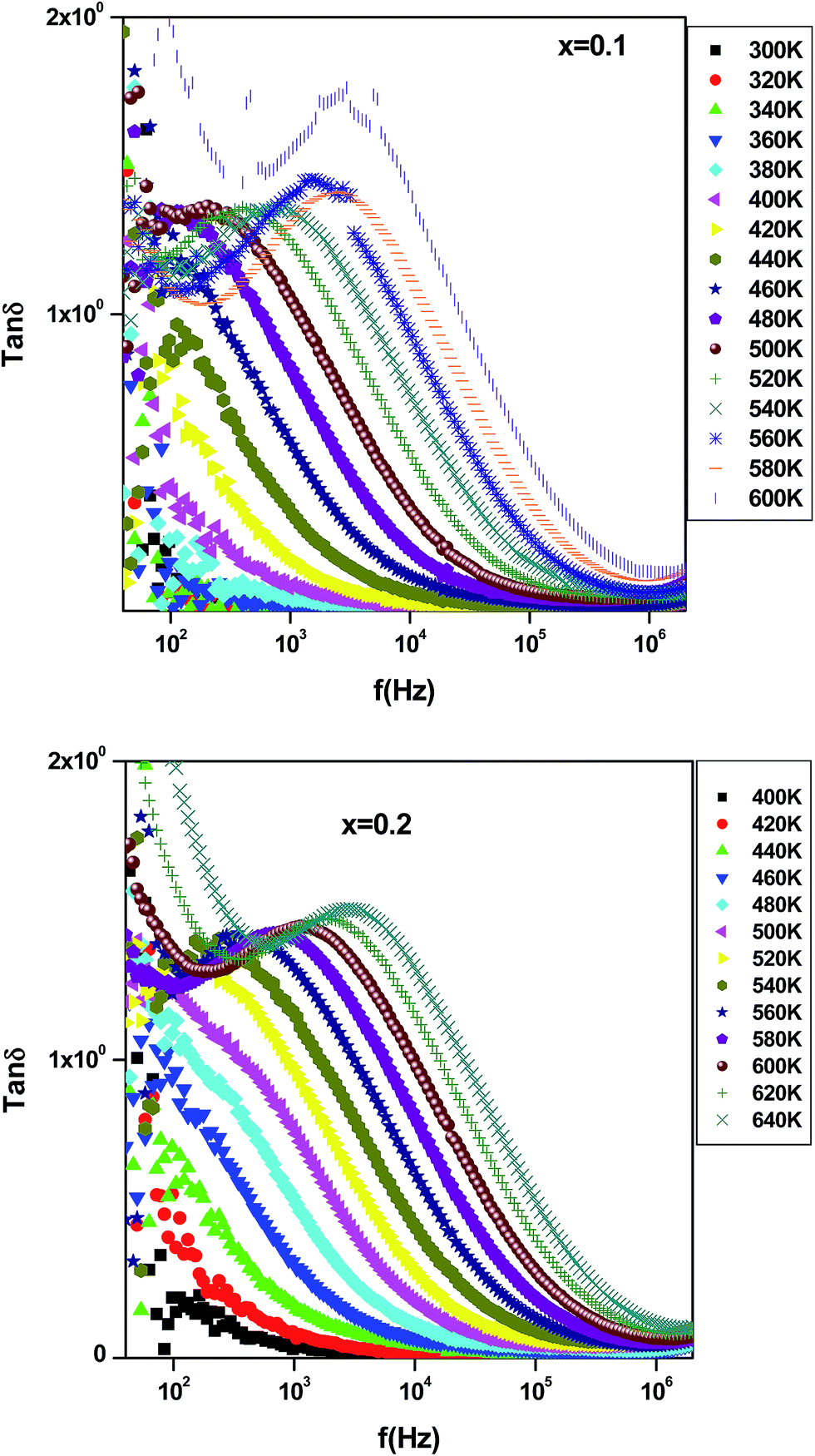
The increase of dielectric constant ε′ at low frequencies is associated to the heterogeneous conduction in the grain and grain boundary. The grain boundary region is characterized by a much higher resistivity. As shown in Fig. 10, the dielectric constant decreases with increasing Er content. In fact, this is attributed to the reduction in the A-site bismuth concentration and the reduction of oxygen vacancy concentration because the increasing of the substitution of Bi3+ by stable Er3+.41 The variation of tanδ as function of frequency and temperature is shown in Fig. 11. It is obvious that the dielectric loss increases with increasing temperature for all investigated samples. The tanδ plot shows a relaxation peak. The latter shifts toward high frequency side as temperature increases confirming the presence of dielectric relaxation in the material.42 Such relaxation can be explained by Maxwell–Wagner polarization.39,40 The observed behavior indicates that the investigated samples exhibit a characteristic of relaxor dielectric.
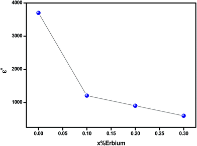 |
| | Fig. 10 Dielectric constant (ε′) of Bi4−xErxTi3O12 ceramics for different erbium content (at 520 K for 1 kHz). | |
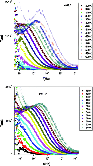 |
| | Fig. 11 Plot of (tanδ) versus frequency of Bi4−xErxTi3O12 at different temperatures. | |
4. Conclusion
We have investigated the structural, optical and electrical properties of polycrystalline Bi4Ti3O12 where the bismuth was substituted by erbium. The X-ray diffraction analysis revealed that all samples exhibit orthorhombic Fmmm structure. The feature peak of erbium is observed in absorbance spectra and their intensities increase with erbium content. DC-conductivity measurements indicate that the materials exhibit a semiconductor behavior in the whole explored temperature range. A significant decrease in σdc is observed when introducing Er content. For undoped sample, a saturation region appeared at a specific temperature (Tsat = 480 K) in σDC (T) curves. For the Er doped compounds, Tsat go beyond 600 K. It is found that conduction process is thermally activated and the values of the deduced activation energy suggest the possibility of electrical conduction due to the mobility of oxide ions or oxide ion vacancies at higher temperature. Conduction mechanism is well described by the jump relaxation model and conduction through grain boundaries. The frequency dependence of conductance followed the Jonscher law. The increase of Er leads to the decrease of the dielectric dispersion ε′. The tanδ plot indicates the presence of dielectric relaxation in the materials.
Acknowledgements
The authors would like to thank Mr Mohammed Sghaier Ben Rguiga from ETAP Tunis for his help in SEM observation.
References
- Y. Chen, Z. Pen, Q. Wang and J. Zhu, J. Alloys Compd., 2014, 612, 120 CrossRef CAS.
- F. Rehman, J. B. Li, M. S. Cao, Y. J. Zhao, M. Rizwan and H. B. Jin, Ceram. Int., 2015, 41, 14652 CrossRef CAS.
- R. Bokolia, O. P. Thakur, V. K. Raic, S. K. Sharma and K. Sreenivas, Ceram. Int., 2016, 42, 5718 CrossRef CAS.
- H. Yan, H. Zhang, R. Ubic, M. J. Reece, J. Liu, Z. Shen and Z. Zhang, J. Adv. Mater., 2005, 17, 1261 CrossRef CAS.
- L. Bellaiche and D. Vanderbilt, Phys. Rev. Lett., 1999, 83, 1347 CrossRef CAS.
- B. H. Park, B. S. Kang, S. D. Bu, T. W. Noh, J. Lee and W. Jo, Nature, 1999, 401, 682 CrossRef CAS.
- J. J. Wang, L. J. Feng, X. L. Chao, K. Zhao and A. J. Yan, Curr. Appl. Phys., 2013, 13, 1713 CrossRef.
- Z. Chen, X. Jiang, C. Zhu and C. Shi, Appl. Catal., B, 2016, 199, 241 CrossRef CAS.
- J. F. Dorrian, R. E. Newnham and D. K. Smith, Ferroelectrics, 1971, 3, 17 CrossRef CAS.
- L. L. Wang, W. H. Maa, Y. F. Fang, Y. Zhang, M. K. Jia, R. P. Li and Y. P. Huang, Procedia Environ. Sci., 2013, 18, 547 CrossRef CAS.
- J. Konig, M. Spreitzer, B. Jancar, D. Suvorov, Z. Samardzija and A. Popovic, J. Eur. Ceram. Soc., 2009, 29, 1695 CrossRef.
- F. Auzel, Chem. Rev., 2004, 104, 139–173 CrossRef CAS PubMed.
- L. F. Johnson, J. E. Guesic, H. J. Guggenheim, T. Kushida, S. Singh and L. G. Uitert, Appl. Phys. Lett., 1969, 15, 48–50 CrossRef CAS.
- J. Capobianco, F. Vetrone and J. Boyer, J. Phys. Chem. B, 2002, 106, 1181–1187 CrossRef CAS.
- H. Higushi, M. Takahashi, Y. Kawamoto, K. Kadono, T. Oshtsuki, N. Peyghambarian and N. Kitamura, Appl. Phys., 1998, 83, 19–27 Search PubMed.
- S. Madeswaran, N. V. Giridharan and R. Jayavel, Mater. Chem. Phys., 2003, 80, 23 CrossRef CAS.
- P. Pookmanee, P. Uriwilast and S. Phanichpant, Ceram. Interfaces, 2004, 30(7), 1913 CrossRef CAS.
- W. L. Liu, H. R. Xia, H. Han and X. Q. Wang, J. Mater. Sci., 2005, 40, 1827 CrossRef CAS.
- P. H. Xiang, Y. Kinemuchi, T. Nagaoka and K. Watari, Mater. Lett., 2005, 59(28), 3590 CrossRef CAS.
- O. Subohi, G. S. Kumar, M. M. Malik and R. Kurchania, Phys. B, 2012, 407, 3813 CrossRef CAS.
- A. Selmi, R. M'nassri, W. Cheikhrouhou-Koubaa, N. Chniba Boudjada and A. Cheikhrouhou, J. Alloys Compd., 2015, 619, 627 CrossRef CAS.
- N. Khare, D. P. Singh, H. K. Gupta, P. K. Siwach and O. N. Srivastava, J. Phys. Chem. Solids, 2004, 65, 870 CrossRef.
- A. Selmi, R. M'nassri, W. Cheikhrouhou-Koubaa, N. Chniba Boudjada and A. Cheikhrouhou, Ceram. Int., 2015, 41, 7723 CrossRef CAS.
- H. M. Rietveld, A profile refinement method for nuclear and magnetic structures, Appl. Crystallogr., 1969, 2, 65 CrossRef CAS.
- T. Roisnel and J. Rodriguez-Carvajal, Computer Program FULLPROF, LLB-LCSIM, 2003 Search PubMed.
- T. Takahashi and H. Iwahara, Mater. Res. Bull., 1978, 13, 1447 CrossRef CAS.
- J. J. Wang, L. J. Feng, X. L. Chao, K. Zhao and A. J. Yan, Curr. Appl. Phys., 2013, 13, 1713–1717 CrossRef.
- G. Parida and J. Beran, Ceram. Int., 2014, 40, 3139 CrossRef CAS.
- M. Zannen, H. Khemakhem, A. Kabadou and M. Es-Souni, J. Alloys Compd., 2013, 555, 56 CrossRef CAS.
- T. Badapanda, S. Sarangi, S. Parida, B. Behera, B. Ojha and S. Anwar, J. Mater. Sci.: Mater. Electron., 2015, 26, 3069 CrossRef CAS.
- K. Funke, Prog. Solid State Chem., 1993, 22, 111 CrossRef CAS.
- S. R. Elliot, Adv. Phys., 1987, 36, 135 CrossRef.
- A. K. Jonscher, Nature, 1977, 267, 673 CrossRef CAS.
- W. Chen, W. Zhu, O. K. Tan and X. F. Chen, J. Appl. Phys., 2010, 108, 034101 CrossRef.
- A. Pelaiz-Barranco, M. P. Gutierrez-Amador, A. Huanosta and R. Valenzuela, Appl. Phys. Lett., 1998, 73, 2039 CrossRef CAS.
- J. S. Kim, I. W. Kim, C. W. Ahn, T. K. Song, S. S. Kim, S. X. Chi, J. S. Bae and J. H. Jeong, Jpn. J. Appl. Phys., 2002, 41, 6785 CrossRef CAS.
- N. K. Singh, A. Panigrahi and R. N. P. Chaudhary, Mater. Lett., 2001, 50, 1 CrossRef CAS.
- T. Kar and R. N. P. Chaudhary, Mater. Sci. Eng., B, 2002, 90, 224 CrossRef.
- J. Maxwell, Electricity and Magnetics, V 1, S 328, Oxford University Press, London, 1873 Search PubMed.
- K. Wagner, Ann. Phys., 1913, 40, 817 CrossRef.
- R. Bokolia, O. P. Thakur, V. Rai, S. K. Sharma and K. Sreenivas, Ceram. Int., 2015, 41, 6055 CrossRef CAS.
- V. Hornebecq, C. Elissalde, V. Porokhonskyy, V. Bovtun, J. Petzelt, I. Gregora, M. Maglione and J. Ravez, J. Phys. Chem. Solids, 2003, 64, 471 CrossRef CAS.
|
| This journal is © The Royal Society of Chemistry 2017 |
Click here to see how this site uses Cookies. View our privacy policy here. 
 Open Access Article
 This Open Access Article is licensed under a
  *b and
K. Khirounia
*b and
K. Khirounia