
 Open Access Article
 This Open Access Article is licensed under a
 Creative Commons Attribution 3.0 Unported Licence
Design of boron vacancy enhanced spin filtering graphene/BN zigzag nanoribbon heterojunctions
Xiaohui Jiang ab,
Dongqing Zouc,
Bin Cuic,
Changfeng Fangb,
Wen Liub,
Xiangmu Kong*a and
Desheng Liu*bc
ab,
Dongqing Zouc,
Bin Cuic,
Changfeng Fangb,
Wen Liub,
Xiangmu Kong*a and
Desheng Liu*bc
aCollage of Physics and Engineering, Qufu Normal University, Qufu 273165, China. E-mail: kongxm@mail.qfnu.edu.cn
bDepartment of Physics, Jining University, Qufu 273155, People's Republic of China. E-mail: liuds@sdu.edu.cn
cSchool of Physics, State Key Laboratory of Crystal Materials, Shandong University, Jinan 250100, People's Republic of China
First published on 23rd January 2017
Abstract
The spin-polarized electronic transport properties of zigzag graphene nanoribbons (ZGNRs) and boron nitride nanoribbons (ZBNNRs) heterojunctions with a boron vacancy are investigated by using non-equilibrium Green's function and density functional theory, especially under an external electric field. The model we used in this paper is chosen from the last essay we researched, the I–V curves in the ferromagnetic states for (ZBNNR)5–(ZGNR)3–Bv devices are investigated, and the results show that with an external electric field, the heterojunctions are promising multifunctional devices in molecular spintronics due to their nearly perfect spin-filter effect, high rectification ratio and spin negative differential resistance properties at low biases. Mechanisms for such phenomena are proposed and these findings suggest a new opportunity for developing molecular spintronic devices.
Introduction
Graphene, a versatile material for its outstanding electronic properties, has proved useful in many devices applications.1–4 Recently, spin injection into graphene, low intrinsic spin orbital interaction, the observation of long spin lifetimes and lengths all suggests that graphene could play a good role in “spintronic” devices.5–7 Particularly, the ZGNRs are one of these systems and intensely studied due to the presence of magnetic states at their edges, and these states can be either antiparallel or parallel to each other (antiferromagnetic state AFM and ferromagnetic state FM), both the AFM and FM configurations' total energy are lower than the non-magnetic states', indicating that spin polarization is a stabilisation mechanism.8 However, for a ZGNR, the zero band gap limits its applications in electronics. In recent years, a number of theoretical and experimental feasible approaches are researched to open the band gap.9–13 Different isolated atomic crystals are assembled into designing heterostructures layer by layer via van del waals force between some 2D materials to open the energy gap, and these new materials show novel properties and phenomena.14–18 Recently, in-plane lateral heterostructures between graphene and hexagonal boron nitride (hBN) have been fabricated by controlling sizes and shapes to open the band gap.19,20 A monolayer of hBN is an insulator with a wide band gap of 5.9 eV whereas graphene is gapless semimetal. Both of them may coexist within a continuous atomically thin film, which might be experimentally accessible by many well-developed techniques in graphene.21,22 This kind of two-dimensional heterostructure could provide great opportunities towards the thin integrated circuit, and with properly designing the interface between graphene/hBN, the band gap and spin electronic property could be precisely engineered.As a promising candidate for applications in spintronics, recently, tremendous efforts have been devoted to manipulate the spin configuration. Son23 et al. have shown that with the applied of an electric field, the system was driven into a half-metallic state that one spin exhibits a metallic behavior, while the opposite spin experiences an increase in the energy gap. Simultaneously, chemical decorations of the ribbon edges can also enhance the effect and achieve effective robust spin filtering devices.24,25 Some other researchers have also suggested some other methods to get various spin-dependent properties, such as introducing quantum dots with the zigzag edges,26 functionalizing edges of GNRs27 and boron nitrogen doped for designated carbon atoms.28,29
In this work, we propose a series of ZBNNR/ZGNR heterojunction with a 100% SFE which can be tuned by the electric field and a boron vacancy (Bv) design. (ZBNNR)5–(ZGNR)3–Bv device has been researched in my last essay.30 From that paper, we know the magnitude current of (ZBNNR)5–(ZGNR)3–Bv device is very small, and there is no NDR phenomenon occurred. In this paper, we do further improvement of this model. The device of (ZBNNR)5–(ZGNR)3–Bv has semi-conducting electronic properties, and the semiconducting heterojunctions are well suited for a nano-electronic device application, because their electrical resistance can be easily controlled by the gate voltage. On the other hand, the metallic nano-materials have electrical resistance which is not sensitive to the gate voltage and this insensitivity has discouraged device applications, and led to designing the (ZBNNR)5–(ZGNR)3–Bv junctions.
Models and computational methods
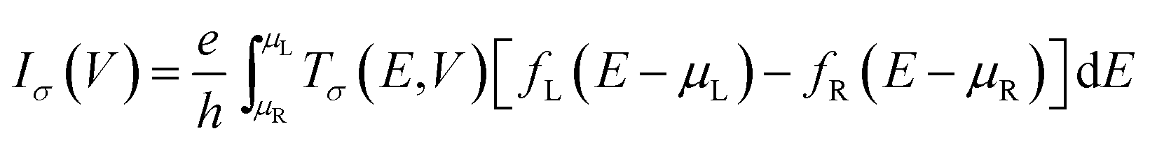
The models of (ZBNNR)5–(ZGNR)3–Bv heterojunctions are shown in Fig. 1. The heterojunction surface vectors are parallel with the x-axis and y-axis, respectively, and its transport direction is set along the z-axis. The two-probe device is divided into three parts, namely, the left electrode, the right electrode and the channel region. The left and right electrodes are made of ZGNRs, and the channel region is constructed by the (ZBNNR)5–(ZGNR)3 heterojunctions with a boron vacancy. Simultaneously, three-terminal FETs are constructed by adding a gate electrode under the channel region of the two-probe devices and the dielectric layer is used to insulate the channel from the gate. The quantum electronic transport properties of (ZBNNR)5–(ZGNR)3–Bv heterojunctions are calculated by applying the non-equilibrium Green's function (NEGF) combined with the density functional theory (DFT) by the software package Atomistix ToolKit (ATK). The electronic structures of left and right electrodes are obtained with periodic boundary conditions in all directions. Double-zeta polarized basis sets (DZP) are used as the local atomic numerical orbitals and the spin generalized gradient approximations (SGGA) are used as the exchange correlation function. The convergence criteria of energy and force of all atoms in the channel region are set to be 1 × 10⁻⁵ eV and 0.05 eV Å−1, respectively. A 1 × 1 × 100 Monkhorst sampling in the Brillouin zone is utilized and cut-off energy for the electrostatic potentials is 75 hartree. The electronic temperature is set at 300 K. The spin-dependent current under the bias voltage through the channel region is calculated by Landauer–Büttiker formula:31where Tσ(E,V) is the bias and spin dependent transmission coefficient, fL/R(E) = 1/{1 + exp[(E − μL/R)/KBT]} is the Fermi–Dirac distribution function of the right and left electrode. σ is the spin index (↑,↓), respectively.
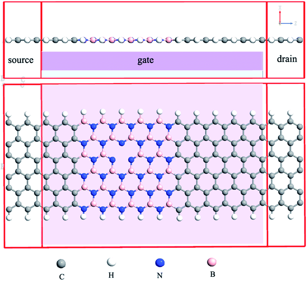 | ||
| Fig. 1 Schematics of (ZBNNR)5–(ZGNR)3–Bv three-terminal FET. The gate electrode is denoted by the gray box with a thickness of 0.5 Å and the purple box represents the dielectric layer with a dielectric constant of 4. | ||
Results and discussion
In order to understand the changes in the spin-dependent electronic transport properties by applying an external electric field, the zero bias transmission spectra of (ZBNNR)5–(ZGNR)3–Bv FET devices are plotted in Fig. 2 under several gate voltages of −4 V, −2 V, 0 V, 2 V and 4 V, respectively, and the transmission coefficients near Ef vary significantly. From Fig. 2(a), while Vg = 0 V, we can see distinct spin polarized transmission peaks appear below the Ef, and with the increase of Vgs (Vg = −2 V, −4 V), the transmission spectra move to a higher energy, which means negative gate voltages can raise the orbital energy. Simultaneously, the migration of spin down spectra is larger than spin up spectra, which result in a giant spin splitting of the transmission spectra at Ef, indicating that this device can be used as a spin filter. Conversely, in Fig. 2(d) and (e), with the increase of the positive gate voltages (Vg = 2 V, 4 V), large energy gaps are observed and the transmission spectra shift to the lower energy, and there are no peaks around the Ef, which means the positive gate voltages have great influence on the electronic transport properties, but the spin polarized phenomena decreased.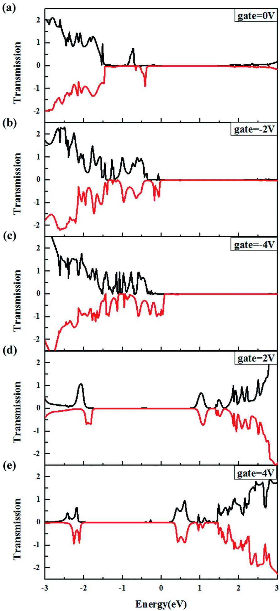 | ||
| Fig. 2 (a)–(e) shows the spin-dependent transmission spectra of (ZBNNR)5–(ZGNR)3–Bv FET device at Vg = 0 V, −2 V, −4 V, 2 V, 4 V with Vb = 0 V, respectively. | ||
Fig. 3(a)–(e) shows the projected density of states of (ZBNNR)5–(ZGNR)3–Bv FET device on the carbon atoms (PDOS–C), boron and nitrogen atoms (PDOS–BN) and total density of states (TDOS) under Vg = 0 V, −2 V, −4 V, 2 V, and 4 V with bias = 0 V, respectively. Compared with Fig. 3(a) and (c), we can see different phenomena at Ef. While Vg = 0 V, there are no peaks at Ef for both spin up and spin down channels. As the gate voltage increases to −4 V, a large peak appears at Ef for the spin down channel, and the PDOS–C and PDOS–BN indicate that the TDOS at Ef mainly derives from the PDOS–BN. The magnitude of PDOS–C nearly to zero, which means the ZBNNRs to contribute to the spin dependent transport properties. It is in accordance with the transmission eigenstates in Fig. 3(f). While Vg = −4 V, the transmission eigenstates in the spin up channel are almost localized on the left side, however, the transmission eigenstates delocalized through the whole scattering region in the spin down channel, and the eigenstates are almost localized on the nitrogen and boron atoms. We also can see the eigenstates on the nitrogen and boron atoms around the vacancy are delocalized, and work as a scattering center for the electrons propagating along the nanoribbons, which prove the vacancy does great contributions to the spin dependent electronic transport properties. While applying the positive gate voltages, from Fig. 3(d) and (e), we can see the peaks of TDOS mainly derive from the PDOS–C, which means carbon atoms play an important role in the transport channels. The corresponding transmission eigenstates (Fig. 3(f)) show both in spin up and spin down channels, the eigenstates are predominantly localized on the left carbon atoms, which leads to a relatively small current, so in our following paper we only discuss the effect of the negative gate voltages.
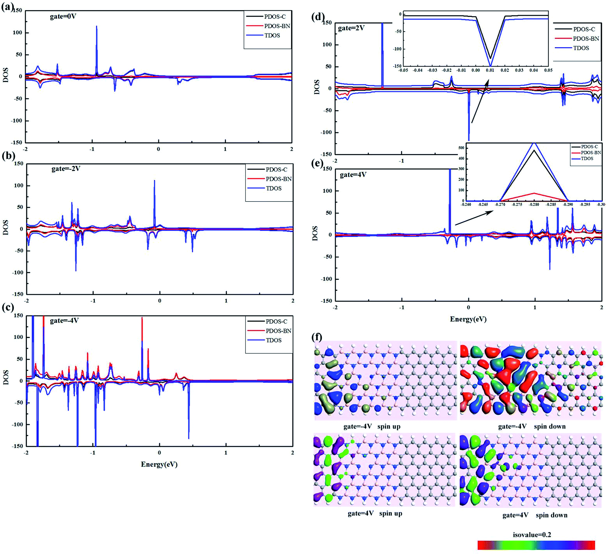 | ||
| Fig. 3 (a)–(e) shows the spin-dependent total and projected density of states of (ZBNNR)5–(ZGNR)3–Bv FET device at Vg = 0 V, −2 V, −4 V, 2 V, 4 V with Vb = 0 V, respectively; (f) shows the spin up and spin down transmission eigenstates at Ef with Vg = −4 V and 4 V, respectively. | ||
Previous studies have shown that the effects of spin polarization of the ZGNR edges can be different under external electric field and the current polarization can also be found.23 Here, we also examine the effects of an external electric field on (ZBNNR)5–(ZGNR)3–Bv device. In Fig. 4(a), we show the spin-dependent currents under zero and two negative gate voltages of Vg = 0 V, −2 V and −4 V, respectively. From the inset graph of Fig. 4(a), at Vg = 0 V, both the spin up and spin down currents are small and display semiconductor behaviors, therefore these heterojunctions can be manipulated by the gate voltages. With the increase of negative gate voltages, the currents of both spin channels rise at the same time, especially at Vg = −2 V and −4 V, and spin negative differential resistance (SNDR) phenomena can also be observed except for the spin up channel of Vg = −2 V. As the negative gate voltage increases to −4 V, both spin channels have obvious NDR properties but start at different biases, i.e., 0.8 V for the spin up channel and −0.9 V, −0.2 V, 0.5 V, 0.8 V for the spin down channel. The magnitude of the current in the spin down channel is larger than that in the spin up channel in the whole bias range with the increase of the negative gate voltages, which is different from Vg = 0 V. The negative gate voltages suppress the transport of the spin up channel and promote the transport of the spin down channel, thus leading to sharp contrast forms the mechanism of electrical-field-tuned spin filter effects for ZGNRs.
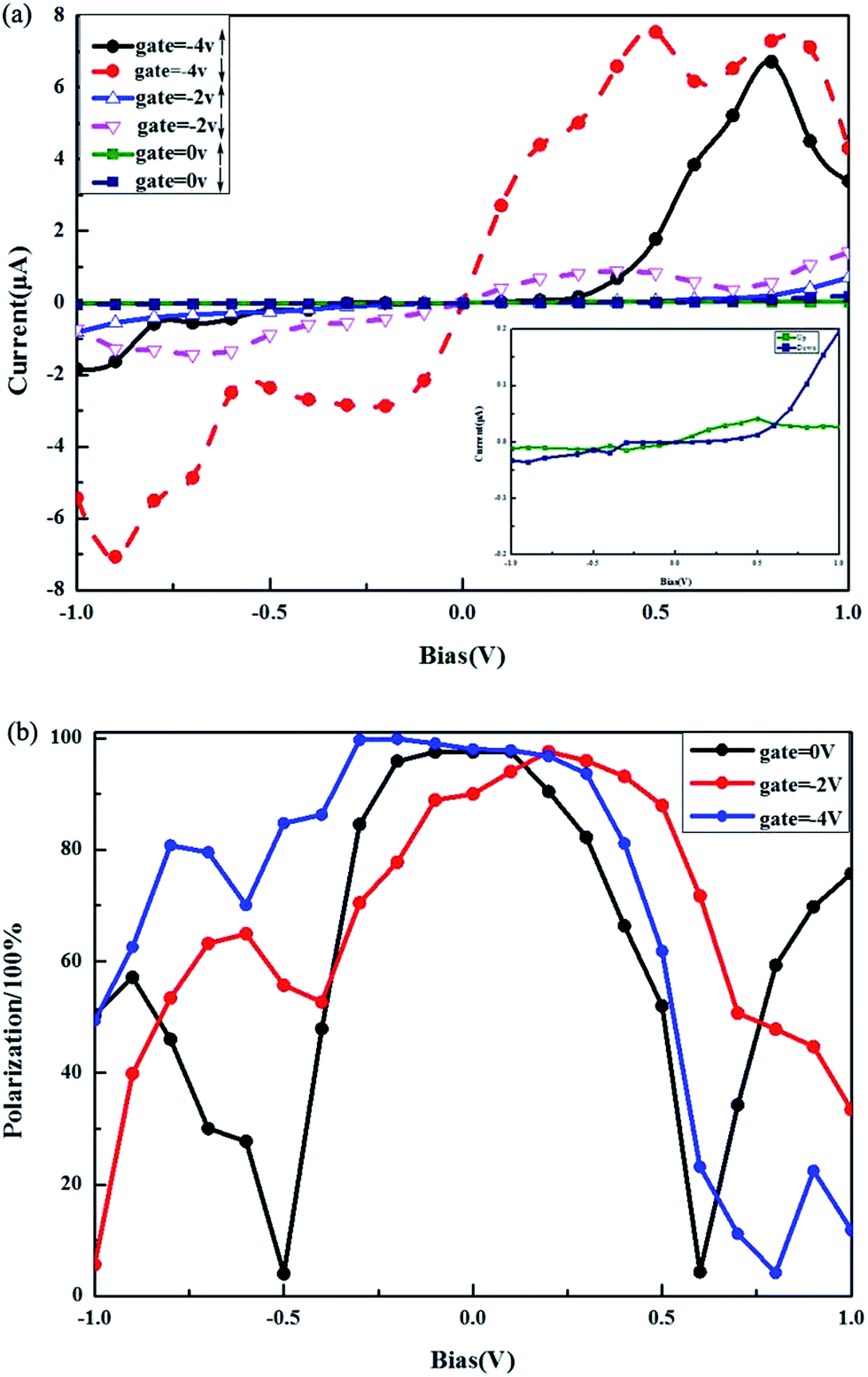 | ||
| Fig. 4 (a) shows the calculated spin-dependent current–voltage characteristics for the (ZBNNR)5–(ZGNR)3–Bv device under different Vgs (Vg = −4 V, −2 V, 0 V), respectively. Inset: the amplified I–V curve of (ZBNNR)5–(ZGNR)3–Bv device under Vg = 0 V. (b) shows the spin-filter efficiency (SFE) as a function of the electric field intensity and bias for (ZBNNR)5–(ZGNR)3–Bv device, Vg = −4 V, −2 V, 0 V, respectively. | ||
Fig. 4(b) shows the spin filter effects (SFE) under different negative gate voltages. We define the SFE at finite bias as:
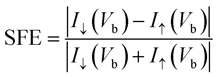
where T↓(Ef) and T↑(Ef) represent the transmission coefficient of the spin down and spin up channel at the Fermi level, respectively. Obviously, as can be seen from Fig. 4(b), SFE are extremely sensitive to the negative gate voltages and bias voltages, and the capability of spin-filter at Vg = −2 V and −4 V is larger than that at Vg = 0 V. Nearly 100% SFE can be observed in the bias range of −0.3 V to 0.2 V. Therefore, we are able to design a spin filter based on (ZBNNR)5–(ZGNR)3 heterojunctions with a boron vacancy under negative gate voltages.
In order to understand the origin of SFE behavior, the electronic density of states (DOS) and molecular energy levels in the scattering region are plotted on the transmission spectra in Fig. 5(a) and (b), at Vg = −4 V, with Vb = −0.3 V, 0.6 V, respectively. Simultaneously, the dashed blue lines represent the position of the first four frontier molecular orbitals are marked with HOMO−1, HOMO (the highest occupied molecular orbital), LUMO (the lowest unoccupied molecular orbital) and LUMO+1 of the spin up and spin down channels. It can be found that one molecular orbital appears in the bias window (marked by the two purple lines) at −0.3 V for the spin up channel, whereas no transmission peak appears. Obviously the transmission and the DOS spectra are strongly correlated with each other in Fig. 5(a), while the transmission coefficients are determined by the delocalization of the frontier molecular orbitals and the molecular projected self-consistent Hamiltonian (MPSH) for each frontier orbital is drawn in Fig. 5(c). For the spin up channel, the MPSHs of HOMO, LUMO and LUMO+1 are all localized on one end of the device, which means an electron is hard to tunnel through the junction and the transport paths are closed, thus the transmission coefficients are extremely small. Oppositely, for the spin down channel, there are three molecular orbitals and a big transmission peak appearing in the bias window. All the HOMO−1, HOMO, LUMO and LUMO+1 are delocalized, which means the electronic transport paths for the spin down channel are open, and large electronic current can be obtained, which results in the SFE phenomena occurred. In Fig. 5(b), as the bias increases to 0.6 V, for the spin up channel, it is clear that a wide big peak moves into the bias window, and HOMO−1 orbital also moves into the bias window. The HOMO−1 and HOMO orbitals are delocalized, then the electronic transmission capability for the spin up channel increases to a certain extent. Moreover, for the spin down channel, HOMO−1 orbital moves into the bias window, and there are four orbitals in the bias window, thus the electronic transmission capability for the spin down channel is also larger than the spin up channel. Compared with Fig. 5(a), for the spin up is improved, resulting in a reduced SFE, as shown in Fig. 4(b).
 | ||
| Fig. 5 (a)–(b) shows the spin-dependent transmission spectra and the electronic density of states of (ZBNNR)5–(ZGNR)3–Bv device at Vg = −4 V with Vb = −0.3 V, 0.6 V, respectively. The vertical solid purple lines stand for bias window, and the dashed blue lines represent the spin-polarized Frontier molecular orbitals. (c)–(d) shows the MPSH of the corresponding spin-dependent HOMO−1, HOMO, LUMO and LUMO+1 under bias of −0.3 V and 0.6 V, respectively. | ||
Another attractive result is the NDR behaviors. Especially at Vg = −4 V, a notable NDR phenomenon can be observed at both spin up and spin down channels. In Fig. 6, we show the transmission spectra and electronic density of states for spin down channel at Vb = 0.1 V, 0.5 V and 1.0 V under Vg = −4 V and Vg = 0.0 V, respectively. Compared with the Fig. 6(d)–6(f), we can see that, at Vg = 0.0 V, the transmission spectra are almost the same in the bias window and no peaks appeared. However, with the increase of the negative gate voltages, the transmission peaks move into the bias window, and NDR phenomenon occurred. In Fig. 6(a), we can see the bias window is narrow, and contains a little transmission peaks. As Vb increases to 0.5 V, the bias window expands and more transmission peaks move into it, resulting in the current increased. Due to increasing the Vb further, the bias window becomes larger accordingly, however, the transmission peaks in the bias window become localized into two narrow peaks, and the magnitude of DOS peaks in the bias window decreased largely. For this reason, at Vb = 1.0 V, although there are two narrow localized transmission peaks in the bias window, the current decreases and NDR appears. From Fig. 6(d) and (e), we can see a large DOS peak above the Fermi level, however, the transmission coefficients are almost zero. To illuminate this phenomena, local density of states (LDOS) at 0.49 eV, 0.59 eV and 0.69 eV are calculated and given in the insets of Fig. 6. From the image of the LDOS, we can see the electron states at the DOS peaks localized at the boundaries, and the transport paths are closed, thus the transmission coefficients are almost zero. For the above illustration, it is concluded that the applied gate electrodes can change the coupling between the molecular orbitals and the electrodes, which resulting in an obvious NDR behavior.
 | ||
| Fig. 6 Transmission spectra and electronic density of states of (ZBNNR)5–(ZGNR)3–Bv device for spin down channel. (a)–(c) represents Vb = 0.1 V, 0.5 V and 1.0 V at Vg = −4 V, respectively. (d)–(f) represents Vb = 0.1 V, 0.5 V and 1.0 V at Vg = 0.0 V, respectively. Their LDOS are shown in the corresponding insets with an isovalue of 0.03. The region between the vertical purple lines is the bias window. | ||
In order to understand the RR behavior, we show the electronic transport properties of (ZBNNR)5–(ZGNR)3–Bv device for spin up channel under the applied gate Vg = −4 V in Fig. 7. The rectification ratio (RR) is defined as
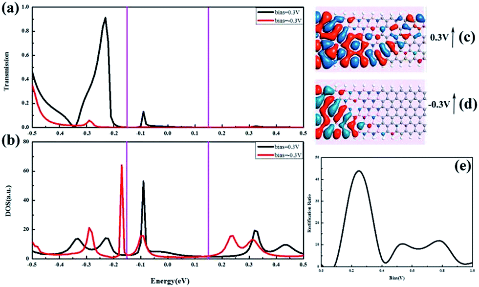 | ||
| Fig. 7 (a) Transmission spectrum, (b) projected density of states (black line for 0.3 V, red line for −0.3 V) of (ZBNNR)5–(ZGNR)3–Bv devices for spin up channel under the applied gate Vg = −4 V. (c) and (d) represents the corresponding transmission eigenstates at the Fermi level. (e) RR for the spin up channel, and the solid purple lines indicate the bias window. | ||
The ratio of the current under the positive and negative biases with the same voltage magnitude. As shown in Fig. 7(e), at bias 0.3 V, RR = 44 for the spin up channel. Fig. 7(a) shows the transmission spectrum at bias 0.3 V and −0.3 V. In the bias window, one peak appears at bias 0.3 V and no peaks appear at bias −0.3 V, indicating the conductance at 0.3 V is larger than that at −0.3 V, which is in accordance with the DOS in Fig. 7(b). The corresponding transmission eigenstates at Ef in the spin up channel at bias 0.3 V are delocalized through the whole scattering region, however, at bias −0.3 V, the transmission eigenstates at Ef are almost localized on the left side, as shown in Fig. 7(c) and (d). As a result, we can see that the RR at bias 0.3 V is very high.
Conclusions
In summary, based on first-principle quantum transport calculations, we have shown the spin dependent electronic transport properties of (ZBNNR)5–(ZGNR)3–Bv device under external electric field. Compared to the results of the (ZBNNR)5–(ZGNR)3–Bv device without electric field, a nearly perfect SFE, high RR and SNDR behaviors can be obtained under the electric field in the ferromagnetic states. The mechanism on the phenomena is illustrated by the spin population analysis in details. The spin filter effects can be easily tuned and improved by the applied gate voltages, especially for the negative gate voltages. The reason is the negative gate voltages can tune the spin down channel obviously, and have little influence for the spin up channel. With the high RR and SNDR behaviors, a logic gates are potential to be designed and these findings suggest new possibilities for developing nanometer spintronic devices.Acknowledgements
This work was supported by the National Natural Science Foundation of China (Grant No. 11374183, 11574118, 11275112 and 11404141).References
- K. S. Novoselov, A. K. Geim, S. V. Morozov, D. Jiang, Y. Zhang, S. V. Dubonos, I. V. Grigorieva and A. A Firsov, Science, 2004, 306, 666 CrossRef CAS PubMed.
- G. Eda, G. Fanchini and M. Chhowalla, Nat. Nanotechnol., 2008, 3, 270 CrossRef CAS PubMed.
- Y. B. Tang, C. S. Lee, Z. H. Chen, G. D. Yuan, Z. H. Kang, L. B. Luo, H. S. Song, Y. Liu, Z. B. He, W. J. Zhang, L. Bello and S. T. Lee, Nano Lett., 2009, 9, 1374 CrossRef CAS PubMed.
- X. Yang, G. Liu, A. A. Balandin and K. Mohanram, ACS Nano, 2010, 4, 5532 CrossRef CAS PubMed.
- M. Ohishi, M. Shiraishi, R. Nouchi, T. Nozaki, T. Shinjo and Y. Suzuki, Jpn. J. Appl. Phys., 2007, 46, 25 CrossRef.
- B. Trauzettel, D. V. Bulaev, D. Loss and G. Burkard, Nat. Phys., 2007, 3, 192 CrossRef CAS.
- D. Huertas-Hernando, F. Guinea and A. Brataas, Phys. Rev. B: Condens. Matter, 2006, 74, 2952 CrossRef.
- L. Pisani, J. A. Chan, B. Montanari and N. M. Harrison, Phys. Rev. B: Condens. Matter Mater. Phys., 2006, 75, 794 Search PubMed.
- Y. L. Lee, S. Kim, C. Park, J. Ihm and Y. W. Son, ACS Nano, 2010, 4, 1345 CrossRef CAS PubMed.
- Y. Zhang, T. T. Tang, C. Girit, Z. Hao, M. C. Martin, A. Zettl, M. F. Crommie, Y. R. Shen and F. Wang, Nature, 2009, 459, 820 CrossRef CAS PubMed.
- J. W. Bai, X. Zhong, S. Jiang, Y. Huang and X. F. Duan, Nat. Nanotechnol., 2010, 5, 190 CrossRef CAS PubMed.
- C. R. Dean, A. F. Young, I. Meric, C. Lee, L. Wang, S. Sorgenfrei, K. Watanabe, T. Taniguchi, P. Kim, K. L. Shepard and J. Hone, Nat. Nanotechnol., 2010, 5, 722 CrossRef CAS PubMed.
- L. Britnell, R. V. Gorbachev, R. Jalil, B. D. Belle, F. Schedin, A. Mishchenko, T. Georgiou, M. I. Katsnelson, L. Eaves, S. V. Morozov, N. M. Peres and J. Leist, Science, 2012, 335, 947 CrossRef CAS PubMed.
- A. K. Geim and I. V. Grigorieva, Nature, 2013, 499, 419 CrossRef CAS PubMed.
- B. Hunt, J. D. Sanchez-Yamagishi, A. F. Young, M. Yankowitz, B. J. Leroy, K. Watanabe, T. Taniguchi, P. Moon, M. Koshino, P. Jarillo-Herrero and R. C. Ashoori, Science, 2013, 340, 1427 CrossRef CAS PubMed.
- K. S. Novoselov, V. I. Fal'Ko, L. Colombo, P. R. Gellert, M. G. Schwab and K. Kim, Nature, 2012, 490, 192 CrossRef CAS PubMed.
- N. Kharche and S. K. Nayak, Nano Lett., 2011, 11, 5274 CrossRef CAS PubMed.
- L. A. Ponomarenko, A. K. Geim, A. A. Zhukov, R. Jalil, S. V. Morozov, K. S. Novoselov, I. V. Grigorieva, E. H. Hill, V. V. Cheianov, V. I. Fal’ko, K. Watanabe, T. Taniguchi and R. V. Gorbachev, Nat. Phys., 2011, 7, 958 CrossRef CAS.
- M. P. Levendorf, C. J. Kim, L. Brown, P. Y. Huang, R. W. Havener, D. A. Muller and J. Park, Nature, 2012, 488, 627 CrossRef CAS PubMed.
- Z. Liu, L. Ma, G. Shi, W. Zhou, Y. Gong, S. Lei, X. Yang, J. Zhang, K. P. Hackenberg, A. Babakhani, J. C. Idrobo, R. Vajtai, J. Lou and P. M. Ajayan, Nat. Nanotechnol., 2013, 8, 119 CrossRef CAS PubMed.
- V. O. Özçelik and S. Ciraci, Physics, 2013, 117, 15327 Search PubMed.
- A. G. Garcia, M. Neumann, F. Amet, J. R. Williams, K. Watanabe, T. Taniguchi and D. Goldhaber-Gordon, Nano Lett., 2012, 12, 4449 CrossRef CAS PubMed.
- Y. W. Son, M. L. Cohen and S. G. Louie, Nature, 2007, 444, 347 CrossRef PubMed.
- O. Hod, V. Barone, J. E. Peralta and G. E. Scuseria, Nano Lett., 2007, 7, 2295 CrossRef CAS PubMed.
- D. Gunlycke, J. Li, J. W. Mintmire and C. T. White, Appl. Phys. Lett., 2007, 91, 112108 CrossRef.
- O. Hod, V. Barone and G. E. Scuseria, Phys. Rev. B: Condens. Matter Mater. Phys., 2008, 77, 035411 CrossRef.
- F. Cervantes-Sodi, G. Csanyi, S. Piscanec and A. C. Ferrari, Phys. Rev. B: Condens. Matter, 2008, 77, 165427 CrossRef.
- E. J. Kan, X. J. Wu, Z. Y. Li, X. C. Zeng, J. L. Yang and J. G. Hou, J. Chem. Phys., 2008, 129, 084712 CrossRef PubMed.
- F. Zheng, G. Zhou, Z. Liu, J. Wu, W. Duan, B. L. Gu and S. B. Zhang, Phys. Rev. B: Condens. Matter Mater. Phys., 2008, 78, 205415 CrossRef.
- X. H. Jiang, C. F. Fang, D. Q. Zou, W. K. Zhao, W. Liu, X. M. Kong and D. S. Liu, RSC Adv., 2016, 6, 56429 RSC.
- M. Büttiker, Y. Imry, R. Landauer and S. Pinhas, Phys. Rev. B: Condens. Matter Mater. Phys., 1985, 31, 6207 CrossRef.
| This journal is © The Royal Society of Chemistry 2017 |