
 Open Access Article
 This Open Access Article is licensed under a Creative Commons Attribution-Non Commercial 3.0 Unported Licence
High-yield and rapid synthesis of ultrathin silver nanowires for low-haze transparent conductors†
Yang Liu,
Yingying Chen,
Rui Shi,
Lijun Cao,
Zhan Wang,
Tao Sun,
Jianjian Lin,
Juqing Liu* and
Wei Huang *
*
Key Laboratory of Flexible Electronics (KLOFE), Institute of Advanced Materials (IAM), Jiangsu National Synergistic Innovation Center for Advanced Materials (SICAM), Nanjing Tech University (NanjingTech), 30 South Puzhu Road, Nanjing 211816, P. R. China. E-mail: iamjqliu@njtech.edu.cn; iamwhuang@njtech.edu.cn
First published on 17th January 2017
Abstract
Ultrathin silver nanowires (Ag NWs) have been rapidly synthesized by using NaBr and AgCl as conucleant, with a high yield of 90%. The average diameter and length of Ag NWs is 30 nm and 11 μm, respectively. The resulting conductor exhibits high ratio of DC conductivity to optical conductivity of 162, low sheet resistance of 12.2 Ω sq−1 at 83.3% and low haze of 0.96% at 95.7%.
Transparent conducting electrodes (TCEs) are essential components in various optoelectronic devices such as solar cells, organic light emitting diodes, liquid crystal displays, touch screens, and smart windows.1,2 Nowadays, the most common conductive material used in TCEs is indium tin oxide (ITO). However, poor mechanical flexibility, limited supply, high cost, and the vacuum forming process of the ITO layer have become an obstacle for its further development in conductors, together with limitations in future electronics.3 Several alternative materials have been developed to replace ITO, such as carbon nanotubes (CNTs),4–6 conductive polymers,5,6 graphene,4–7 metal nanowires,4,5,7 and hybrid electrodes.5,7 Among them, metal nanowire conductive materials, mainly silver nanowires (Ag NWs) and copper nanowires (Cu NWs), have been widely explored for their promising opto-electrical properties and outstanding mechanical flexibility. It is noted that Ag NWs exhibit excellent electrical conductivity, superior electrical, and thermal conductivities compared with other metals.1–3,8–15 Therefore, Ag NWs are widely considered to be the optimal material for fabricating flexible electronics.
To synthesize Ag NWs, numerous methods have been employed, such as template wetting and polyol.16,17 The polyol method has been recognized as one of the most promising processes to reliably prepare Ag NWs, with the advantage of facile and controllable synthesis, and large-scale manufacturing and low-cost potential,11,13–15 to obtain the high performance Ag NW conductors, tremendous efforts have been made to synthesis uniform Ag NWs with long length and thin diameter.10–15,18–24 For example, Bergin et al.26 reported the synthesis of Ag NWs by the polyol method, with a thin diameter of 42 nm. However, the nanowires were very short, with a length of 3 μm. More recently, Kim et al.12 successfully demonstrated the synthesis of high quality Ag NWs with an average length of 13.5 μm and diameter up to 62.5 nm. Thinner diameter Ag NW formation can be achieved when high pressure is applied in an autoclave reactor, instead of the typical synthesis under atmospheric pressure.25 Zhang, et al.37 reported a facile one-pot polyol method to synthesis Ag NWs by using KBr as a co-nucleant to NaCl with long reaction time. The aspect ratio is crucial for the opto-electric properties of Ag NWs. Lee et al.18 shows short (L = 10.2 μm) Ag NW films (T = 77.21%, Rs = 34 Ω sq−1), long (L = 95.1 μm) Ag NW films (T = 96%, Rs = 186 Ω sq−1). Preston et al.13 shows large diameters (D = 150 nm) Ag NW films (T = 75%, Rs = 135 Ω sq−1), small diameters (D = 60 nm) Ag NW films (T = 78%, Rs = 45 Ω sq−1). Therefore, high yield and rapid synthesis of ultrathin Ag NWs is necessary in commercial application of the emerging Ag NW conductors.
In this work, we report a modified polyol approach, using NaBr and AgCl as conucleant, for rapid synthesis of ultrathin, high quality, and monodispersed Ag NWs, with an average diameter of 30 nm and a mean length of 11 μm. Impressively, this efficiency approach is also associated with high yield of ultrathin Ag NW products, with a value up to 90%. The resulting ultrathin Ag NW conductors show excellent conductivity, optical transparency, and low haze in comparison with previous reports. All these advances are expected to enable more possibilities for use of Ag NWs in future emerging conductors.
In order to synthesize an ultrathin Ag NWs suspension in ethanol, 0.012 g NaBr (sodium bromide) was first added in 14 mL ethylene glycol (EG) containing 0.66 g polyvinylpyrrolidone (PVP, Mw = 1![[thin space (1/6-em)]](https://www.rsc.org/images/entities/char_2009.gif) 300000), and then the mixture was stirred at 200 rpm and thermally stabilized at 165 °C. Secondly, 0.05 g silver chloride (AgCl) in a 2 mL EG solution was added to the mixture.
300000), and then the mixture was stirred at 200 rpm and thermally stabilized at 165 °C. Secondly, 0.05 g silver chloride (AgCl) in a 2 mL EG solution was added to the mixture.
After three minutes, 4 mL of EG solution containing 0.22 g AgNO3 was injected with syringe using at a rate of 0.4 mL min−1, the reaction was left for 30 min to allow the nanowires to grow. Finally, the Ag NW product was collected via centrifugation, washed with ethanol; the resulting suspension was used for subsequent characterization and conductor fabrication.
Fig. 1 shows scanning electron microscopy (SEM) images and size distribution of the reaction product synthesized under different growth conditions. Reducing AgNO3 by using AgCl for the nucleation of silver seed resulting in synthesis of thin Ag NWs, and irregular silver nanoparticles (Ag NPs) were observed without addition of AgCl and NaBr, meaning reducing solvents plays a key role in achieving nanowire features. Moreover, ultrathin Ag NWs were synthesized by using NaBr and AgCl as conucleant. The thin Ag NWs exhibit a diameter of 49.5 ± 15.0 nm and length of 7.0 μm (the size distribution of Ag NWs were counted by a nano measurer), which is comparable to that by gram-scale polyol synthesis26 but are of significantly higher quality than those of previous methods.10,12,29 Compared to the thin Ag NWs, our ultrathin nanowires have a much smaller diameter and longer length, with the value of 30.4 ± 9.0 nm and 11.0 μm, respectively. This diameter thinning from 50 nm to 30 nm after the introduction of NaBr during the reduction process, indicates the role of NaBr being crucial in synthesizing ultrathin Ag NWs.
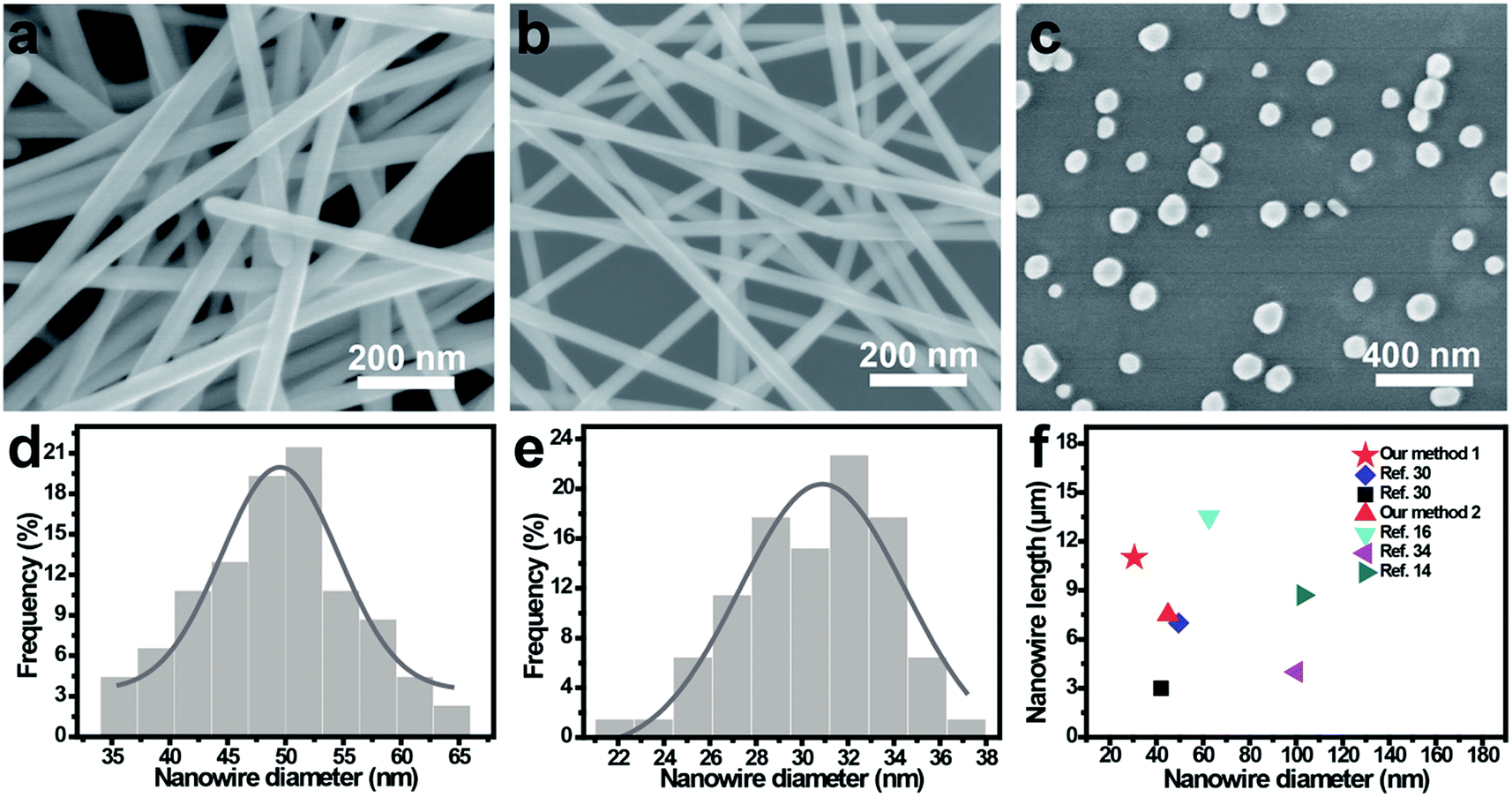 | ||
| Fig. 1 SEM images of the products (a) with addition of AgCl, (b) with addition of AgCl and NaBr, (c) without addition of AgCl and NaBr. Histogram show the diameter distribution of (d) thin Ag NWs and (e) ultrathin Ag NWs, which corresponding to product (a) and (b), respectively. (f) Diameter and length comparison of Ag NW products synthesized using polyol process method in the literature. | ||
To understand the growth mechanism and subsequent morphology, we propose that the diameter decrease in the present method could be attributed to the lower solubility product (Ksp) of AgBr compared to that of AgCl. Tang et al.27 reported that Ag NPs were actually produced from AgCl by heating an AgCl solution, and the concentration of silver nuclei plays a crucial role for formation and the size of silver seeds.15,28 It is well known that Ksp of AgCl is higher than that of AgBr, meaning that more Ag nuclei are generated during the reduction of silver ions by AgCl, resulting in high concentration of Ag nuclei, which trigger the formation of large-size silver seeds. By injecting AgNO3 slowly, the amount of free Ag+ ions in solution for AgCl system is higher than that for the AgCl and NaBr hybrid system, the kinetics of the reduction process of AgNO3 are slowed down due to the lower Ksp of AgBr, resulting in a lower concentration of Ag+ ions, which prefer to form ultrathin Ag NWs through small-size Ag seeds as initiation. Moreover, our method has a quicker reaction time overall than those previously reported4,11,14,15 at 30 min. Hence, this technique may be a very promising solution for the mass-production of low-cost Ag NWs.
Although well established in characterization technology, UV-visible spectroscopy has been used to investigate the morphological evolution of silver nanostructures due to the frequencies of surface plasmon resonances.30,31 Using this method, we obtained UV-visible absorption spectra of the final products under different growth conditions, as shown in Fig. 2 typical broad peak at 453–463 nm was observed for the products without AgCl and NaBr, indicating the formation of Ag NPs. However, a narrow peak at 376 nm with a distinct shoulder was found for thin Ag NWs, which is consistent with previous results.15,32 Impressively, the ultrathin Ag NWs exhibit a sharp peak at 373 nm with a slight shoulder, meaning the diameter decrease for Ag NWs is accompanied by a blue shift and narrow bandwidth of UV absorption spectra. In addition, the structure of ultrathin Ag NWs were studied by X-ray diffraction (XRD) shown in Fig. S1.† The nanowires exhibit four typical peaks, which corresponded to the diffraction of (111), (200), (220), (311) Ag planes, suggesting that the ultrathin Ag NWs are high quality and pure.14,34
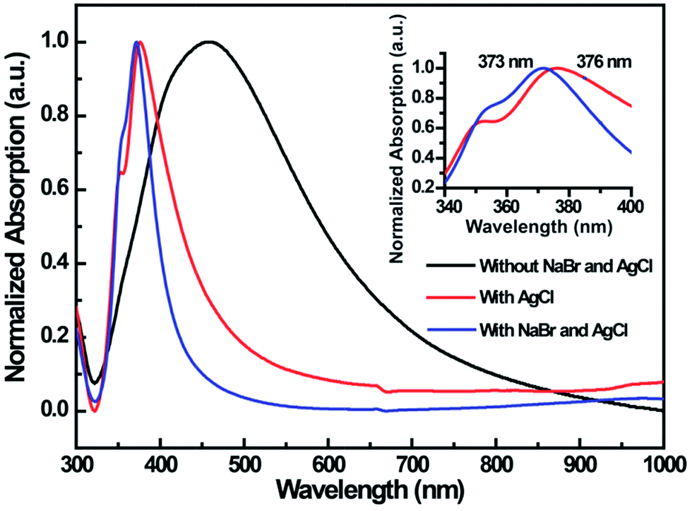 | ||
| Fig. 2 UV-visible absorption spectra of the final products under different growth conditions. The inset represents the corresponding selected peaks ranging from 340 nm to 400 nm. | ||
To further examine the effect of stirring speeds on the Ag NW synthesis, three different stirring speeds (0, 200, and 400 rpm) for the same reaction time and temperature were carried out. Fig. 3a–f and S3a–c† shows the SEM images and length distribution of the Ag NWs obtained in AgCl and NaBr mixture under different stirring speed. The results show that the average length of Ag NWs at is 9 μm at 0 rpm, 11 μm at 200 rpm, and 6 μm at 400 rpm, Fig. S3a–c† shows the average diameter is 44 nm at 0 rpm, 30 nm at 200 rpm, and 39 nm at 400 rpm. Compared to the products at 0 rpm, the Ag NWs at 200 rpm exhibit thinner diameter, longer length, and higher purity. Compared to the products at 200 rpm, the Ag NWs at 400 rpm also present thick diameter, but shorter length and a small number of irregular particles were also observed, meaning that moderate magnetic stirring during the chemical reaction is a key regulator of the synthesis of high quality Ag NWs, with the additional merits of high yield, ultrathin diameter, and longer length. The yield of Ag NW product was measured by calculating the number densities of nanowires according the previous reported method.27 It was noted that the optimized process here provides access to produce large amounts of Ag NWs with a high yield up to 90% at 200 rpm. Therefore, high quality Ag NWs with an ultra-thin diameter in our polyol process could be realized through adjusting the mechanical agitation.
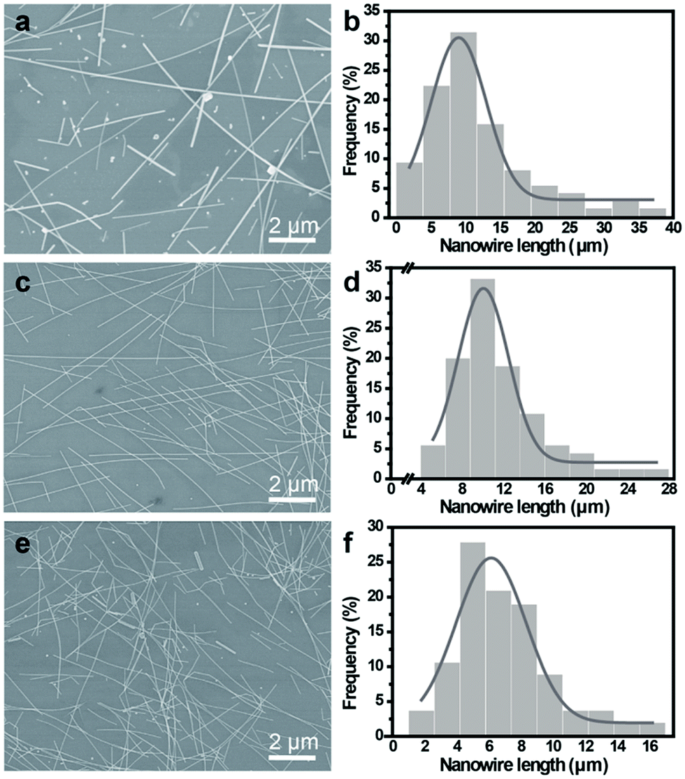 | ||
| Fig. 3 SEM images and length distribution of Ag NWs prepared at different stirring speed: (a, b) at 0 rpm the yield of Ag NWs is low, (c, d) at 200 rpm results in high-yield formation of Ag NWs, and (e, f) at 400 rpm Ag NWs with short length are formed. | ||
To evaluate the performance of Ag NW conductors, Ag NW films were fabricated by the spin-coating method on glass substrates. Fig. 4a shows the relationship between the transmittance and sheet resistances of the Ag NW films under ambient conditions. With ultra-thin Ag NWs prepared at 200 rpm, the sheet resistance and transmittance were 106.6 Ω sq−1 and 95.1% at 550 nm, respectively. A low sheet resistance of approximately 26 Ω sq−1 at 90.5% and 12.2 Ω sq−1 at 83.3% was obtained, which are superior to traditional ITO conductor and previously reported Ag NW conductors (20 Ω sq−1 @ 80% at 550 nm7,33 and 19 Ω sq−1 @ 80% at 550 nm (ref. 11)). It is well known that the transmittance depends on the total area covered with Ag NWs on the substrate, hence, the transmittance loss of visible light owing to Ag NWs is approximately equal to the total area covered with the Ag NWs and the density dependence of the optical transmittance of an Ag NW film can be given by the following equation.33
| % T = 100 × (1 − Ac) | (1) |
| Ac = Ld | (2) |
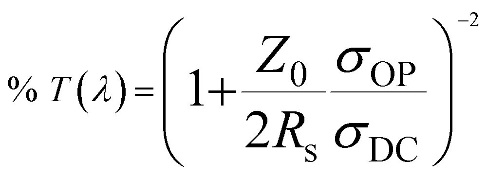 | (3) |
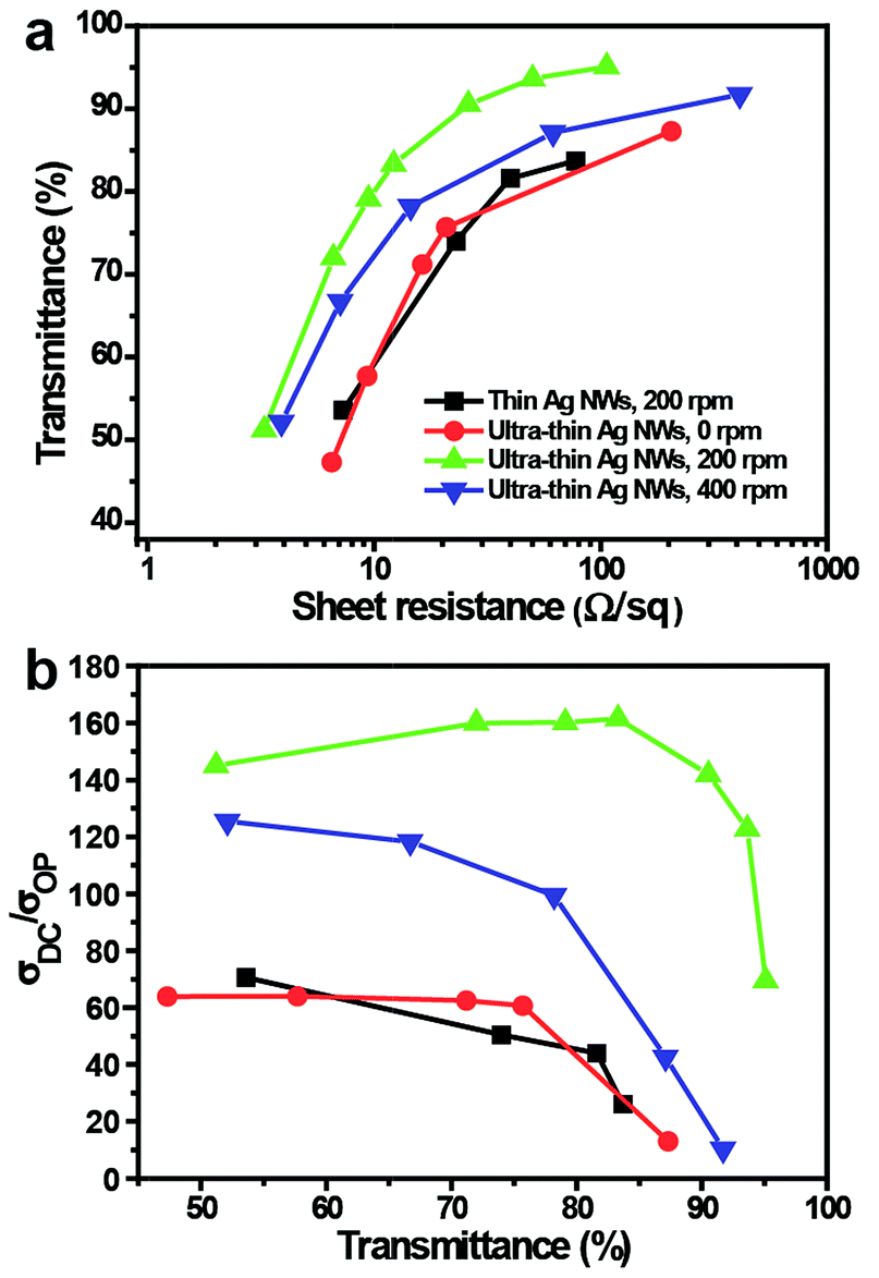 | ||
| Fig. 4 (a) Measured Rs–T performance of transparent Ag NW conductors and (b) comparison of their corresponding σDC/σOP. | ||
Haze is crucial in display applications where scattering will reduce the sharpness of an image, the haze factor of a transparent conducting films extremely dependent on nanowire diameter, with lower diameter nanowires featuring less haze.17 We tested the haze of different diameter Ag NW films and Fig. 5 shows several haze values at different total transmittance values. The haze value decreased almost linearly with the increase of total transmittance for different diameter Ag NW films. For ultrathin Ag NW films, the total transmittance is 91.6%, and the haze factor is about 2%, at total transmittance of 95.7%, the haze factor is only 0.96%. With the decrease of the diameter of the Ag NWs, the haze value increased at the same total transmittance. Compare to large diameter Ag NWs, the ultrathin Ag NW based films show lower haze and our result for ultrathin Ag NW films also showed significantly lower haze than any other Ag NW transparent conductor reported in the literature.
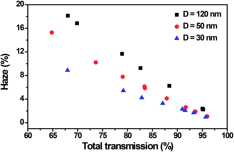 | ||
| Fig. 5 The relationship between the haze and total transmission for different diameter Ag NW films. The conductors with ultrathin Ag NWs showed low haze of 2% and 91.6% T at wavelength of 550 nm. | ||
In summary, the effect of initial nucleation source and the stirring speeds for Ag NW synthesis through polyol method was studied. Compared to traditional polyol methods, reducing silver nitrate by using AgCl and NaBr as nucleation of silver seed results in rapid synthesis of ultrathin Ag NWs. Meanwhile, by adjusting the speed of the magnetic stirring, the yield of ultrathin Ag NW increased significantly, with a high value of 90%. The produced Ag NWs exhibit an average diameter of 30 nm and an average length of 11 μm. By using the above nanowires, high performance Ag NW films with low sheet resistance and ultrahigh transmittance were achieved. The obtained Ag NW conductor exhibits a sheet resistance of 26 Ω sq−1 at 90.5% and of 12.2 Ω sq−1 at 83.3%. A value of σDC/σOP = 162 is large enough for Ag NW conductors. Moreover, ultrathin Ag NW conductor exhibits a low haze of 2% and a low sheet resistance of 30 Ω sq−1 at a high optical transmittance of 91.6%. The haze factor is 0.96% at a transmittance of 95.7%. Such high-yield and rapid synthesis of ultrathin Ag NWs through the modified polyol method show great potential application in flexible electronics of the very near future.
Acknowledgements
This work was supported by the National Key Basic Research Program of China (973 Program, 2015CB932200), the National Natural Science Funds for Excellent Young Scholars (61622402), the National Natural Science Foundation of China (61376088, 51302134, 51528201), Natural Science Foundation of Jiangsu Higher Education Institutions (13KJB510012), the Natural Science Foundation of Jiangsu Province (BK20130934), and the Six Talent Plan (2015XCL015).Notes and references
- P. C. Hsu, S. Wang, H. Wu, V. K. Narasimhan, D. Kong, H. R. Lee and Y. Cui, Nat. Commun., 2013, 4, 2522 CrossRef PubMed.
- J. Liang, L. Li, K. Tong, Z. Ren, W. Hu, X. Niu, Y. Chen and Q. Pei, ACS Nano, 2014, 8, 1590 CrossRef CAS PubMed.
- H. Guo, N. Lin, Y. Chen, Z. Wang, Q. Xie, T. Zheng, N. Gao, S. Li, J. Kang, D. Cai and D. L. Peng, Sci. Rep., 2013, 8, 421 Search PubMed.
- J. Jiu, T. Araki, J. Wang, M. Nogi, T. Sugahara, S. Nagao, H. Koga, K. Suganuma, E. Nakazawa, M. Hara, H. Uchida and K. Shinozaki, J. Mater. Chem. A, 2014, 2, 6326 CAS.
- H. Kang, S. Jung, S. Jeong, G. Kim and K. Lee, Nat. Commun., 2015, 6, 6503 CrossRef CAS PubMed.
- M. S. Lee, K. Lee, S. Y. Kim, H. Lee, J. Park, K. H. Choi, H. K. Kim, D. G. Kim, D. Y. Lee, S. W. Nam and J. U. Park, Nano Lett., 2013, 13, 2814 CrossRef CAS PubMed.
- L. Hu, H. S. Kim, J. Y. Lee, P. Peumans and Y. Cui, ACS Nano, 2010, 4, 2955 CrossRef CAS PubMed.
- H. G. Lm, S. H. Jung, J. Jin, D. Lee, J. Lee, D. Lee, J. Y. Lee, I. D. Kim and B. S. Bae, ACS Nano, 2014, 8, 10973 CrossRef PubMed.
- J. Song, J. Li, J. Xu and H. Zeng, Nano Lett., 2014, 14, 6298 CrossRef CAS PubMed.
- J. Y. Lee, S. T. Connor, Y. Cui and P. Peumans, Nano Lett., 2008, 8, 689 CrossRef CAS PubMed.
- T. Araki, J. Jiu, M. Nogi, H. Koga, S. Nagao, T. Sugahara and K. Suganuma, Nano Res., 2014, 7, 236 CrossRef CAS.
- T. Kim, A. Canlier, G. H. Kim, J. Choi, M. Park and S. M. Han, ACS Appl. Mater. Interfaces, 2013, 5, 788 CAS.
- C. Preston, Y. Xu, X. Han, J. N. Munday and L. Hu, Nano Res., 2013, 6, 461 CrossRef CAS.
- J. Y. Lin, Y. L. Hsueh and J. J. Huang, J. Solid State Chem., 2014, 214, 2 CrossRef CAS.
- J. Y. Lin, Y. L. Hsueh, J. J. Huang and J. R. Wu, Thin Solid Films, 2015, 584, 243 CrossRef CAS.
- R. Yang, C. Sui, J. Gong and L. Qu, Mater. Lett., 2007, 61, 900 CrossRef CAS.
- C. J. Murphy and N. R. Jana, Adv. Mater., 2002, 14, 80 CrossRef CAS.
- J. Lee, P. Lee, H. Lee, D. Lee, S. S. Lee and S. H. Ko, Nanoscale, 2012, 4, 6408 RSC.
- P. Lee, J. Lee, H. Lee, J. Yeo, S. Hong, K. H. Nam, D. Lee, S. S. Lee and S. H. Ko, Adv. Mater., 2012, 24, 3326 CrossRef CAS PubMed.
- T. Tokuno, M. Nogi, J. Jiu and K. Suganuma, Nanoscale Res. Lett., 2012, 7, 281 CrossRef PubMed.
- S. De, T. M. Higgins, P. E. Lyons, E. M. Doherty, P. N. Nirmalraj, W. J. Blau, J. J. Boland and J. N. Coleman, ACS Nano, 2009, 3, 1767 CrossRef CAS PubMed.
- J. Jiu, K. Murai, D. Kim, K. Kim and K. Suganuma, Mater. Chem. Phys., 2009, 114, 333 CrossRef CAS.
- W. Gaynor, G. F. Burkhard, M. D. McGehee and P. Peumans, Adv. Mater., 2011, 23, 2905 CrossRef CAS PubMed.
- J. Jiu, M. Nogi, T. Sugahara, T. Tokuno, T. Araki, N. Komoda, K. Suganuma, H. Uchidab and K. Shinozaki, J. Mater. Chem., 2012, 22, 23561 RSC.
- E. J. Lee, M. H. Chang, Y. S. Kim and J. Y. Kim, APL Mater., 2013, 1, 042118 CrossRef.
- S. M. Bergin, Y. H. Chen, A. R. Rathmell, P. Charbonneau, Z. Y. Li and B. J. Wiley, Nanoscale, 2012, 4, 1996 RSC.
- X. Tang, M. Tsuji, P. Jiang, M. Nishio, S. M. Jang and S. H. Yoon, Colloids Surf., A, 2009, 338, 33 CrossRef CAS.
- Q. Zhang, Y. Hu, S. Guo, J. Goebl and Y. Yin, Nano Lett., 2010, 10, 5037 CrossRef CAS PubMed.
- Y. J. Song, M. Wang, X. Y. Zhang, J. Y. Wu and T. Zhang, Nanoscale Res. Lett., 2014, 9, 17 CrossRef PubMed.
- J. P. Kottmann, O. J. F. Martin, D. R. Smith and S. Schultz, Phys. Rev. B: Condens. Matter Mater. Phys., 2001, 64, 235402 CrossRef.
- Y. Sun and Y. Xia, Analyst, 2003, 128, 686 RSC.
- J. J. Mock, S. J. Oldenburg, D. R. Smith, D. A. Schultz and S. Schultz, Nano Lett., 2002, 2, 465 CrossRef CAS.
- S. E. Park, S. Kim, D. Y. Lee, E. Kim and J. Hwang, J. Mater. Chem. A, 2013, 1, 14286 CAS.
- A. G. Acosta, A. M. Ramírez, E. J. L. Naranjo, L. M. Apatiga, R. H. Basurto and E. M. R. Muñoz, Mater. Lett., 2015, 138, 167 CrossRef.
- M. G. Dressel and G. Gruner, Electrodynamics of Solids: Optical properties of Electrons in Matter, Cambridge University Press, Cambridge, 2002 Search PubMed.
- W. He and C. Ye, J. Mater. Sci. Technol., 2015, 31, 581 Search PubMed.
- K. Zhang, Y. Du and S. Chen, Org. Electron., 2015, 26, 380 CrossRef CAS.
- Y. H. Duan, Y. Duan, X. Wang, D. Yang, Y. Q. Yang, P. Chen, F. B. Sun, K. W. Xue and Y. Zhao, Appl. Surf. Sci., 2015, 351, 445 CrossRef CAS.
Footnote |
| † Electronic supplementary information (ESI) available. See DOI: 10.1039/c6ra27760h |
| This journal is © The Royal Society of Chemistry 2017 |