
 Open Access Article
 This Open Access Article is licensed under a
 Creative Commons Attribution 3.0 Unported Licence
Enhanced light–matter interaction of a MoS2 monolayer with a gold mirror layer
Haifeng Xu *
*
School of Mechanical and Electronic Engineering, Suzhou University, Suzhou 234000, PR China. E-mail: xuhaifeng@ahsztc.edu.cn
First published on 26th April 2017
Abstract
MoS2 monolayer is a member of transition metal dichalcogenides (TMDs), which has shown great potential for applications in light-emitting devices due to a direct band gap in its electronic structure. However, a region of atmomic thickness remains a challenge due to its weak light-matter interaction. Most approaches to improve the light–matter interaction of MoS2 have been devoted to plasmonic nanostructures and photonic crystal. Herein, we demonstrated a method based on the insertion of a gold mirror layer between the dielectric layer and the substrate to enhance the optical absorption and emission of the MoS2 monolayer. The hybrid nanostructure comprised a 35 nm SiO2 dielectric spacer and 40 nm golden film. The overall photoluminescence intensity was amplified nearly 4 times, resulting from enhanced optical absorption and Fabry–Perot cavity reflection. We further demonstrated that the improvement in the PL intensity can also be modulated by selecting a spacer material and changing the layer thickness. This study is broadly applicable to enhance the light–matter interaction of TMDs for applications in potential devices such as light-emitting devices, lasers, and photodetectors.
Introduction
Two-dimensional (2D) materials with a direct band gap provide great opportunities for novel optoelectronic devices involving phototransistor,1,2 light-emitting device,3–5 and nanolaser.6 As a member of transition metal dichalcogenide (TMD) family, MoS2 monolayer is a direct band gap semiconductor;7 it exhibits intriguing physics in light-emitting properties such as multi-exciton recombination,8,9 valley polarization PL,10,11 and tunable band gap emission.12,13 Despite the fact that the large absorption coefficients of the MoS2 monolayer are efficient, the low quantum efficiency of MoS2 monolayer in an atomically thin region limits its development in high-performance optoelectronic devices. Great efforts have been devoted for the modulation of optical absorption and light emission of the MoS2 monolayer. The PL intensity of the MoS2 monolayer is drastically enhanced by the adsorption of p-type dopants (F4TCNQ and TCNQ), which depends on the switching of exciton and trion competition with doping charges.14 Its PL in a designed electromechanical device can be increased up to 200% for an applied strain of ∼0.2%.12 Because of the photonic crystal cavities with low loss and strong field restriction, the laser light can be pumped at a low-threshold.6,15 Plasmonic nanoparticles under resonant excitation cause huge electric field enhancement and hot-electron injection, resulting in extreme enhancement of PL.16,17 However, most of the techniques acquire precise fabrication processing that cannot realize large-scale device integration.In this study, we demonstrated that a mirror layer in a substrate played a significant role in the optical gain of the MoS2 monolayer. MoS2 monolayers were successfully transferred onto SiO2/Si and SiO2/Au/Si substrates via wetting transfer technology. The spectral change due to different substrates was systematically investigated to elaborate the mechanism of the mirror layer-enhanced light–matter interaction. The absorption spectra were dramatically improved in the case of a hybrid substrate consisting of 35 nm SiO2 and a 40 nm gold mirror layer, which was due to Fabry–Perot interference-induced multi-reflection light absorption. Moreover, the exciton recombination rate was dramatically increased with the field enhancement, resulting in a 4-fold PL enhancement of MoS2 on the hybrid substrate. We proposed that by performing electromagnetic simulations, light–matter interaction of MoS2 monolayer can be engineered by selecting the spacer material and spacer thickness for broadband system. This study provides an opportunity to optimize the light–matter interaction of 2D materials and further improve the performance of 2D optoelectronic devices.
Results
Schematics of the optical propagation on the hybrid structure containing chemical vapor deposition (CVD)-grown MoS2 monolayer and hybrid substrate are presented in Fig. 1a and b. Fig. 1a shows the schematic of the MoS2 monolayer on the SiO2/Si substrate, wherein most of the light indirectly passed through the dielectric layer and reached the interface of SiO2/Si. The poor reflection induced by the Si substrate was neglected. However, when a gold mirror layer was inserted between the dielectric and metal layer, the Fabry–Perot cavities were induced, resulting in multi-reflection and absorption. When the incident light illuminated the hybrid structure, a fraction of the incident light was absorbed by the MoS2 monolayer and most of the light was transmitted further into the dielectric layer. The transmittance light reached the interface of the Au film and reflected at the metal surface, referred as the mirror effect. Moreover, the reflected light was partially absorbed on MoS2 and reflected at the MoS2/SiO2 interface.18 The repetition of absorption and reflection eventually increased the light–matter interaction of the MoS2 monolayer. The entire process of light–matter interaction in the MoS2 monolayer can be understood as follows: MoS2 absorbed photogenerated free electrons and holes, electrons (holes) relaxed to the bottom (top) conduction (valence) band, and formed excitons, emitting PL.19 Besides the effect of Fabry–Perot interference, the rough Au film would also generate field enhancement due to the plasmonic effect, which may increase exciton recombination efficiency, contributing to PL enhancement.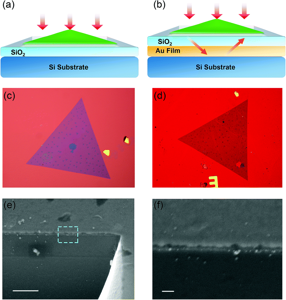 | ||
| Fig. 1 Optical characteristics of MoS2 without and with metal films. (a) Schematic of the absorption and PL of MoS2 on the SiO2/Si substrate. (b) Schematic of the absorption and PL of MoS2 on the SiO2/Au/Si substrate. (c) Image of the MoS2 monolayer on the SiO2/Si substrate. (d) Image of the MoS2 monolayer on the SiO2/Au/Si substrate. (e) SEM image of the cut cross-section of the substrate; scale bar is 300 nm. (f) High resolution SEM image of the cross-section of the substrate within the dotted line shown in (e); scale bar is 30 nm. | ||
Fig. 1c and d show the optical images of the MoS2 monolayer transferred on different substrates. CVD-grown MoS2 on the 35 nm SiO2/Si substrate can be clearly observed as the blue triangular region, and some dark blue dots were the two-layered MoS2 domains.20 The color of the MoS2 monolayer was dark red with poor optical contrast, which was related to the Fabry–Perot interference. The side length of the triangular MoS2 monolayer was about 100 μm, and some wrinkles and defects were caused during the transfer process. The properties of the substrates, as shown in Fig. 1e and d, were studied at the tilted view of 45°, where a cross section of the substrate was cut using focused ion beam (FIB) with a Ga source. The hybrid layer of 30 nm SiO2 and 40 nm Au was clearly observed as the dotted region shown in Fig. 1e at low resolution, and the scale bar is 300 nm. The dotted region was amplified using a high magnification objective lens, as shown in Fig. 1f, with the scale bar of 30 nm. The Au layer is a conductive film and appears as a bright layer in the SEM image. Although the surface was slightly rough, the average thicknesses of SiO2 and Au were about 35 nm and 40 nm, respectively.
The MoS2 monolayer samples were grown via a chemical vapor deposition (CVD) method.21 The sulfur (S) and molybdenum oxide (MoO3) powder were prepared as the S and Mo source, respectively. The S powder was located at the upstream region of the furnace, and the MoO3 powder in a grown boat was placed in a fused quartz tube at the center of the CVD furnace. The samples were first grown on a 300 nm SiO2/Si substrate and were transferred onto the prepared substrates via a wetting transfer process. The SiO2 film and Au film were both deposited using an e-beam deposition system. A home-built spectrometer was used for obtaining Raman and PL spectra using an iHR550 Raman spectrometer (Horiba) and a CCD imaging system. The objective lens had 50× magnification, and the excitation laser wavelength was 488 nm. The working gratings were 600 g mm−1 for PL detection and 2400 g mm−1 for high resolution Raman acquisition. Fig. 2a shows the Raman spectra of the MoS2 monolayer on the SiO2/Au/Si substrate. The E12g peak was obtained at 389.0 cm−1, representing in-plane vibrations, and the A1g mode peak was acquired at 410.3 cm−1, representing the out-of-plane mode. The difference in the characteristic frequency between E12g and A1g phonon modes of the MoS2 structure was determined to be 20.7 cm−1.22 From both the optical image contrast and Raman frequency difference, the samples were verified as monolayers. A Raman peak map of the MoS2 monolayer integrated at the A1g mode is shown in Fig. 2b, confirming the homogeneous properties of the CVD-grown samples.
 | ||
| Fig. 2 Raman spectra of MoS2 on the hybrid substrate with metal films. (a) Raman intensity of the MoS2 monolayer on the prepared substrate. (b) Raman map of the MoS2 monolayer integrated at the A1g mode. | ||
The spectral properties of the MoS2 monolayer on different substrates were further investigated, and the results are shown in Fig. 3. Fig. 3a shows the optical absorption of the MoS2 monolayer on different substrate, and the thickness of the MoS2 monolayer was about 0.7 nm. The overall spectral intensity (red line) significantly enhanced on the SiO2/Au substrate with the obvious exciton A and B peaks near 660 nm and 615 nm, respectively. When the MoS2 monolayer was placed on the substrate without a gold mirror layer, no clear spectral peak was observed due to poor absorption. The maximum enhancement of optical absorption was nearly 6-fold, and this contrast could be attributed to the Fabry–Perot cavity. Fig. 3b shows the difference in the absorption cross-section simulated by (Finite-Difference Time-Domain) FDTD solutions. The dielectric constant of the MoS2 monolayer was utilized by parameterizing the experimental data into a band exciton transition (BET) model, as reported in the previous work.23 The absorption cross section of the MoS2 monolayer was enhanced more than two times, which was simulated by FDTD solutions and corresponded to the experimental phenomenon. Because of the absorbance enhancement, light–matter interaction was increased. This generated more exciton in the band gap. Therefore, PL intensity dramatically amplified under the 488 nm excitation laser.
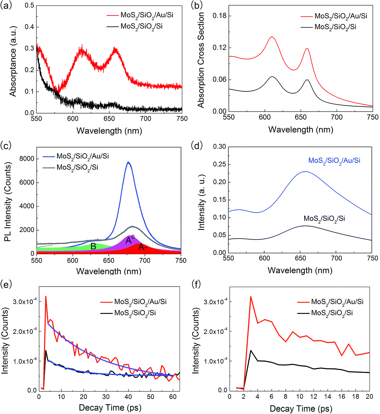 | ||
| Fig. 3 Enhanced optical absorption and PL intensity of MoS2 with a metallic mirror layer. (a) Absorption spectra of the MoS2 monolayer on different substrates. (b) Simulations on enhanced absorption cross-section of the MoS2 monolayer on different substrates. (c) PL spectra of the MoS2 monolayer on different substrates. (d) Simulations of the electric field intensity on different substrates. (e) Ultrafast signals and fitting curves of the MoS2 monolayer on different substrates under a pump fluence of 13.2 μJ cm−2. The wavelengths of the pump and probe are 400 and 675 nm, respectively. (f) Detailed signals of the MoS2 monolayer. | ||
As shown in Fig. 3c, total PL intensity increased nearly 4-fold with the laser power of 1.6 mW. The main PL peak is composed of primary exciton A0, trion A− (two electrons bounding a hole), and valence band splitting-induced B exciton. The peak energy of the exciton A0, exciton A−, and exciton B was fitted by Lorenz peaks near 1.83 eV (678 nm), 1.80 eV (689 nm), and 1.96 eV (633 nm), respectively.24 Moreover, the binding energy of the exciton A0 is ∼40 meV, which agrees with the value reported earlier. In addition, the spectral shape of the MoS2 monolayer was further altered with the gold mirror layer, which was due to the selective amplification of the primary exciton A0. Moreover, the intensity of exciton recombination was obviously attenuated, as shown in the fitting curves of Fig. 3c. Fig. 3d shows the electric field enhancement at the surface of the substrate, where the exciton was treated as the dipole radiation source. The electric field was increased nearly three times, as observed from FDTD simulations.
In a dipole–dielectric–metal structure model, the dipole emission is directly associated with the electric-field enhancement, which is known as the Purcell effect. The Purcell enhancement factor can be defined as FP ≡ Γ1/Γ0,25 where Γ1 and Γ0 are the radiative decay rates on SiO2/Si and SiO2/Au/Si substrates, respectively. Basically, Γ is directly proportional to the square of electric (E) and electric dipole (d). Fig. 3e and f show the ultrafast pump–probe signals of the MoS2 monolayer on different substrates. In the ultrafast pump–probe measurement, wavelengths of pump and probe were 400 and 675 nm, respectively. A 100 fs laser pulse with a pump fluence of 13.2 μJ cm−2 excited the electron–hole pairs in the MoS2 monolayer. The decay signals could be fitted by decay functions, as expressed by y = y0 + Ae(−t/τ), wherein the emission rate can be estimated from the experimental results. The decay rates of MoS2 on different substrates were obtained as 25.6 ps (Γ1) and 11.1 ps (Γ0). As the emission rate Γ1 was larger than Γ0, the spontaneous emission of MoS2 monolayer was enhanced and restricted the formation of trion and exciton B due to limited band-filling effect.18,26 In MoS2 semiconductor, hot carriers excited by laser illumination were thermalized to the lowest exciton energy level and recombined via radiative or nonradiative decay. Under intense light, when the optical carrier generation rate was much lower than the recombination rate, thermalized carriers accumulated from the band edge and quasi-Fermi level shifted deeper into the conduction and valence bands in a steady state. Although multi-reflection strengthens the light–matter interaction of the MoS2 monolayer, providing more excitons, there were still not enough excitons to fill the exciton states due to field enhanced emission rate. Moreover, MoS2 primary exciton emission was selectively amplified, which resulted in the overall PL enhancement.
To systematically investigate the enhancement of the light–matter interaction of the MoS2 monolayer via Fabry–Perot interference, simulations of electric field and optical absorption depending on mirror materials and dielectric layer thickness were conducted at normal light incidence. In the present study, Fabry–Perot interference originated from multiple interfaces among air/SiO2 and SiO2/Au contact surface, indicating destructive and constructive interference in the SiO2 layer. In Fig. 4a, Si substrate, metal film (40 nm), and SiO2 layer (35 nm) were stacked in adjacent regime from bottom to top along vertical direction. The MoS2 monolayer was located at the surface of the SiO2 layer. The calculated map of the electric field intensity (|E|2) is displayed in the x–z plane with the normal incident light wavelength of 680 nm. The resulting |E|2 profiles in air were found oscillatory along the z direction with a period of 340 nm. The refractive index of air, SiO2, Au at 680 nm was considered as 1, 1.5, and 0.2, respectively. The dependence on the metal materials was further investigated among Al, Au, Ag, and Cu. The layer thickness was set constant, and the calculated electric field intensities (|E|2) on the surface of the SiO2 layer are shown in Fig. 3b. The intensity increased in the order of Ag, Cu, Au, and Al because Ag exhibited ultra-low dissipation and strong reflectance in the visible range. A proper mirror material in the proposed substrate can be optimized to achieve strong light–matter interaction of the MoS2 monolayer.
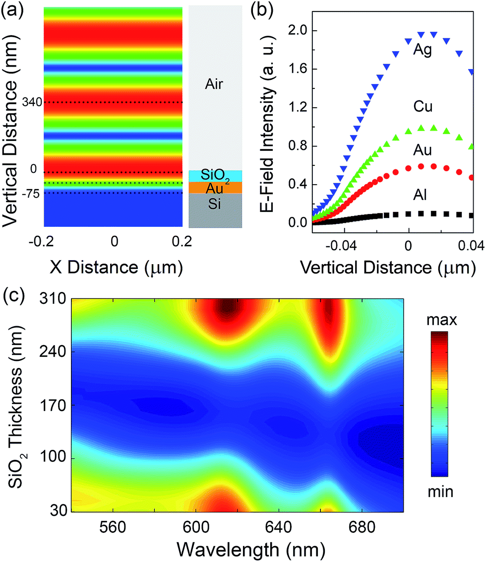 | ||
| Fig. 4 Investigation on the mirror materials and dielectric thickness. (a) Electromagnetic field profile across 35 nm of SiO2, 40 nm of Au film, and air, stacked in sequence. (b) Electric field intensity as a function of vertical distance. (c) Absorption of the MoS2 monolayer on the SiO2 surface layer having various thicknesses . | ||
In the classical Fabry–Perot cavity, constructive interference occurred at the condition 2nd cos![[thin space (1/6-em)]](https://www.rsc.org/images/entities/char_2009.gif) θ = mλ, where n = 1.5 is the refractive index of SiO2 between two mirror surfaces, d = 35 nm is the thickness of the SiO2 layer, θ is the angle of the incident light measured from the vertical line against the reflecting surface, m is the order of interference, and λ = 680 nm is the wavelength of the radiation in vacuum. The separation difference between two consecutive constructive interferences (m = 1) was estimated to be 226 nm (Δd ≈ λ/3). However, the interference condition was different in the current case because there was only one metallic reflecting layer at one side. The simulations of MoS2 absorption at the surface can be performed to optimize the results. Fig. 4c shows the map of MoS2 absorption intensity distribution from 540 to 700 nm, which was plotted with different thickness of the SiO2 layer ranging from 30 to 310 nm. All the substrates with 30–40 nm and 240–310 nm SiO2 film showed dramatic enhancement of both absorption peaks. There appears a period of absorption maximum, which is consistent with the changing order of the diffraction of the Fabry–Perot interference. These results can be applied for improving the light–matter interaction of 2D materials by designing a hybrid substrate.
θ = mλ, where n = 1.5 is the refractive index of SiO2 between two mirror surfaces, d = 35 nm is the thickness of the SiO2 layer, θ is the angle of the incident light measured from the vertical line against the reflecting surface, m is the order of interference, and λ = 680 nm is the wavelength of the radiation in vacuum. The separation difference between two consecutive constructive interferences (m = 1) was estimated to be 226 nm (Δd ≈ λ/3). However, the interference condition was different in the current case because there was only one metallic reflecting layer at one side. The simulations of MoS2 absorption at the surface can be performed to optimize the results. Fig. 4c shows the map of MoS2 absorption intensity distribution from 540 to 700 nm, which was plotted with different thickness of the SiO2 layer ranging from 30 to 310 nm. All the substrates with 30–40 nm and 240–310 nm SiO2 film showed dramatic enhancement of both absorption peaks. There appears a period of absorption maximum, which is consistent with the changing order of the diffraction of the Fabry–Perot interference. These results can be applied for improving the light–matter interaction of 2D materials by designing a hybrid substrate.
Conclusion
In summary, the mechanism of mirror layer-enhanced light–matter interaction of the MoS2 monolayer was systematically investigated via optical absorption, PL, and Raman spectra. Incident light transmitted into the SiO2 film, reflected at the interface of SiO2/Au, and returned to the surface of the SiO2 layer, resulting in multiple light reflection in the Fabry–Perot cavity. The enhancement of exciton absorption was nearly 6-fold due to multi-reflection-induced optical absorption. MoS2 PL was selectively amplified more than 4 times, which was consistent with electromagnetic simulations by FDTD solutions. The primary exciton was selectively amplified due to enhanced light–matter interaction and band filling effect and totally changed the PL spectral shape. Furthermore, the role of metal materials and dielectric layer thickness were analyzed in detail, and these could be applied for choosing an optimized hybrid substrate to achieve light–matter enhancement in 2D materials. This study provides a simple and practical way for enhancing the light–matter interaction of 2D materials compatible for applications in large-scale optoelectronic devices such as LEDs, photodetectors, solar cells, and lasers.Acknowledgements
This work was financially supported by Natural Science Foundation of Anhui Province (Grant no. 148085QA20, and 1508085ME104), Natural Science Key Foundational of Anhui Province (Grant no. KJ2015A210, and KJ2015A250), Anhui Province Outstanding Young Talent Support Program (Grant no. GXYQ2017094), Anhui Provincial Key Research and Development Program (Grant no. 1704A0902022), Science Foundation of Suzhou University (Grant no. 2015JB06). We thank Dr Wei Li in Beijing Normal University for detecting pump–probe detection.References
- O. Lopez-Sanchez, D. Lembke, M. Kayci, A. Radenovic and A. Kis, Nat. Nanotechnol., 2013, 8, 497–501 CrossRef CAS PubMed.
- J. Lin, H. Li, H. Zhang and W. Chen, Appl. Phys. Lett., 2013, 102, 203109 CrossRef.
- R. S. Sundaram, M. Engel, A. Lombardo, R. Krupke, A. C. Ferrari, P. Avouris and M. Steiner, Nano Lett., 2013, 13, 1416–1421 CrossRef CAS PubMed.
- K. F. Mak, K. He, C. Lee, G. H. Lee, J. Hone, T. F. Heinz and J. Shan, Nat. Mater., 2013, 12, 207–211 CrossRef CAS PubMed.
- W. Yang, J. Shang, J. Wang, X. Shen, B. Cao, N. Peimyoo, C. Zou, Y. Chen, Y. Wang, C. Cong, W. Huang and T. Yu, Nano Lett., 2016, 16, 1560–1567 CrossRef CAS PubMed.
- S. Wu, S. Buckley, J. R. Schaibley, L. Feng, J. Yan, D. G. Mandrus, F. Hatami, W. Yao, J. Vuckovic, A. Majumdar and X. Xu, Nature, 2015, 520, 69–72 CrossRef CAS PubMed.
- K. F. Mak, C. Lee, J. Hone, J. Shan and T. F. Heinz, Phys. Rev. Lett., 2010, 105, 136805 CrossRef PubMed.
- A. Newaz, D. Prasai, J. Ziegler, D. Caudel, S. Robinson, R. Haglund Jr and K. Bolotin, Solid State Commun., 2013, 155, 49–52 CrossRef CAS.
- J. S. Ross, S. Wu, H. Yu, N. J. Ghimire, A. M. Jones, G. Aivazian, J. Yan, D. G. Mandrus, D. Xiao, W. Yao and X. Xu, Nat. Commun., 2013, 4, 1474 CrossRef PubMed.
- T. Cao, G. Wang, W. Han, H. Ye, C. Zhu, J. Shi, Q. Niu, P. Tan, E. Wang, B. Liu and J. Feng, Nat. Commun., 2012, 3, 887 CrossRef PubMed.
- H. Zeng, J. Dai, W. Yao, D. Xiao and X. Cui, Nat. Nanotechnol., 2012, 7, 490–493 CrossRef CAS PubMed.
- Y. Y. Hui, X. Liu, W. Jie, N. Y. Chan, J. Hao, Y. T. Hsu, L. J. Li, W. Guo and S. P. Lau, ACS Nano, 2013, 7, 7126–7131 CrossRef CAS PubMed.
- K. He, C. Poole, K. F. Mak and J. Shan, Nano Lett., 2013, 13, 2931–2936 CrossRef CAS PubMed.
- S. Mouri, Y. Miyauchi and K. Matsuda, Nano Lett., 2013, 13, 5944–5948 CrossRef CAS PubMed.
- X. Liu, T. Galfsky, Z. Sun, F. Xia, E.-c. Lin, Y.-H. Lee, S. Kéna-Cohen and V. M. Menon, Nat. Photonics, 2014, 9, 30–34 CrossRef.
- Z. Wang, Z. Dong, Y. Gu, Y. H. Chang, L. Zhang, L. J. Li, W. Zhao, G. Eda, W. Zhang, G. Grinblat, S. A. Maier, J. K. Yang, C. W. Qiu and A. T. Wee, Nat. Commun., 2016, 7, 11283 CrossRef CAS PubMed.
- G. M. Akselrod, T. Ming, C. Argyropoulos, T. B. Hoang, Y. Lin, X. Ling, D. R. Smith, J. Kong and M. H. Mikkelsen, Nano Lett., 2015, 15, 3578–3584 CrossRef CAS PubMed.
- H. Y. Jeong, U. J. Kim, H. Kin, G. H. Han, L. Hyangsook, M. S. Kim, Y. Jin, T. H. Ly, S. Y. Lee, Y.-G. Roh, W.-J. Joo, S. W. Hwang, Y. Park and Y. H. Lee, ACS Nano, 2016, 10, 8192–8198 CrossRef CAS PubMed.
- H. S. Lee, M. S. Kim, Y. J. Jin, G. H. Han, Y. H. Lee and J. Kim, Phys. Rev. Lett., 2015, 115, 226801 CrossRef PubMed.
- M. M. Benameur, B. Radisavljevic, J. S. Heron, S. Sahoo, H. Berger and A. Kis, Nanotechnology, 2011, 22, 125706 CrossRef CAS PubMed.
- S. Najmaei, Z. Liu, W. Zhou, X. Zou, G. Shi, S. Lei, B. I. Yakobson, J. C. Idrobo, P. M. Ajayan and J. Lou, Nat. Mater., 2013, 12, 754–759 CrossRef CAS PubMed.
- Z. Li, R. Ye, R. Feng, Y. Kang, X. Zhu, J. M. Tour and Z. Fang, Adv. Mater., 2015, 27, 5235–5240 CrossRef CAS PubMed.
- J.-T. Liu, T.-B. Wang, X.-J. Li and N.-H. Liu, J. Appl. Phys., 2014, 115, 193511 CrossRef.
- C. Zhang, H. Wang, W. Chan, C. Manolatou and F. Rana, Phys. Rev. B, 2014, 89, 205436 CrossRef.
- H. Nan, Z. Wang, W. Wang, Z. Liang, Y. Lu, Q. Chen, D. He, P. Tan, F. Miao and X. Wang, ACS Nano, 2014, 8, 5738–5745 CrossRef CAS PubMed.
- M. J. Shin, D. H. Kim and D. Lim, J. Korean Phys. Soc., 2015, 65, 2077–2081 CrossRef.
| This journal is © The Royal Society of Chemistry 2017 |