
 Open Access Article
 This Open Access Article is licensed under a
 Creative Commons Attribution 3.0 Unported Licence
Sensitivity enhancement of graphene Hall sensors modified by single-molecule magnets at room temperature†
Yuanhui Zheng‡
ab,
Le Huang‡c,
Zhiyong Zhang*c,
Jianzhuang Jiang*d,
Kaiyou Wang*e,
Lian-Mao Peng*c and
Gui Yu *ab
*ab
aBeijing National Laboratory for Molecular Sciences, Institute of Chemistry, Chinese Academy of Sciences, Beijing 100190, P. R. China. E-mail: yugui@iccas.ac.cn
bUniversity of Chinese Academy of Sciences, Beijing 100049, P. R. China
cKey Laboratory for the Physics and Chemistry of Nanodevices, Department of Electronics, Peking University, Beijing 100871, P. R. China. E-mail: zyzhang@pku.edu.cn; lmpeng@pku.edu.cn
dBeijing Key Laboratory for Science and Application of Functional Molecular and Crystalline Materials, Department of Chemistry, University of Science and Technology Beijing, Beijing 100083, P. R. China. E-mail: jianzhuang@ustb.edu.cn
eSKLSM, Institute of Semiconductors Chinese Academy of Sciences, Beijing 100083, P. R. China. E-mail: kywang@semi.ac.cn
First published on 4th January 2017
Abstract
Single-molecule magnets (SMMs) possess many unique magnetic properties and thus attract a wide range of attention. However, the applications of SMMs always need a strict atmosphere, i.e. low temperature, high vacuum and strong magnetic field. In this work, we report the preparation and characterization of sensitivity enhanced graphene Hall elements (GHEs) decorated with Tb-core SMMs. By comparing the magnetic sensing and electronic tests of the GHEs before and after the SMMs modifications, the sensitivity of the GHEs increases by 44.9% in voltage mode and 59.0% in current mode compared with pristine GHEs. The increase of sensitivity may result from the magnetic center introduction of SMMs at room temperature. Moreover, the magnetic molecules may affect the graphene field environment leading to a Hall signal change. In addition, the SMMs modified GHEs present excellent linearity, offset voltage, repeatability and stability in magnetic sensing. This study paves the way to apply SMMs into practical use at room temperature and atmospheric pressure without strong magnetic field excitations.
Introduction
In recent years, single-molecule magnets (SMMs) have been intensively investigated due to their unique magnetic hysteresis and quantum behavior phenomenon under low temperature.1–5 Furthermore, SMMs are considered as a promising material for building quantum computers,6,7 spintronic devices8,9 and magnetic memories.10,11 Generally, SMMs demonstrate ferromagnetic characteristics under low temperature.12 That is why the vast majority of investigations and applications surrounding SMMs were carried out under low temperature.13–15 However, the strict testing environment limits the practical use of SMMs-based devices and circuits. When the temperature exceeds the Curie temperature of SMMs, the SMMs would transfer to paramagnetic characteristics due to the increasing thermal motions excited by the increased temperature.12 Unlike the ferromagnetic materials, the magnetization of paramagnetic materials would have a linear relationship with the external magnetic field.16,17Actually, graphene is a terrific platform for investigating the proximity effect and magnetic properties of SMMs.9,13 This is originated from the ultra-thin body and excellent electronic properties of graphene. On one hand, the extremely high surface–volume ratio of graphene helps to maximize the impact from the surface SMMs-induced effects on graphene.18 On the other hand, the high mobility and conductivity of graphene enable the transfer of SMMs magnetic information into the electronic signals of graphene effectively.13 These two advantages of graphene are essential to confirm the existence and develop the potential applications of SMMs.
At the same time, graphene is regarded as a fabulous material for constructing high-performance Hall sensors.19 Benefitted from the high mobility, thin body, unique band structure, low noise, thermal stability and flexibility of graphene, graphene Hall elements (GHEs) exhibit high sensitivity, resolution, linearity and stability in magnetic detections.19–23 Moreover, the realization of integrating GHEs with silicon Complementary Metal Oxide Semiconductor (CMOS) integrated circuits (ICs) makes GHEs more promising in practical use.21,24
In this work, we report the fabrication and characterization of sensitivity enhanced GHEs decorated with TbPc2 SMMs. Based on this method, the sensitivity of the GHEs increases by 44.9% in voltage mode and 59.0% in current mode compared with pristine GHEs. This may be attributed to the introduction of magnetic center of SMMs at room temperature. In addition, the magnetic molecules can influence the graphene field environment leading to Hall signal change.13 Additionally, the SMM modified GHEs present excellent linearity, offset voltage, repeatability and stability in magnetic sensing.
Experimental section
Fabrication methods of GHEs
Graphene sample was grown by CVD method based on Pt foil substrate.20 Afterwards, the graphene was transferred onto a SiO2 (285 nm)/Si substrate with a bubbling method.20 Electron beam lithography (EBL) based on PMMA was then carried out to pattern the symmetric cross-shaped graphene channel, followed by a reactive ion etching (RIE) process to remove the needless region of graphene. The second EBL process was used to pattern the metal contacts, followed by an electron beam evaporator (EBE) deposition of Ti/Au (5/30 nm) and a standard lift-off process. The electronic and magnetic response data were collected by a Keithly 4200 SCS semiconductor parameter analyser.Preparations and modifications of SMMs
The SMMs deposited on graphene are pyrenyl-substituted heteroleptical bis(phth-alocyaninato) terbium(III) complexes, which is referred as TbPc2 in this work (Fig. 1b). This molecule consists of a single magnetic ion (Tb3+) coordinated to two phthalocyanine ligands (see scheme of Fig. 1a). In order to improve the adhesion to graphene, one of the two phthalocyanine macrocycles was substituted by a pyrene group. The pyrene group exhibits an attractive interaction with sp2 carbon materials, maximizing the intermolecular interaction.25 The molecule was deposited by drop casting of a TbPc2 solution in dichloromethane (DCM) with a molecule concentration ranging from 10−7 to 10−3 mol L−1. After 10 seconds, the sample was rinsed in DCM for 1 minute to remove the DCM. Afterwards, residual DCM was removed by a second rinse in isopropanol. Finally, the sample was dried by nitrogen flow.26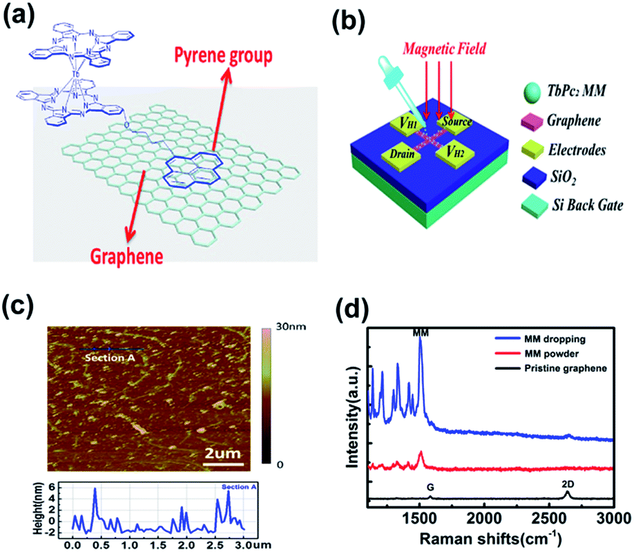 | ||
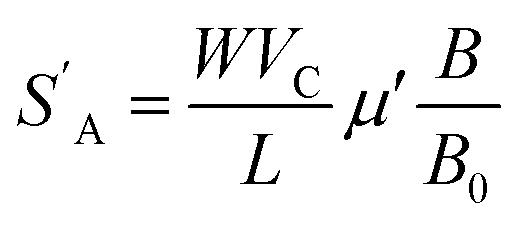
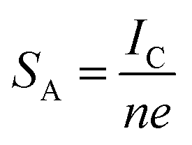
| Fig. 1 Graphene-Single Molecular Magnets (SMMs) hybrid structure and characterizations. (a) Schematic view of TbPc2 molecule attached to graphene. The magnetic core is Tb3+. One of the terminal ligands is substituted by a pyrene group. (b) Schematic of graphene Hall elements (GHEs) decorated with SMMs. The channel length and width are 50 and 15 μm, respectively. The concentration of SMMs is 10−7 mol L−1. (c) Atomic force microscope (AFM) image of SMM-modified graphene. The scale bar is 2 μm. The concentration of SMMs is 10−7 mol L−1. (d) Raman spectrum of the pristine graphene (bottom, black), TbPc2 powder (middle, red), and the hybrid system of graphene and TbPc2 SMMs (top, blue). The G and 2D modes of graphene and the MM band of SMMs are indicated. The wavelength of the excitation laser is 633 nm. The concentration of SMMs is 10−3 mol L−1. | ||
Results and discussion
As is shown in Fig. 1a, the SMM used in this work is pyrene-substituted terbium(III) bis(phthalocyanine). This molecule was synthesized as reported before.25 The SMMs consist of a single magnetic Tb3+ ion coordinated to two phthalocyanine ligands. In order to improve its adhesion to graphene, one of the two phthalocyanine macrocycles was substituted by a pyrene group. While covalent bonding might severely alter the performance of graphene and SMMs, non-covalent π-stacking should preserve the intrinsic features of them.26 The graphene was grown by CVD approach and transferred onto the substrate by a bubbling method.22 After the transfer of graphene, GHEs were constructed through micro-fabrications based on electron beam lithography (EBL) (Fig. 1S†). The channel is patterned as crossed shape so as to work as Hall magnetic sensing tunnels.21 The channel length and width are 50 and 15 μm, respectively. After the fabrications of GHEs, SMMs diluted with DCM are dropped onto the sensors to modify graphene (Fig. 1b). It is mentionable that the method of SMMs modifications avoids introducing extra complicated processes. Therefore, the whole process of GHEs fabrications and modifications is easy and compatible with silicon technology.23 To investigate the surface topography of SMMs-modified graphene, we conducted an AFM test and the result is shown in Fig. 1c. It is clear that the grafting of SMMs on graphene is homogeneous with a surface roughness of 3.24 nm. By contrast, SMMs is hardly adsorbed on bare SiO2 substrate (Fig. S2†). The comparison points to a fact that SMMs is adhered to graphene with selectivity because of the π–π interactions between pyrene group and graphene.27 In addition, we carried out Raman spectrum test for pristine graphene, SMMs powder and SMMs–graphene hybrid system to verify the modification of SMMs onto graphene (Fig. 1d). Based on the Raman results of pristine graphene sample, the 2D/G ratio of pristine graphene is 2.0. This value indicates that our monolayer graphene is of high quality, and the results in SAED also indicate the sample single-crystalline feature (Fig. S3†),28 which is necessary for constructing high performance magnetic sensors. Since all Raman modes of the TbPc2 molecule follow the same behavior in our experiments, we use the most intense band (MM) for the Raman spectra. The Raman signal of the graphene–TbPc2 hybrid system is a simple superposition of the graphene and SMMs signals without any shift or disappearance, indicating that both graphene and SMMs remain chemically unchanging after the grafting process.26 The Raman intensity of SMMs is much stronger and well-distinguished due to the easy charge transfer between graphene and molecules, and the similarity of the chemical structure between graphene and pyrene substituted SMMs, the vibrational coupling between them may be contribute to the Raman enhancement.27,29,30 The G band of graphene almost did not shift and without any broadening or splitting. These results indicate that the interaction between graphene and TbPc2 SMMs is weak.26The back-gate transfer characteristics of the pristine and SMMs-modified GHEs are shown in Fig. 2a. Two opposite electrodes (source and drain) were biased by a constant voltage (Vds = 50 mV). A back gate sweeping voltage from −40 to 40 V was applied at silicon substrate during the measurements. The carrier mobility of pristine graphene was extracted to be 3155 cm2 V−1 s−1 based on the fitting method reported in ref. 31. The high carrier mobility further indicates that the as-fabricated graphene devices are of high-quality. Afterwards, GHEs were decorated with 10−7 mol L−1 SMMs and tested again. The carrier mobility decreases but still can reach 2000 cm2 V−1 s−1. This result is originated from the scattering introduced by the SMMs. Additionally, the Dirac point voltage of graphene-based device shifts positively from 16 to 21 V, indicating a p-type charge transfer from SMMs to graphene. The charge transfer is caused by the residual DCM of SMMs during the modification process.26
 | ||
| Fig. 2 Comparison of electronic properties and magnetic responses between pristine and SMM-modified GHEs in voltage mode. (a) The back-gate transfer characteristics of the pristine and SMM-modified GHEs. (b) VH–B curves of pristine GHEs (blue line) and SMM modified GHEs (red line) under voltage bias of 1 V. The dashed lines denote the linear fitting results of the VH–B curves. (c) Schematic of mechanism of GHEs sensitivity enhancement. (d) The linearity errors of the pristine and SMM modified GHEs. (e) Sensitivity statistics of GHEs before and after the modification of SMMs. | ||
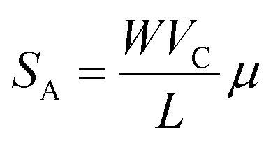
The magnetic responses of the GHEs were then measured on the Hall probe station. All the measurements were carried out at room temperature and ambient atmosphere, which is a huge advantage over traditional applications of SMMs. During the measurement, a constant voltage/current bias (VC/IC) was applied between the electrodes named drain and source. At the same time, an external magnetic field (B0) normal to the plane of sensors would generate a constant Hall voltage (VHall) between the electrodes VH1 and VH2 due to the Hall effect.24
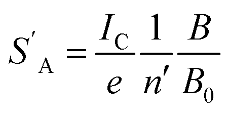
Sensitivity is a key parameter to benchmark the performance of Hall sensors. The Hall sensors with high sensitivity can detect magnetic field with high signal–noise ratio and thus reduce the cost of amplifications.23,32 The absolute sensitivity (SA) of GHEs is defined as the ratio of Hall voltage and external magnetic field,19,24
 | (1) |
We first consider Hall sensors powered by a constant voltage. The absolute sensitivity of pristine GHEs working at voltage mode is determined as follows,19,24
 | (2) |
| B = BMM + B0 | (3) |
 | (4) |
 | (5) |
It is evident that the sensitivity of graphene–SMMs hybrid Hall sensors is the compromise between the mobility decrease and magnetic field influence. The μ′ is decreased, but the S′A is increased. From the eqn (5), we can conclude that the S′A enhancement can be ascribed to the B/B0, and it may be because the magnetic center influence of SMMs affects the total magnetic field applied at Hall sensors (Fig. 2c). Fig. 2d demonstrates the linearity errors of GHEs before and after decorating molecular magnets. Both the pristine and SMMs modified GHEs exhibit excellent linearity with linearity error less than 1.5%. SMMs modifications avoid decreasing the sensing accuracy of Hall sensors. This is attributed to the linear relationship between BMM and B0 as shown in eqn (3). The voltage-related sensitivity, defined as SV = SA/V, is widely used as an important metric to benchmark the magnetic sensitivity of different Hall sensors excluding the impact of driving voltage. The voltage sensitivity has an average increase of 44.9% (from 0.069/T to 0.100/T) after SMMs modifications (Fig. 2e). It is worth mentioning that the SV of the SMMs–graphene hybrid Hall element outperforms silicon based Hall elements (SV = 0.07/T).21
We then conducted the magnetic detection experiment in current mode. The Hall sensors were powered by a constant current of 0.1 mA. Based on theoretical calculations, the absolute sensitivity of the Hall sensor in current mode is inversely proportional to the carrier concentration,19,24
 | (6) |
 | (7) |
 | ||
| Fig. 3 Comparison of magnetic responses between pristine and SMM-modified GHEs in current mode. (a) VH–B curves of pristine GHEs (blue line) and SMM modified GHEs (red line) under current of 0.1 mA. The dashed lines denote the linear fitting results of the VH–B curves. (b) The linearity errors of the pristine and SMM modified GHEs. (c) Sensitivity statistics of GHEs before and after the modification of SMMs. (d) Cycle test of the magnetic responses within six magnetic detection loop after modification of 10−7 mol L−1 molecular magnets in voltage (denoted by orange diamonds) and current (denoted by blue hexagons) modes. S0 represents the magnetic sensitivity of the GHEs during the first magnetic sensing cycle. | ||
Therefore, the absolute sensitivity can be described this way,
 | (8) |
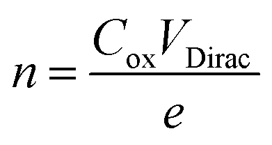
As for typical back-gate transistors, the carrier density of graphene is proportional to its Dirac point voltage,
 | (9) |
Based on eqn (8) and (9), we can get the relation between S′A and V′Dirac in current mode,
 | (10) |
As discussed in voltage mode, after modifying SMMs, the V′Dirac shifted positively, but S′A increase to 0.0959 V T−1. The enhancement may result from the magnetic center effect of SMMs and the magnetic molecules can affect graphene field environment because of the very close range interaction between graphene and SMMs at room temperature.13,33,34
After the modifications, the Hall sensors still shows tiny linearity error of less than 1.5% (Fig. 3b). The current sensitivity has an average increase of 59.0% (from 668 to 1062 V A−1 T−1) after SMMs modifications (Fig. 3c). To make a comparison, the SI of the SMMs–graphene hybrid Hall element outperforms silicon based Hall elements (SI = 100 V A−1 T−1) and commercialized III-V compounds Hall sensors (SI = 200 V A−1 T−1).24
Fig. 3d demonstrates the cycle test of the SMMs-modified GHEs within six magnetic detection loop in current (denoted by orange diamonds) and voltage (denoted by blue hexagons) modes. The floating range is less than 5%, indicating that the repeatability of our SMMs-modified GHEs is excellent.
Finally, we investigated the SMMs-concentration dependent magnetic detection performance of the GHEs. Fig. 4a shows the SMMs concentration dependent magnetic sensitivity of GHEs in current and voltage modes. It is clear that the sensitivity of GHEs increases when SMM concentration reaches 10−7 mol L−1 but declines when concentration exceeds 10−7 mol L−1. The sensitivities are even lower than those of the pristine GHEs at the concentration of 10−3 mol L−1. Based on the electronic measurements, graphene completely changes to p-type transport behavior when the concentration reaches 10−3 mol L−1 (Fig. S4†). The strong p-type carrier charge transfer is originated from the increasing residue dichloromethane with the additional modifications processes.26 At the same time, the mobility significantly declines to as low as 420 cm2 V−1 s−1. The additional scattering is due to the scatterings of clusters and crystallizations formed at high SMMs concentrations.26 Some clusters and crystallizations become visible under optical microscopes (see the ESI, Fig. S5†). As for Hall sensors, the offset voltage refers to the output Hall voltage when no magnetic field stimulation is applied. Generally, the offset voltage should be tuned as small as possible so as to reduce the cost of back-end calibrations. Fig. 4b shows the offset voltage as a function of the SMMs concentrations. In both the current and voltage modes, the offset voltages are within ±2 mV. These values are competitive compared with the silicon, III-V compounds and graphene Hall sensors.19,24 In addition, a sweeping direction test was carried out to further benchmark the reliability of our SMMs-modified GHEs. We selected a device decorated with 10−3 mol L−1 molecular magnets to conduct the experiment. Fig. 4c and d demonstrate the magnetic responses of GHEs with different sweep directions in voltage and current mode, respectively. These almost identical curves prove that our SMMs–graphene hybrid Hall sensors are independent with the external magnetic field sweeping directions. To sum up the magnetic response tests, graphene–SMMs hybrid structures enhance the sensitivity while maintain excellent linearity, offset voltage, repeatability and stability in magnetic sensing.
 | ||
| Fig. 4 Concentration dependent performance and magnetic sweeping direction test of SMM-modified GHEs. (a) SMM concentration dependent magnetic sensitivity of GHEs in current and voltage modes. (b) SMM concentration dependent offset voltages of GHEs in current and voltage modes. (c) VH–B curves of SMM-modified GHEs working at voltage mode and (d) current mode with opposite magnetic field sweeping direction. The concentration of SMM is 10−3 mol L−1. The blue dashed lines show the magnetic response with sweeping direction from south to north and the green solid lines show the magnetic response with sweeping direction from north to south. | ||
Conclusions
We report herein an easy way to apply the magnetic properties of SMMs at room temperature and enhance the sensitivity of GHEs by constructing a graphene–SMMs hybrid structure. The SMMs modification technique is directly applicable in situ onto GHEs without introducing complicated process. During the magnetic test, the sensitivity of the GHEs has an average increase of 44.9% in voltage mode and 59.0% in current mode. The sensitivity enhancement may result from the magnetic center introduction of SMMs at room temperature. The magnetic molecules may affect the graphene field environment leading to Hall signal change. Meanwhile, the Hall devices maintain other outstanding properties in magnetic detection, i.e. linearity (within ±1.5%), offset voltage (within ±2 mV), repeatability (sensitivity floating percentage within 5% during cycle tests) and stability (independent with magnetic field sweeping directions). Based on the graphene–SMMs hybrid structure, we are capable of utilizing the magnetic properties of SMMs at room temperature to enhance the sensitivity of magnetic detections.Acknowledgements
We are grateful for the financial support from the National Natural Science Foundation of China (61390502), the National Major State Basic Research Development Program (2013CB933403), and the Strategic Priority Research Program of the Chinese Academy of Sciences (XDB 12030100).Notes and references
- N. W. Daniel, E. P. W. Richard and A. L. Richard, Chem. Rev., 2013, 113, 5110 CrossRef PubMed.
- N. Domingo, E. Bellido and D. Ruiz-Molina, Chem. Soc. Rev., 2012, 41, 258 RSC.
- X. Y. Wang, A. Carolina and R. D. Kim, Chem. Soc. Rev., 2011, 40, 3213 RSC.
- L. Bogani and W. Wernsdorfer, Nat. Mater., 2008, 7, 179 CrossRef CAS PubMed.
- P. Dawid, H. I. Southerland, C. Avendaño, A. Prosvirin, C. Sanders, W. Wernsdorfer, K. S. Pedersen, J. Dreiser, R. Clérac, J. Nehrkorn, G. G. Simeoni, A. Schnegg, K. Holldack and K. R. Dunbar, J. Am. Chem. Soc., 2015, 137, 14406 CrossRef PubMed.
- M. N. Leuenberger and D. Loss, Nature, 2001, 410, 789 CrossRef CAS PubMed.
- J. Lehmann, A. Gaita-Arino, E. Coronado and D. Loss, J. Mater. Chem., 2009, 19, 1672 RSC.
- J.-P. Cleuziou, W. Wernsdorfer, V. Bouchiat, T. Ondarcuhu and M. Monthioux, Nat. Nanotechnol., 2006, 1, 53 CrossRef CAS PubMed.
- C. Cervetti, A. Rettori, M. G. Pini, A. Cornia, A. Repollés, F. Luis, M. Dressel, S. Rauschenbach, K. Kern, M. Burghard and L. Bogani, Nat. Mater., 2016, 15, 164 CrossRef CAS PubMed.
- M. Affronte, J. Mater. Chem., 2009, 19, 1731 RSC.
- K. Hong and W. Y. Kim, Angew. Chem., Int. Ed., 2013, 52, 3389 CrossRef CAS PubMed.
- K. Katoha, H. Isshiki, T. Komedab and M. Yamashita, Coord. Chem. Rev., 2011, 255, 2124 CrossRef.
- A. Candini, S. Klyatskaya, M. Ruben, W. Wernsdorfer and M. Affronte, Nano Lett., 2011, 11, 2634 CrossRef CAS PubMed.
- A. Giusti, G. Charron, S. Mazerat, J.-D. Compain, P. Mialane, A. Dolbecq, E. Riviere, W. Wernsdorfer, R. N. Biboum, B. Keita, L. Nadjo, A. Filoramo, J.-P. Bourgoin and T. Mallah, Angew. Chem., Int. Ed., 2009, 48, 4949 CrossRef CAS PubMed.
- L. Bogani, C. Danieli, E. Biavardi, N. Bendiab, A.-L. Barra, E. Dalcanale, W. Wernsdorfer and A. Cornia, Angew. Chem., Int. Ed., 2009, 48, 746 CrossRef CAS PubMed.
- J. F. Schenck, Med. Phys., 1996, 23, 815 CrossRef CAS PubMed.
- J. S. Miller, Chem. Soc. Rev., 2011, 40, 3266 RSC.
- S. Sasha, A. D. Dmitriy, H. B. D. Geoffrey, M. K. Kevin, J. Z. Eric, A. S. Eric, D. P. Richard, T. N. SonBinh and S. R. Rodney, Nature, 2006, 442, 282 CrossRef PubMed.
- H. Xu, L. Huang, Z. Zhang, B. Chen, H. Zhong and L.-M. Peng, Appl. Phys. Lett., 2013, 103, 112405 CrossRef.
- R. Shi, H. Xu, B. Chen, Z. Zhang and L.-M. Peng, Appl. Phys. Lett., 2013, 102, 113102 CrossRef.
- L. Huang, H. Xu, Z. Zhang, C. Chen, J. Jiang, X. Ma, B. Chen, Z. Li, H. Zhong and L.-M. Peng, Sci. Rep., 2014, 4, 5548 CAS.
- H. Xu, Z. Zhang, R. Shi, H. Liu, Z. Wang, S. Wang and L.-M. Peng, Sci. Rep., 2013, 3, 1207 Search PubMed.
- L. Huang, Z. Zhang, B. Chen, X. Ma, H. Zhong and L.-M. Peng, Appl. Phys. Lett., 2014, 104, 183106 CrossRef.
- R. S. Popovic, Hall Effect Devices, Institute of Physics Publishing, London, 2004 Search PubMed.
- S. Kyatskaya, J.-R. Galan-Mascaros, L. Bogani, F. Hennrich, M. Kappes, W. Wernsdorfer and M. Ruben, J. Am. Chem. Soc., 2009, 131, 15143 CrossRef CAS PubMed.
- M. Lopes, A. Candini, M. Urdampilleta, A. Reserbat-Plantey, V. Bellini, S. Klyatskaya, L. Marty, M. Ruben, M. Affronte, W. Wernsdorfer and N. Bendiab, ACS Nano, 2010, 4, 7531 CrossRef CAS PubMed.
- X. Ling, L. Xie, Y. Fang, H. Xu, H. Zhang, J. Kong, M. S. Dresselhaus, J. Zhang and Z. Liu, Nano Lett., 2010, 10, 553 CrossRef CAS PubMed.
- D. Geng, H. Wang, Y. Wan, Z. Xu, B. Luo, J. Xu and G. Yu, Adv. Mater., 2015, 27, 4195 CrossRef CAS PubMed.
- N. S. Sariciftci, A. J. Heeger, V. Krasevec, P. Venturini, D. Mihailovic, Y. Cao, J. Libert and J. L. Bredas, Synth. Met., 1994, 62, 107 CrossRef CAS.
- X. Dong, Y. Shi, Y. Zhao, D. Chen, J. Ye, Y. Yao, F. Gao, Z. Ni, T. Yu and Z. Shen, Phys. Rev. Lett., 2009, 102, 135501 CrossRef PubMed.
- S. Kim, J. Nah, I. Jo, D. Shahrjerdi, L. Colombo, Z. Yao, E. Tutuc and S. K. Banerjee, Appl. Phys. Lett., 2009, 94, 062107 CrossRef.
- B. Chen, L. Huang, X. Ma, L. Dong, Z. Zhang and L.-M. Peng, Carbon, 2015, 94, 585 CrossRef CAS.
- G. M. Gusev, C. A. Duarte, A. A. Quivy, T. E. Lamas and J. R. Leite, Phys. Rev. B: Condens. Matter Mater. Phys., 2005, 71, 165311 CrossRef.
- K. Tauber, A. Honemann, M. Gradhand and I. Mertig, Phys. Rev. B: Condens. Matter Mater. Phys., 2015, 91, 220404 CrossRef.
Footnotes |
| † Electronic supplementary information (ESI) available. See DOI: 10.1039/c6ra27673c |
| ‡ These authors contributed equally to the paper. |
| This journal is © The Royal Society of Chemistry 2017 |