
 Open Access Article
 This Open Access Article is licensed under a Creative Commons Attribution-Non Commercial 3.0 Unported Licence
Enhanced charge carrier transport in spray-cast organic solar cells using solution processed MoO3 micro arrays
Ran Jia,
Jiang Chengab,
Xin Yangab,
Junsheng Yu *a and
Lu Li*b
*a and
Lu Li*b
aState Key Laboratory of Electronic Thin Films and Integrated Devices, School of Optoelectronic Information, University of Electronic Science and Technology of China, Chengdu 610054, P. R. China
bCo-Innovation Center for Micro/Nano Optoelectronic Materials and Devices, Research Institute for New Materials and Technology, Chongqing University of Arts and Sciences, Chongqing 402160, P. R. China
First published on 13th January 2017
Abstract
A toward all spray fabrication routine was used to fabricate organic solar cells (OSCs), in which a molybdenum oxide (MoO3) micro array was directly deposited on the active layer, and the influence of the hole transporting property on the OSC performance was studied. The component and morphology of the MoO3 array as well as the effect on OSCs performance has been investigated. By using the solution processed MoO3, we obtained a 62.7% enhancement to 3.4% in PCE compared to the non-MoO3 device base on the P3HT system. Photovoltaic measurement and impedance analysis indicated that the MoO3 micro array has modified the interface between the electron donor and anode. By improving the ratio of the precursor solvent, the carrier transport performance was further improved. This approach significantly enhances our understanding of the application of MoO3 micro arrays in all-sprayed OSCs, and indicating that this simple method has good prospects for the handy commercial fabrication of OSCs.
1. Introduction
Solution-processable organic solar cells (OSCs) have attracted remarkable interest since they possess special merits such as lightweight, flexibility, large-scale manufacturing and low cost-effect.1–4 The spin coating method, with the advantage of reproducibility and easy operation, has been widely used for the fabrication of efficient OSCs with a high power conversion efficiency (PCE) of more than 11%.5 Unfortunately, conventional spin coating is difficult to be developed as an effective large-scale production method, since the thickness consistency of films can no longer be assured if the film area reaches a certain size. Furthermore, this popular technique has a low utilization rate of materials and is limited on smooth rigid substrates.6–8 In this case, several novel large-scale processes including inject printing, blade coating, and roll-to-roll processing have gained considerable attention.9–11 Spray coated deposition has been well reported for the fabrication of organic function films, especially active layers as well as polymer buffer layers, meeting the need of large-scale OSCs fabrication.12–14It is well known that the typical bulk heterojunction (BHJ) OSCs are fabricated with a transparent conductive cathode, a cathode buffer layer (CBL), an anode buffer layer (ABL) and an active layer sandwiched between the CBL and ABL.15,16 Researchers have expended extensive effort to prepare high quality active layer for efficient OSCs using a spray coated processing technique. In our previous work, a high PCE of 7.62% for the OSCs with a pneumatic spray coated PTB7:PC71BM was achieved.17 However, the study of spray coated buffer layer is very limited. Polymer buffer layers are more inclined to be chosen for the fabrication of all sprayed OSCs, because they are easily dissolved in organic solvents. However, polymer buffer layers usually have a low stability, resulting in an unsatisfactory lifetime. For example, the widely used ABL PEDOT:PSS is both hygroscopic and acidic, which has an associated reduction in device stability.18 Inorganic buffer layers are much more stable and suitable for high lifetime OSCs preparation. Unfortunately, it is much difficult to deposition inorganic buffer materials by solution method especially on active layer, since they usually need a high substrate temperature for annealing, even some of the raw materials could not be solubilized.
Recently, a solution process of ZnO CBL was processed at a comfortable low temperature (∼150 °C) by an ultrasonic spray pyrolysis using zinc–ammonia solution. And a PCE of 3.7% for the rigid P3HT:PCBM solar cells and a PCE of 2.8% for the flexible solar cells were reported.19 This low temperature solution process encouraged us to deposit inorganic ABLs on the organic active layer directly to develop a simple all-spray coating routine for preparing OSCs. As well known, the promising alternative ABLs are metal oxide with strong hole-transporting ability and stability such as molybdenum oxide (MoO3),20–23 vanadium oxide (V2O5),21,23 and nickel oxide (NiO).24,25 In particular, MoO3 is non-toxic and possesses deep-lying electronic states to be one of the most promising materials for the fabrication of high efficiency OSCs.5
In this study, our initial aim is to develop an ultrasonic spray coating method for low temperature deposition of MoO3 film. We chose the easily decomposed material ammonium heptamolybdate ((NH4)6Mo7O24·4H2O) as the precursor solution. However, we found that MoO3 is not apt to form continuous film on all substrates that we have tried including P3HT:PCBM blend film. Microscope shows that P3HT:PCBM was discrete MoO3 micro arrays. Nevertheless, we found that the micro arrays have the similar function of improving the interfacial contact as MoO3 thin film, and a 62.7% enhancement to 3.4% in PCE compared to non-MoO3 P3HT:PCBM solar cells was obtained. In particular, most parts of OSCs except the silver anode are fabricated by spray-coating method under atmospheric condition, which was one step closer to the realization of low-cost, high lifetime and large-scale OSCs.
2. Experimental
2.1 Fabrication section
The configuration of photovoltaic device is ITO/ZnO (40 nm)/P3HT:PC61BM (300 nm)/MoO3 array/Ag (100 nm), as shown in Fig. 1(a). Patterned ITO-coated glass substrates with a sheet resistance of 10 Ω sq.−1 were consecutively cleaned in ultrasonic bath containing detergent, acetone, deionized water and ethanol for 10 min each step, then dried by nitrogen blow. A 50 nm ZnO layer was then grown on ITO film by ultrasonic spray pyrolysis at 150 °C as we depicted in our published works.19,26 Then, a 300 nm active layer of P3HT:PC61BM was cast from a solution with P3HT (99.9%, Aldrich) and (6,6)-phenyl-PCBM (99.9%, Lumtec) at ratio of 1![[thin space (1/6-em)]](https://www.rsc.org/images/entities/char_2009.gif) :0.9 wt% in 1,2-dichlorobenzene (DCB) at a concentration of 5 mg ml−1. The spray rate of P3HT:PC61BM solution was 0.075 ml min−1 and the N2 carrier gas flow rate was held at a rate of 18 L min−1. MoO3 was deposited on P3HT:PCBM blend film by ultrasonic spray pyrolysis at 80 °C using N2 as carrier gas at a flow rate of 10 L min−1, solution atomization rate was approximately 3 ml min−1. The spray apparatus was consisted of an ultrasonic transducer, an atomization chamber, an automatic X–Y table, a heating block and pipe fittings, as shown in Fig. 1(b). The ultrasonic transducer continuously converts solution into mist, which could be transport by carrier gas and then deposited on the surface of substrate. MoO3 precursor were carried out by dissolving ammonium heptamolybdate ((NH4)6Mo7O24·4H2O) in deionized water mixed with one or several organic solvents (methanol, isopropanol) with a desired concentration (0.2 wt%).
:0.9 wt% in 1,2-dichlorobenzene (DCB) at a concentration of 5 mg ml−1. The spray rate of P3HT:PC61BM solution was 0.075 ml min−1 and the N2 carrier gas flow rate was held at a rate of 18 L min−1. MoO3 was deposited on P3HT:PCBM blend film by ultrasonic spray pyrolysis at 80 °C using N2 as carrier gas at a flow rate of 10 L min−1, solution atomization rate was approximately 3 ml min−1. The spray apparatus was consisted of an ultrasonic transducer, an atomization chamber, an automatic X–Y table, a heating block and pipe fittings, as shown in Fig. 1(b). The ultrasonic transducer continuously converts solution into mist, which could be transport by carrier gas and then deposited on the surface of substrate. MoO3 precursor were carried out by dissolving ammonium heptamolybdate ((NH4)6Mo7O24·4H2O) in deionized water mixed with one or several organic solvents (methanol, isopropanol) with a desired concentration (0.2 wt%).
 | ||
| Fig. 1 (a) Device structure of the inverted OSC and (b) ultrasonic spray deposition system. | ||
2.2 Measurement method
The composition and electron structure of the MoO3 micro array was characterized by using X-ray photoelectron spectroscopy (XPS, Thermo ESCALAB). Surface morphology of the MoO3 micro array was characterized by three-dimensional microscope (DSX500, Olympus) and scanning electronic microscope (SEM, S4800 Hitachi). Current density–voltage (J–V) curves were measured using Keithley 2400 under a xenon lamp solar simulator (7IS0503A, Beijing SOFN) with an illumination power of 100 mW cm−2.4 All the measurements were carried out at ambient circumstance without encapsulation.3. Results and discussion
3.1 MoO3 spraying process
To accomplish a good uniformity for the films, the sprinkler is passed over the hot plate which was driven by the drive X–Y table. The sprinkler performed an S-shaped curve relative motive with the substrate. The precursor was atomized, transported and the decomposed to MoO3, NH3 and H2O, among which NH3 is gaseous, and MoO3 is expected to be the only solute in the solution.27,28 After the deposition process, the wafers were sequentially annealed in situ for 2 min to form a stable structure for MoO3.3.2 Component analysis by XPS
The surface characteristics of the MoO3 on silicon wafer were characterized by XPS. Before testing, MoO3 were etched using argon plasma for approximately 10 nm. The full scan spectrums of solution processed MoO3 with thermal evaporated MoO3 were shown in Fig. 2(a and b). O 1s and Mo 3d peaks of the two samples are shown in Fig. 2(c, d) and (e, f), respectively. The two full scan spectra are difficult to distinguish. Two main XPS resolved peaks belong to the typical doublet of Mo6+ at 232.2 eV and 235.5 eV are easy to be observed.5 By a more detailed analysis, the O 1s XPS spectrum exhibits asymmetric line shapes (Fig. 2(e and f)). The peak with lower binding (529.8 to 530.1) energy corresponds to O atoms in a MoO3 matrix. The second peak, at 530.5 to 531.0 eV is probably due to oxide impurities accumulated.29 The relative magnitude of the high-binding-energy O atoms was 35% in thermal enveloped MoO3 and 24% in solution processed MoO3, indicating the solution processed MoO3 has a more perfect composition than thermal evaporated. Mo5+ doublet at 233.4 and 230.7 of thermal evaporated MoO3 can also be detected by peak fitting analysis. The relative magnitude of Mo5+/Mo6+ is approximately 10%. On the contrary, the high resolution XPS spectrum of solution processed MoO3 reveals only Mo6+ oxidation state. It means that solution processed MoO3 films have less oxygen vacancies. The saturated valence state of Mo indicated that it is stable. The solution processed MoO3 might have a better performance in hole transporting than thermal evaporated sample, due to the less oxide impurities and stable Mo valence state. Thus, as an ABL material, the solution processed MoO3 is less sensitive to thickness than the evaporated MoO3. | ||
| Fig. 2 XPS spectra of different process MoO3 films. (a), (c) and (e) Full scan, Mo 3d core levels, O 1s core levels, deposited by vacuum thermal evaporation, respectively. (b), (d) and (f) Full scan, Mo 3d core levels, O 1s core levels, spray-coated in air, respectively. | ||
3.3 Deionized water as precursor solution
Initially, a very interesting phenomenon in our prepared MoO3 on P3HT:PCBM blend films was observed when the deionized water was the only solvent of precursor. MoO3 tended to form micro arrays instead of uniform films on the surface of active layer as well as the other substrates we have tried. As we seen in Fig. 3, the microscope image shows the spray-casted MoO3 micro array was consisted of a series of island of varying sizes. The size of islands shifted to larger when the spray time increased. Surprisingly, the density of micro islands is almost constant at approximately 1.8 × 103 mm−2. In conclusion, the MoO3 deposited by water solution of (NH4)6Mo7O24·4H2O is apt to gather into islands and aligning to grid.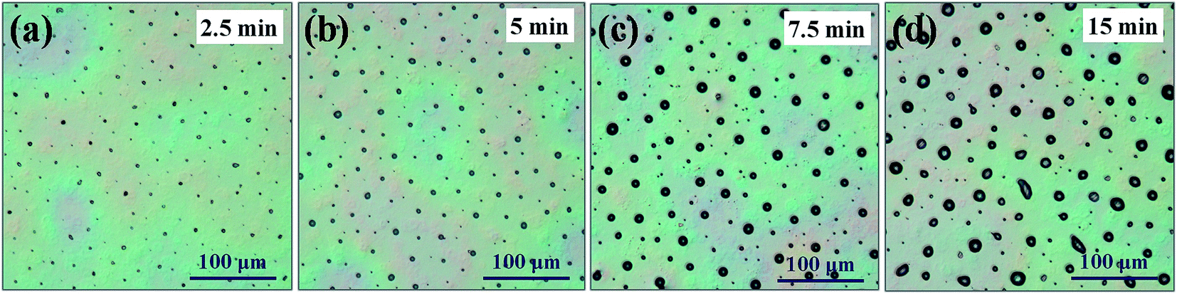 | ||
| Fig. 3 Microscope images of MoO3 array with water solvent in different spray time. (a) 2.5 min (b) 5 min (c) 7.5 min (d) 15 min (one cycle of X–Y table running time is 2.5 min). | ||
3.4 Multicomponent solvent system (MSS)
As the deionized water has a low vapor pressure and cannot volatilize from droplet timely, we conducted a systematic study of a multicomponent solvent system consisted of deionized water (DW), methanol (ME) and isopropanol (IPA) as the solvent of MoO3 precursor solution. The effect of MSS on the performance of spray coated OSCs was investigated. We prepared 4 samples in parallel, each sample having 4 cells with an active area of 0.07 cm2. The device performances are summarized in Table 1 and Fig. 4.| VOC (mV) | JSC (mA cm−2) | FF (%) | PCE (%) | |
|---|---|---|---|---|
| Thermal evaporated 5 nm MoO3 | 590 | 9.07 | 60.2 | 3.23 |
| Thermal evaporated 30 nm MoO3 | 577 | 7.52 | 54.3 | 2.36 |
| Non-MoO3 | 530 | 8.97 | 43.8 | 2.09 |
| DW | 603 | 8.35 | 56.0 | 2.82 |
|
||||
| Solvent (vol%) | ||||
IPA![[thin space (1/6-em)]](https://www.rsc.org/images/entities/i_char_2009.gif) :DW :DW |
||||
| 20:80 |
595 | 9.03 | 56.2 | 3.03 |
| 40:60 |
598 | 9.36 | 58.8 | 3.25 |
| 60:40 |
593 | 8.07 | 45.6 | 2.19 |
| 80:20 |
600 | 6.77 | 31.0 | 1.26 |
| ME:DW |
||||
| 20:80 |
596 | 8.82 | 57.8 | 3.03 |
| 40:60 |
596 | 8.33 | 56.2 | 2.79 |
| 60:40 |
597 | 7.95 | 44.0 | 2.09 |
| 80:20 |
604 | 7.03 | 25.5 | 1.08 |
| IPA:ME:DW |
||||
| 10:30:60 |
599 | 9.42 | 55.9 | 3.16 |
| 20:20:60 |
600 | 9.51 | 59.1 | 3.37 |
| 30:10:60 |
598 | 9.61 | 59.2 | 3.40 |
 | ||
| Fig. 4 (a), (b) and (c) J–V characteristics of OSCs with different MSSs; (d) EQE characteristics of OSCs based on MoO3 micro array in different MSSs. | ||
For the device without MoO3 ABL, the PCE was only 2.09% with an open circuit voltage (VOC) of 530 mV, a short circuit current density (JSC) of 8.97 mA cm−2, and a fill factor (FF) of 43.8%. The low performance was caused by the poor contact between active layer and Ag.30 When the solution processed MoO3 ABLs was employed, the devices showed a consistent improvement on VOC and FF, resulting in a higher PCE. When using DW at the solvent of precursor, the OSCs yielded an improved PCE of 2.82%. For the IPA:DW MSS, the device showed a gradually rise in performance when IPA ratio increase from 0 to 40 vol%. Especially, the optimized IPA:DW MSS with a ratio of 40:60 vol% presents 12% enhanced JSC from 8.35 to 9.36 mA cm−2, and 15% enhanced PCE from 2.82% to 3.25%. When the IPA volume content ratio exceeds 40 to 80 vol%, JSC and PCE gradually decreased to 6.77 mA cm−2 and 1.26%. For the ME:DW MSS, similar to the case of IPA:DW MSS, the highest device performance was obtained where the PCE was 3.03% with VOC of 596 mV, JSC of 8.82 mA cm−2, and FF of 57.8%. Compared with the solution processed MoO3, the device with 5 nm thermal evaporated MoO3 shows a lower VOC of 590 mV, JSC of 9.07 mA cm−2 and the highest FF of 60.2%. The device with 30 nm thermal evaporated MoO3 shows a lowest PCE of 2.36% with VOC of 577 mV, JSC of 7.52 mA cm−2, and FF of 54.3%. The device performance with thermal evaporated MoO3 is sensitive to the thickness of the ABL.
The performance of OSCs increased with the enhancement of ME or IPA volume in the binary solvent system. However, both of them exhibit a gradual degradation instead of steady improvement in device performance when the content reached more than 40%. It seems that the water vapor is not the essential effect on the active layer. The surface morphology of MoO3 reveals the nature of the MSS effect on the device, as shown in Fig. 5. When using DW in the solvent of precursor, MoO3 has a less effective contact area with the active layer and the island was nearly spherical. However, when the precursor contained a part of IPA or ME, the MoO3 arrays were composed of flat islands as shown in Fig. 5(b). The roughness of interface decreases obviously. And from the performance respects, the result suggests that the flat MoO3 array can enhance the hole collection at the interface between the ITO and active layer.31 Due to the JSC and FF increased obviously, which resulted in a high PCE. Combining with the broader area of MoO3 islands, we speculate that the charge-carrier transport channel between the active layer and the anode became much broader. The accurate conclusion will be verified in the subsequent experiments.
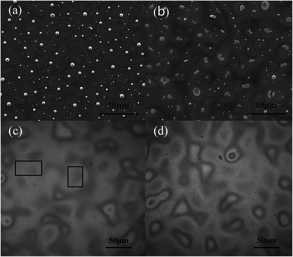 | ||
| Fig. 5 SEM images of MoO3 micro array with different MSS of (a) DW; (b) DW:IPA:ME (60:30:10 vol%). Metallographic microscope images of active layer with different MSS of (c) IPA:DW (80:20 vol%); (d) ME:DW (80:20 vol%). | ||
It is well known that both of IPA and ME are frequently used polar organic solvent, which have been investigated to treat active layer.32,33 It is also a reason of performance improved by introducing IPA and ME. However, the increasing content of IPA or ME caused a destruction of the P3HT:PCBM under the condition of annealing. When the concentration reached to a certain amount, it destroyed the morphology of active layer and caused many voids or pinholes as shown in Fig. 5(c and d), leading to a low device performance.
To further improve the performance of OSCs while increasing the repeatability with solution processed MoO3 arrays, a ternary solvent system was introduced. Keeping a proper atomization efficiency makes not only the measurement of mist suitable but also the rate of mist generation uniform. We observed that the atomization efficiency of solvents is dependent on solvent viscosity. A high viscosity causes the low atomization efficiency. The viscosities of IPA, ME and DW are 24.0 mPa s, 0.6 mPa s and 1.0 mPa s, respectively. Consequently, we have adjusted the ratio of DW, ME and IPA. The efficient device performance was obtained when DW ratio is 60% and IPA:ME is 1:1 to 3:1. The best PCE is 3.40% when IPA:ME:DW is 3:1:6.
Fig. 6(a and b) show the morphology of 5 nm and 30 nm thermal evaporated MoO3. It can be seen that, when the thickness of MoO3 is 5 nm, the film is discontinuous, which is similar to the spray-casted one with DW precursor solution. When the thickness reaches 30 nm, the film is quite flat and continuous. Based on device performance, this continuous film causes a lower performance compared with the MoO3 micro arrays via the poor conductivity.
 | ||
| Fig. 6 SEM images of thermal evaporated MoO3 with different thickness of (a) 5 nm; (b) 30 nm. | ||
Fig. 4(d) shows the results of external quantum efficiency (EQE) measurement for OSCs fabricated by using different solvent systems. The spectrum of the device with IPA:ME:DW solvent system shows a higher EQE than others and a maximum of 63.9% at a wavelength of 520 nm. The relatively high EQE maybe come from an improvement of the interface contact between donor and anode. This result indicated that the solution processed MoO3 by using the MSS could lead to the improved charge transfer efficiency.
3.5 Equivalent circuit model and impedance analysis
To investigate the carrier dynamics, Nyquist plots were analyzed using an equivalent circuit as shown in Fig. 7. The calculated parameters are also shown in Table 2. We can see that the calculated plots are in good accordance with a simulated curve. The parallel circuit of R1 and CPE1 represent the D/A interface, R2 and C2 represent the interface of active layer and electrodes, R3 represents the resistance of electrodes. R1 and CPE1 related to active layer for different devices are approximately identical. Real impedances Z′ of OPVs decrease significantly when the MSS was contain a certain amount of IPA and ME, resulting in the high JSC for the OSCs.34 A high R2 of device with DW suggests that the interface between the active layer and the buffer layer is not efficient for charge transport. For devices with IPA:ME:DW in a proportion of 30:10:60, R2 decreased to the minimum at 1.01 × 10⁶ Ω cm2,35 revealing that the interfacial resistance between the active layer and the solution processed MoO3 is minimized.
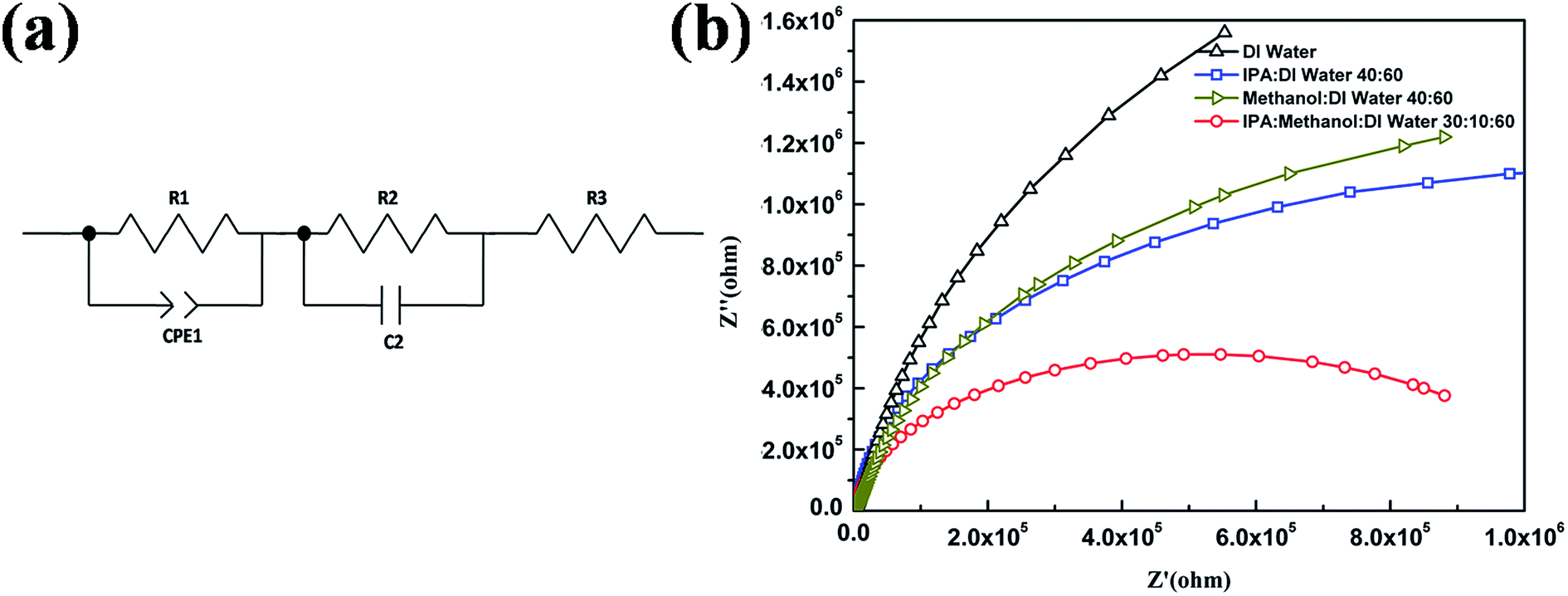 | ||
| Fig. 7 (a) Equivalent circuit model of the devices. (R1 and CPE1, R2 and C2, R3 represent equivalent of D/A interface, interface between active layer and electrodes, resistance of electrodes, respectively). (b) Cole–Cole plots of the devices with different MSS. | ||
| Device | R1 (Ω) | CPE1-T (F cm−2) | CPE1-P | R2 (Ω) | C2 (F) |
|---|---|---|---|---|---|
| DW | 2.45 × 10³ | 1.07 × 10⁻⁹ | 0.96 | 4.04 × 10⁶ | 1.85 × 10⁻⁹ |
| IPA:DW 40:60 |
2.52 × 10³ | 2.59 × 10⁻⁹ | 0.95 | 2.08 × 10⁶ | 1.67 × 10⁻⁹ |
| ME:DW 40:60 |
2.65 × 10³ | 1.19 × 10⁻⁹ | 0.95 | 2.29 × 10⁶ | 1.74 × 10⁻⁹ |
| IPA:ME:DW 30:10:60 |
2.57 × 10³ | 2.68 × 10⁻⁹ | 0.95 | 1.01 × 10⁶ | 1.42 × 10⁻⁹ |
4. Conclusions
Solution processed MoO3 micro arrays were successfully grown on the OSC active layers by using ultrasonic spray coating method at a very low temperature of 80 °C. The charge carrier transport between the active layer and the anode was improved with the solution processed MoO3 micro arrays. Thus, the JSC and FF obviously increased, and a higher PCE was obtained. The carrier transport performance was further improved by the introduction of the MSS for MoO3 precursor. When DW ratio is 60% and IPA:ME is 1:1 to 3:1, the OSCs with solution processed MoO3 showed a highest PCE of 3.40%. This technique is straight-forward, low cost, meeting the requirement of roll-to-roll process and compatible with large scale and high lifetime organic photoelectric devices.
Acknowledgements
The authors gratefully acknowledge the financial support from National Natural Science Foundation of China (NSFC) (Grant Nos. 61675041, 51503022 and 61505018); the Foundation for Innovation Research Groups of the NSFC (Grant No. 61421002); Science & Technology Department of Sichuan Province via Grant No. 2016HH0027; Technology Project from Chongqing Education Committee (Grant No. KJ1401113); Chongqing Science & Technology Commission (Grant No. cstc2013jcyjys50001); Chongqing University of Arts and Science (Grant No. R2012CJ18 & Z2013CJ02).References
- Q. An, F. Zhang, J. Zhang, W. Tang, Z. Deng and B. Hu, Energy Environ. Sci., 2015, 9, 281–322 Search PubMed
.
- Q. An, F. Zhang, L. Li, J. Wang, Q. Sun, J. Zhang, W. Tang and Z. Deng, ACS Appl. Mater. Interfaces, 2015, 7, 3691–3698 CAS
- M. Zhang, F. Zhang, Q. An, Q. Sun, W. Wang, J. Zhang and W. Tang, Nano Energy, 2016, 22, 241–254 CrossRef CAS
- Q. An, F. Zhang, L. Li, J. Wang, J. Zhang, L. Zhou and W. Tang, ACS Appl. Mater. Interfaces, 2014, 6, 6537–6544 CAS
- C. Xu, P. Cai, X. Zhang, Z. Zhang, X. Xue, J. Xiong and J. Zhang, Sol. Energy Mater. Sol. Cells, 2017, 159, 136–142 CrossRef CAS
- Y. Liu, X. Wan, F. Wang, J. Zhou, G. Long, J. Tian, J. You, Y. Yang and Y. Chen, Adv. Energy Mater., 2011, 1, 771–775 CrossRef CAS
- C. J. Brabec and J. R. Durrant, MRS Bull., 2008, 33, 670–675 CrossRef CAS
- T. Wang, N. W. Scarratt, H. Yi, A. D. F. Dunbar, A. J. Pearson, D. C. Watters, T. S. Glen, A. C. Brook, J. Kingsley and A. R. Buckley, Adv. Energy Mater., 2013, 3, 505–512 CrossRef CAS
- F. C. Krebs, M. Jørgensen, K. Norrman, O. Hagemann, J. Alstrup, T. D. Nielsen, J. Fyenbo, K. Larsen and J. Kristensen, Sol. Energy Mater. Sol. Cells, 2009, 93, 422–441 CrossRef CAS
- C. N. Hoth, S. A. Choulis, P. Schilinsky and C. J. Brabec, Adv. Mater., 2007, 19, 3973–3978 CrossRef CAS
- T. Aernouts, T. Aleksandrov, C. Girotto, J. Genoe and J. Poortmans, Appl. Phys. Lett., 2008, 92, 33306 CrossRef
- G. Susanna, L. Salamandra, T. M. Brown, A. D. Carlo, F. Brunetti and A. Reale, Sol. Energy Mater. Sol. Cells, 2011, 95, 1775–1778 CrossRef CAS
- D. Vak, S. S. Kim, J. Jo, S. H. Oh, S. I. Na, J. Kim and D. Y. Kim, Appl. Phys. Lett., 2007, 91, 81102 CrossRef
- W. Ma, C. Yang, X. Gong, K. Lee and A. J. Heeger, Adv. Funct. Mater., 2005, 15, 1617–1622 CrossRef CAS
- Z. He, C. Zhong, S. Su, M. Xu, H. Wu and Y. Cao, Nat. Photonics, 2012, 6, 593–597 CrossRef CAS
- L. Chen, P. Wang, F. Li, S. Yu and Y. Chen, Sol. Energy Mater. Sol. Cells, 2012, 102, 66–70 CrossRef CAS
- D. Zheng, J. Huang, Y. Zheng and J. Yu, Org. Electron., 2015, 25, 275–282 CrossRef CAS
- G. Li, C. W. Chu, V. Shrotriya, J. Huang and Y. Yang, Appl. Phys. Lett., 2006, 88, 253503–253505 CrossRef
- J. Cheng, Q. Wang, C. Zhang, X. Yang, R. Hu, J. Huang, J. Yu and L. Li, J. Mater. Sci.: Mater. Electron., 2016, 27, 7004–7009 CrossRef CAS
- D. Y. Kim, J. Subbiah, G. Sarasqueta, F. So, H. Ding, Irfan and Y. Gao, Appl. Phys. Lett., 2009, 95, 93304 CrossRef
- Irfan, H. Ding, Y. Gao and D. Y. Kim, Appl. Phys. Lett., 2010, 96, 73304 CrossRef
- V. Shrotriya, G. Li, Y. Yao and C. W. Chu, Appl. Phys. Lett., 2006, 88, 73508 CrossRef
- G. Li, C. W. Chu, V. Shrotriya, J. Huang and Y. Yang, Appl. Phys. Lett., 2006, 88, 253503–253505 CrossRef
- J. R. Koo, S. J. Lee, H. W. Lee, D. H. Lee, H. J. Yang, W. Y. Kim and Y. K. Kim, Opt. Express, 2013, 21, 11086–11094 CrossRef CAS PubMed
- K. X. Steirer, P. F. Ndione, N. E. Widjonarko, M. T. Lloyd, J. Meyer, E. L. Ratcliff, A. Kahn, N. R. Armstrong, C. J. Curtis and D. S. Ginley, Adv. Energy Mater., 2011, 1, 813–820 CrossRef CAS
- J. Cheng, R. Hu, Q. Wang, C. Zhang, Z. Xie, Z. Long, X. Yang and L. Li, Int. J. Photoenergy, 2015, 2015, 1–8 CrossRef
- D. Parviz, M. Kazemeini, A. M. Rashidi and K. J. Jozani, J. Nanopart. Res., 2009, 12, 1509–1521 CrossRef
- S. Murase and Y. Yang, Adv. Mater., 2012, 24, 2459–2462 CrossRef CAS PubMed
- C. Wang, I. Irfan, X. Liu and Y. Gao, J. Vac. Sci. Technol., B: Nanotechnol. Microelectron.: Mater., Process., Meas., Phenom., 2014, 32, 40801 Search PubMed
- N. Wang, J. Yu, Y. Zheng, Z. Guan and Y. Jiang, J. Phys. Chem. C, 2012, 116, 5887–5891 CAS
- S. Murase and Y. Yang, Adv. Mater., 2012, 24, 2459–2462 CrossRef CAS PubMed
- H. Zhou, Y. Zhang, J. Seifter, S. D. Collins, C. Luo, G. C. Bazan, T. Nguyen and A. J. Heeger, Adv. Mater., 2013, 25, 1646–1652 CrossRef CAS PubMed
- Y. Zheng, S. Li, D. Zheng and J. Yu, Org. Electron., 2014, 15, 2647–2653 CrossRef CAS
- E. P. Yao, C. C. Chen, J. Gao, Y. Liu, Q. Chen, M. Cai, W. C. Hsu, Z. Hong, G. Li and Y. Yang, Sol. Energy Mater. Sol. Cells, 2014, 130, 20–26 CrossRef CAS
- Y. Zheng, T. Goh, P. Fan, W. Shi, J. Yu and A. D. Taylor, ACS Appl. Mater. Interfaces, 2016, 8, 15724–15731 CAS
| This journal is © The Royal Society of Chemistry 2017 |